

Page 1
Thermocouple Conditioner and
a
FEATURES
Low Cost
Operates with Type J (AD596) or Type K (AD597)
Thermocouples
Built-In Ice Point Compensation
Temperature Proportional Operation – 10 mV/8C
Temperature Setpoint Operation – ON/OFF
Programmable Switching Hysteresis
High Impedance Differential Input
GENERAL DESCRIPTION
The AD596/AD597 is a monolithic temperature setpoint controller that has been optimized for use at elevated temperatures
such as those found in oven control applications. The device
cold junction compensates and amplifies a type J or K thermocouple input to derive an internal signal proportional to temperature. The internal signal is then compared with an externally
applied setpoint voltage to yield a low impedance switched output
voltage. Dead-Band or switching hysteresis can be programmed
using a single external resistor. Alternately, the AD596/AD597 can
be configured to provide a voltage output (10 mV/°C) directly from
a type J or K thermocouple signal. It can also be used as a standalone voltage output temperature sensor.
The AD596/AD597 can be powered with a single supply from
+5 V to +30 V, or dual supplies up to a total span of 36 V.
Typical quiescent supply current is 160 µA, which minimizes
self-heating errors.
The AD596/AD597 H package option includes a thermocouple
failure alarm that indicates an open thermocouple lead when
operated in the temperature proportional measurement mode.
The alarm output has a flexible format which can be used to
drive relays, LEDs or TTL logic.
The device is packaged in a reliability qualified, cost effective
10-pin metal can or SOIC and is trimmed to operate over an
ambient temperature range from +25°C to +100°C. Operation
over an extended ambient temperature range is possible with
slightly reduced accuracy. The AD596 will amplify thermocouple signals covering the entire –200°C to +760°C temperature range recommended for type J thermocouples while the
AD597 can accommodate –200°C to +1250°C type K inputs.
The AD596/AD597 has a calibration accuracy of ±4°C at an
ambient temperature of 60°C and an ambient temperature
stability specification of 0.05°C/°C from +25°C to +100°C. If
higher accuracy, or a lower ambient operating temperature is
required, either the AD594 (J thermocouple) or AD595 (K
thermocouple) should be considered.
*Protected by U.S. Patent No. 4,029,974.
Setpoint Controller
AD596*/AD597*
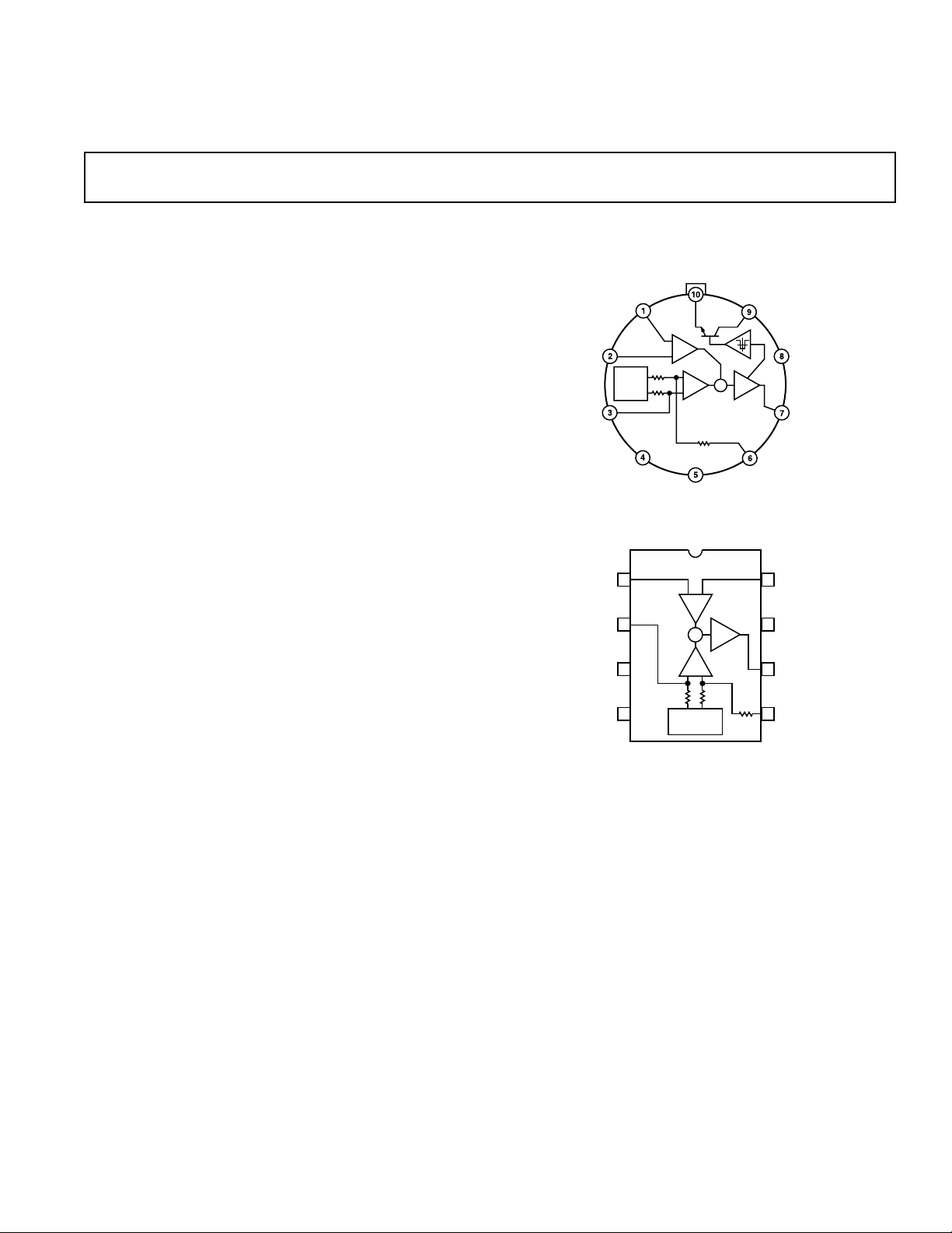
FUNCTIONAL BLOCK DIAGRAM
TO-100
–ALM
+
AD596/
AD597
–
+
A
–
+ALM
V+
A
+
V
OUT
FB
–IN
8
V+
7
V
6
OUT
FB
–IN
–
+IN
HYS
ICE
POINT
COMP
GND
G
+
–
G
+
V–
SOIC
AD597
+IN
1
+
G
HYS
2
GND
3
V–
45
+
G
+
ICE POINT
COMP
TOP VIEW
(Not to Scale)
PRODUCT HIGHLIGHTS
1. The AD596/AD597 provides cold junction compensation
and a high gain amplifier which can be used as a setpoint
comparator.
2. The input stage of the AD596/AD597 is a high quality instrumentation amplifier that allows the thermocouple to float
over most of the supply voltage range.
3. Linearization not required for thermocouple temperatures
close to 175°C (+100°C to +540°C for AD596).
4. Cold junction compensation is optimized for ambient temperatures ranging from +25°C to +100°C.
5. In the stand-alone mode, the AD596/AD597 produces an
output voltage that indicates its own temperature.
REV. B
Information furnished by Analog Devices is believed to be accurate and
reliable. However, no responsibility is assumed by Analog Devices for its
use, nor for any infringements of patents or other rights of third parties
which may result from its use. No license is granted by implication or
otherwise under any patent or patent rights of Analog Devices.
One Technology Way, P.O. Box 9106, Norwood, MA 02062-9106, U.S.A.
Tel: 781/329-4700 World Wide Web Site: http://www.analog.com
Fax: 781/326-8703 © Analog Devices, Inc., 1998
Page 2

AD596/AD597–SPECIFICA TIONS
(@ +608C and VS = 10 V, Type J (AD596), Type K (AD597) Thermocouple,
unless otherwise noted)
Model AD596AH AD597AH AD597AR
Min Typ Max Min Typ Max Min Typ Max Units
ABSOLUTE MAXIMUM RATINGS
+VS to –V
Common-Mode Input Voltage (–VS – 0.15) +V
Differential Input Voltage –V
Alarm Voltages
Operating Temperature Range –55 +125 –55 +125 –40 +125 °C
S
+ALM –V
–ALM –V
S
S
S
36 36 36 Volts
+V
S
S
(–VS – 0.15) +V
–V
(–VS +36) –V
+V
S
–V
S
S
S
S
+V
S
(–VS +36) –V
+V
S
(–VS – 0.15) +V
–V
–V
S
S
S
+V
(–VS +36) Volts
+V
S
S
S
Volts
Volts
Volts
Output Short Circuit to Common Indefinite Indefinite Indefinite
TEMPERATURE MEASUREMENT
(Specified Temperature Range
+25°C to +100°C)
Calibration Error
Stability vs. Temperature
1
2
–4 +4 –4 +4 –4 +4 °C
± 0.02 ± 0.05 ± 0.02 ± 0.05 ± 0.02 ± 0.05 °C/°C
Gain Error –1.5 +1.5 –1.5 +1.5 –1.5 +1.5 %
Nominal Transfer Function 10 10 10 mV/°C
AMPLIFIER CHARACTERISTICS
Closed Loop Gain
3
180.6 245.5 245.5 V/V
Input Offset Voltage °C × 53.21 + 235 °C × 41.27 – 37 °C × 41.27 – 37 µV
Input Bias Current 0.1 0.1 0.1 µA
Differential Input Range –10 +50 –10 +50 –10 +50 mV
Common-Mode Range (–VS – 0.15) (+VS – 4) (+VS – 0.15) (+VS – 4) (–VS – 0.15) (+VS – 4) Volts
Common-Mode Sensitivity–RTO 10 10 10 mV/V
Power Supply Sensitivity–RTO 1 10 1 10 1 10 mV/V
Output Voltage Range
Dual Supplies (–VS + 2.5) (+VS – 2) (–VS + 2.5) (+VS – 2) (–VS + 2.5) (+VS – 2) Volts
Single Supply 0 (+VS – 2) 0 (+VS – 2) 0 (+VS – 2) Volts
Usable Output Current
4
± 5 ± 5 ± 5mA
3 dB Bandwidth 15 15 15 kHz
ALARM CHARACTERISTICS
V
at 2 mA 0.3 0.3 Volts
CE(SAT)
Leakage Current 61 61 µA
5
Alarm Function Not Pinned Out
Operating Voltage at – ALM (+VS – 4) (+VS – 4) Volts
Short Circuit Current 20 20 mA
POWER REQUIREMENTS
Operating (+VS to –VS) ≤ 30 (+VS to –VS) ≤ 30 (+VS to –VS) ≤ 30 Volts
Quiescent Current
+V
S
–V
S
NOTES
1
This is a measure of the deviation from ideal with a measuring thermocouple junction of 175°C and a chip temperature of 60°C. The ideal transfer function is given by:
AD596: V
AD597: V
where V
error over the ambient temperature range of 25°C to 100°C with a thermocouple temperature of approximately 175°C.
2
Defined as the slope of the line connecting the AD596/AD597 CJC errors measured at 25°C and 100°C ambient temperature.
3
Pin 6 shorted to Pin 7.
4
Current Sink Capability in single supply configuration is limited to current drawn to ground through a 50 kΩ resistor at output voltages below 2.5 V.
5
Alarm function available on H package option only.
Specifications subject to change without notice.
Specifications shown in boldface are tested on all production units at final electrical test. Results from those tests are used to calculate outgoing quality levels. All min and max
specifications are guaranteed, although only those shown in boldface
= 180.57 × (Vm – Va + (ambient in °C) × 53.21 µV/°C + 235 µV)
OUT
= 245.46 × (Vm – Va + (ambient in °C) × 41.27 µV/°C – 37 µV)
OUT
, and Va represent the measuring and ambient temperatures and are taken from the appropriate J or K thermocouple table. The ideal transfer function minimizes the
m
160 300 160 300 160 300 µA
100 200 100 200 100 200 µA
are tested on all production units.
ORDERING GUIDE
Model Package Description Package Options
AD596AH TO-100 H-10A
AD597AH TO-100 H-10A
AD597AR* Plastic SOIC SO-8
*Consult factory for availability.
–2–
REV. B
Page 3
Table I. Output Voltage vs. Thermocouple Temperature (Ambient +608C, VS = –5 V, +15 V)
Thermocouple Type J AD596 Type K AD597
Temperature Voltage Output Voltage Output
8C mVmVmVmV
–200 –7.890 –1370 –5.891 –1446
–180 –7.402 –1282 –5.550 –1362
–160 –6.821 –1177 –5.141 –1262
–140 –6.159 –1058 –4.669 –1146
–120 –5.426 –925 –4.138 –1016
–100 –4.632 –782 –3.553 –872
–80 –3.785 –629 –2.920 –717
–60 –2.892 –468 –2.243 –551
–40 –1.960 –299 –1.527 –375
–20 –.995 –125 –.777 –191
–10 –.501 –36 –.392 –96
005400
10 .507 146 .397 97
20 1.019 238 .798 196
25 1.277 285 1.000 245
30 1.536 332 1.203 295
40 2.058 426 1.611 395
50 2.585 521 2.022 496
60 3.115 617 2.436 598
80 4.186 810 3.266 802
100 5.268 1006 4.095 1005
120 6.359 1203 4.919 1207
140 7.457 1401 5.733 1407
160 8.560 1600 6.539 1605
180 9.667 1800 7.338 1801
200 10.777 2000 8.137 1997
220 11.887 2201 8.938 2194
240 12.998 2401 9.745 2392
260 14.108 2602 10.560 2592
280 15.217 2802 11.381 2794
300 16.325 3002 12.207 2996
320 17.432 3202 13.039 3201
340 18.537 3402 13.874 3406
360 19.640 3601 14.712 3611
380 20.743 3800 15.552 3817
400 21.846 3999 16.395 4024
420 22.949 4198 17.241 4232
440 24.054 4398 18.088 4440
460 25.161 4598 18.938 4649
480 26.272 4798 19.788 4857
AD596/AD597
Thermocouple Type J AD596 Type K AD597
Temperature Voltage Output Voltage Output
8CmVmVmVmV
500 27.388 5000 20.640 5066
520 28.511 5203 21.493 5276
540 29.642 5407 22.346 5485
560 30.782 5613 23.198 5694
580 31.933 5821 24.050 5903
600 33.096 6031 24.902 6112
620 34.273 6243 25.751 6321
640 35.464 6458 26.599 6529
660 36.671 6676 27.445 6737
680 37.893 6897 28.288 6944
700 39.130 7120 29.128 7150
720 40.382 7346 29.965 7355
740 41.647 7575 30.799 7560
750 42.283 7689 31.214 7662
760 – – 31.629 7764
780 – – 32.455 7966
800 – – 33.277 8168
820 – – 34.095 8369
840 – – 34.909 8569
860 – – 35.718 8767
880 – – 36.524 8965
900 – – 37.325 9162
920 – – 38.122 9357
940 – – 38.915 9552
960 – – 39.703 9745
980 – – 40.488 9938
1000 – – 41.269 10130
1020 – – 42.045 10320
1040 – – 42.817 10510
1060 – – 43.585 10698
1080 – – 44.439 10908
1100 – – 45.108 11072
1120 – – 45.863 11258
1140 – – 46.612 11441
1160 – – 47.356 11624
1180 – – 48.095 11805
1200 – – 48.828 11985
1220 – – 49.555 12164
1240 – – 50.276 12341
1250 – – 50.633 12428
REV. B –3–
Page 4

AD596/AD597
TEMPERATURE PROPORTIONAL OUTPUT MODE
The AD596/AD597 can be used to generate a temperature
proportional output of 10mV/°C when operated with J and K
type thermocouples as shown in Figure 1. Thermocouples produce low level output voltages which are a function of both the
temperature being measured and the reference or cold junction
temperature. The AD596/AD597 compensates for the cold
junction temperature and amplifies the thermocouple signal to
produce a high level 10 mV/°C voltage output which is a function only of the temperature being measured. The temperature
stability of the part indicates the sensitivity of the output voltage
to changes in ambient or device temperatures. This is typically
0.02°C/°C over the +25°C to +100°C recommended ambient
temperature range. The parts will operate over the extended
ambient temperature ranges from –55°C to +125°C, but thermocouple nonlinearity at the reference junction will degrade the
temperature stability over this extended range. Table I is a list of
ideal AD596/AD597 output voltages as a function of Celsius
temperature for type J and K ANSI standard thermocouples
with package and reference junction at 60°C. As is normally the
case, these outputs are subject to calibration and temperature
sensitivity errors. These tables are derived using the ideal transfer functions:
AD596 output = (Type J voltage + 301.5 µV) × 180.57
AD597 output = (Type K voltage) × 245.46
CONSTANTAN
(ALUMEL)
IRON
(CHROMEL)
OPTIONAL
OFFSET
ADJUST
100kV
10kV
100kV
+15V
–15V
AD596/
AD597*
1MV
0.01mF
*H PACKAGE PINOUT SHOWN
+5V TO +30V
0.01mF
V
OUT
SPAN OF
+5V TO +30V
0 TO –25V
Figure 1. Temperature Proportional Output Connection
The offsets and gains of these devices have been laser trimmed
to closely approximate thermocouple characteristics over measurement temperature ranges centered around 175°C with the
AD596/AD597 at an ambient temperature between 25°C and
100°C. This eliminates the need for additional gain or offset
adjustments to make the output voltage read:
V
= 10 mV/°C × (thermocouple temperature in °C) (within
OUT
specified tolerances).
Excluding calibration errors, the above transfer function is accurate to within 1°C from +80°C to +550°C for the AD596 and
–20°C to +350°C for the AD597. The different temperature
ranges are due to the differences in J and K type thermocouple
curves.
European DIN FE-CuNi thermocouple vary slightly from ANSI
type J thermocouples. Table I does not apply when these types
of thermocouples are used. The transfer functions given previously and a thermocouple table should be used instead.
Figure 1 also shows an optional trimming network which can be
used to change the device’s offset voltage. Injecting or sinking
200 nA from Pin 3 will offset the output approximately 10 mV
(1°C).
The AD596/AD597 can operate from a single supply from 5V
to 36 V or from split supplies totalling 36 V or less as shown.
Since the output can only swing to within 2V of the positive
supply, the usable measurement temperature range will be restricted when positive supplies less than 15 V for the AD597
and 10 V for the AD596 are used. If the AD596/AD597 is to be
used to indicate negative Celsius temperatures, then a negative
supply is required.
Common-mode voltages on the thermocouple inputs must
remain within the common-mode voltage range of the AD596/
AD597, with a return path provided for the bias currents. If the
thermocouple is not remotely grounded, then the dotted line
connection shown in Figure 1 must be made to one of the thermocouple inputs. If there is no return path for the bias currents,
the input stage will saturate, causing erroneous output voltages.
In this configuration, the AD596/AD597 H package option has
circuitry which detects the presence of an open thermocouple. If
the thermocouple loop becomes open, one or both of the inputs
to the device will be deprived of bias current causing the output
to saturate. It is this saturation which is detected internally and
used to activate the alarm circuitry. The output of this feature
has a flexible format which can be used to source or sink up to
20 mA of current. The collector (+ALM) should not be allowed
to become more positive than (–V
permitted to be more positive than +V
+ 36 V), however, it may be
S
. The emitter voltage
S
(–ALM) should be constrained such that it does not become
more positive than 4V below +V
. If the alarm feature is not
S
used, this pin should be connected to Pins 4 or 5 as shown in
Figure 1. The alarm function is unavailable on the AR package
option.
REV. B–4–
Page 5

SETPOINT CONTROL MODE
REFERENCE JUNCTION
CONSTANTAN
(ALUMEL)
IRON
(CHROMEL)
NOTE:
A BIAS RETURN PATH
FROM PINS 1 AND 2
OF LESS THAN 1kV
IMPEDANCE MUST BE
PROVIDED.
0.01mF
AD596/
AD597*
LIMITING RESISTOR
TO
LED
0.01mF
+V
S
V
OUT
*H PACKAGE PINOUT SHOWN
GND
–V
S
The AD596/AD597 can be connected as a setpoint controller as
shown in Figure 2. The thermocouple voltage is cold junction
compensated, amplified, and compared to an external setpoint
voltage. The relationship between setpoint voltage and temperature is given in Table I. If the temperature to be controlled is
within the operating range (–55°C to +125°C) of the device, it
can monitor its own temperature by shorting the inputs to
ground. The setpoint voltage with the thermocouple inputs
grounded is given by the expressions:
AD596 Setpoint Voltage = °C × 9.6 mV/°C + 42 mV
AD597 Setpoint Voltage = °C × 10.1mV/°C – 9.1 mV
The input impedance of the setpoint pin of the AD596/AD597
is approximately 50kΩ. The temperature coefficient of this
resistance is ± 15 ppm/°C. Therefore, the 100 ppm/°C 5 kΩ pot
shown in Figure 2 will only introduce an additional ±1°C degradation of temperature stability over the +25°C to +100°C ambient temperature range.
TEMPERATURE
CONTROLLED
REGION
CONSTANTAN
(ALUMEL)
IRON
(CHROMEL)
AD596/
AD597*
R
HYSTERESIS
(OPTIONAL)
TEMPERATURE
COMPARATOR
OUTPUT
0.01mF
SET-
POINT
VOLTAGE
SETPOINT
VOLTAGE
HEATER
DRIVER
*H PACKAGE PINOUT SHOWN
100ppm/8C
+V
5kV
V
REF
Figure 2. Setpoint Control Mode
Switching hysteresis is often used in setpoint systems of this type
to provide noise immunity and increase system reliability. By
reducing the frequency of on-off cycling, mechanical component
wear is reduced leading to enhanced system reliability. This can
easily be implemented with a single external resistor between
Pins 7 and 3 of the AD596/AD597. Each 200 nA of current
injected into Pin 3 when the output switches will cause about
1°C of hysteresis; that is:
AD596/AD597
+V
–
G
+
ICE
POINT
COMP
–
+
A
G
+
+
AD596/
AD597*
*H PACKAGE PINOUT SHOWN
0.01mF
–V
S
Figure 3. Stand-Alone Temperature Transducer
Temperature Proportional Output Connection
Simply omit the thermocouple and connect the inputs (Pins 1
and 2) to common. The output will now reflect the compensation voltage and hence will indicate the AD596/AD597 temperature. In this three terminal, voltage output, temperature
sensing mode, the AD596/AD597 will operate over the full
extended –55°C to +125°C temperature range. The output
scaling will be 9.6 mV per °C with the AD596 and 10.1 mV per
°C with the AD597. Additionally there will be a 42mV offset
with the AD596 causing it to read slightly high when used in
this mode.
THERMOCOUPLE CONNECTIONS
The connection of the thermocouple wire and the normal wire
or printed circuit board traces going to the AD596/AD597
forms an effective reference junction as shown in Figure 4. This
junction must be kept at the same temperature as the AD596/
AD597 for the internal cold junction compensation to work
properly. Unless the AD596/AD597 is in a thermally stable
enclosure, the thermocouple leads should be brought in directly
to Pins 1 and 2.
S
0.01mF
V
OUT
9.6mV/8C
V
R
(Ω) =
HYST
In the setpoint configuration, the AD596/AD597 output is
OUT
200nA
1
×
°C
HYST
saturated at all times, so the alarm transistor will be ON regardless of whether there is an open circuit or not. However, –ALM
must be tied to a voltage below (+V
– 4V) for proper operation
S
of the rest of the circuit.
STAND-ALONE TEMPERATURE TRANSDUCER
The AD596/AD597 may be configured as a stand-alone Celsius
thermometer as shown in Figure 3.
REV. B –5–
Figure 4. PCB Connections
To ensure secure bonding, the thermocouple wire should be
cleaned to remove oxidization prior to soldering. Noncorrosive
resin flux is effective with iron, constantan, chromel, and
alumel, and the following solders: 95% tin–5% silver, or 90%
tin–10% lead.
Page 6

AD596/AD597
SINGLE AND DUAL SUPPLY CONNECTIONS
In the single supply configuration as used in the setpoint controller of Figure 2, any convenient voltage from +5 V to +36V
may be used, with self-heating errors being minimized at lower
supply levels. In this configuration, the –V
connection at Pin 5
S
is tied to ground. Temperatures below zero can be accommodated in the single supply setpoint mode, but not in the single
supply temperature measuring mode (Figure 1 reconnected for
single supply). Temperatures below zero can only be indicated
by a negative output voltage, which is impossible in the single
supply mode.
Common-mode voltages on the thermocouple inputs must
remain below the positive supply, and not more than 0.15 V
more negative than the minus supply. In addition, a return path
for the input bias currents must be provided. If the thermocouple is not remotely grounded, then the dotted line connections in Figures 1 and 2 are mandatory.
STABILITY OVER TEMPERATURE
The AD596/AD597 is specified for a maximum error of ±4°C at
an ambient temperature of 60°C and a measuring junction
temperature at 175°C. The ambient temperature stability is
specified to be a maximum of 0.05°C/°C. In other words, for
every degree change in the ambient temperature, the output will
change no more than 0.05 degrees. So, at 25°C the maximum
deviation from the temperature-voltage characteristic of Table I
is ±5.75°C, and at 100°C it is ±6°C maximum (see Figure 5). If
the offset error of ±4°C is removed with a single offset adjustment, these errors will be reduced to ±1.75 °C and ±2°C max.
The optional trim circuit shown in Figure 1 demonstrates how
the ambient offset error can be adjusted to zero.
+2.08C
+1.758C
+0.88C
–0.88C
–1.758C
–2.08C
MAXIMUM
0
TYPICAL
MAXIMUM
258C 1008C608C
Figure 5. Drift Error vs. Temperature
THERMAL ENVIRONMENTAL EFFECTS
The inherent low power dissipation of the AD596/AD597 keeps
self-heating errors to a minimum. However, device output is
capable of delivering ±5 mA to an external load and the alarm
circuitry can supply up to 20 mA. Since the typical junction to
ambient thermal resistance in free air is 150°C/W, significant
temperature difference between the package pins (where the
reference junction is located) and the chip (where the cold junction temperature is measured and then compensated) can exist
when the device is operated in a high dissipation mode. These
temperature differences will result in a direct error at the output. In the temperature proportional mode, the alarm feature
will only activate in the event of an open thermocouple or system transient which causes the device output to saturate.
Self-Heating errors will not effect the operation of the alarm but
two cases do need to be considered. First, after a fault is corrected and the alarm is reset, the AD596/AD597 must be allowed to cool before readings can again be accurate. This can
take 5 minutes or more depending upon the thermal environment seen by the device. Second, the junction temperature of
the part should not be allowed to exceed 150°C. If the alarm
circuit of the AD596/AD597 is made to source or sink 20mA
with 30 V across it, the junction temperature will be 90°C above
ambient causing the die temperature to exceed 150°C when
ambient is above 60°C. In this case, either the load must be
reduced, or a heat sink used to lower the thermal resistance.
TEMPERATURE READOUT AND CONTROL
Figure 6 shows a complete temperature indication and control
system based on the AD596/AD597. Here the AD596/AD597 is
being used as a closed-loop thermocouple signal conditioner
and an external op amp is used to implement setpoint. This has
two important advantages. It provides a high level (10 mV/°C)
output for the A/D panel meter and also preserves the alarm
function for open thermocouples.
The A/D panel meter can easily be offset and scaled as shown to
read directly in degrees Fahrenheit. If a two temperature calibration scheme is used, the dominant residual errors will arise
from two sources; the ambient temperature rejection (typically
±2°C over a 25°C to 100°C range) and thermocouple nonlin-
earity typical +1°C from 80°C to 550°C for type J and +1°C
from –20°C to 350°C for type K.
An external voltage reference is used both to increase the stability of the A/D converter and supply a stable reference for the
setpoint voltage.
A traditional requirement for the design of setpoint control
thermocouple systems has been to configure the system such
that the appropriate action is taken in the event of an open
thermocouple. The open thermocouple alarm pin with its flexible current-limited output format supports this function when
the part operates in the temperature proportional mode. In
addition, if the thermocouple is not remotely grounded, it is
possible to program the device for either a positive or negative
full-scale output in the event of an open thermocouple. This is
done by connecting the bias return resistor directly to Pin 1 if a
high output voltage is desired to indicate a fault condition. Alternately, if the bias return is provided on the thermocouple lead
connected to Pin 2, an open circuit will result in an output low
reading. Figure 6 shows the ground return connected to Pin 1
so that if the thermocouple fails, the heater will remain off. At
the same time, the alarm circuit lights the LED signalling the
need to service the thermocouple. Grounding Pin 2 would lead
to low output voltage saturation, and in this circuit would result
in a potentially dangerous thermal runaway under fault conditions.
REV. B–6–
Page 7

AD596/AD597
TEMPERATURE
HEATER
CONSTANTAN
(ALUMEL)
IRON
(CHROMEL)
+
+V
AD584
–
AD596/
AD597*
5V
SET-POINT
ADJUST
5kV
+V
470V
10kV
+V
45.2kV
10kV
1.27MV
40.2kV
10kV
–
OP07
ICL7136
IN HI
IN LO
REF HI
REF LO
1kV
+
10MV
READOUT 8F
LCD DISPLAY
*H PACKAGE PINOUT SHOWN
Figure 6. Temperature Measurement and Control
120V AC
REV. B –7–
Page 8

AD596/AD597
0.185 (4.70)
0.165 (4.19)
0.370 (9.40)
0.335 (8.51)
0.335 (8.51)
0.305 (7.75)
0.040 (1.02) MAX
0.045 (1.14)
0.010 (0.25)
OUTLINE DIMENSIONS
Dimensions shown in inches and (mm).
10-Pin Metal Can
(TO-100)
REFERENCE PLANE
0.750 (19.05)
0.500 (12.70)
0.250 (6. 35) MIN
0.050 (1.27) MAX
0.115
(2.92)
BSC
0.019 (0.48)
0.016 (0.41)
BASE & SEATING PLANE
0.230 (5.84)
0.021 (0.53)
0.016 (0.41)
BSC
0.160 (4.06)
0.110 (2.79)
5
4
3
2
6
7
10
1
36° BSC
8-Lead Small Outline (SOIC)
(SO-8)
8
9
0.045 (1.14)
0.027 (0.69)
0.034 (0.86)
0.027 (0.69)
0.1574 (4.00)
0.1497 (3.80)
PIN 1
0.0098 (0.25)
0.0040 (0.10)
SEATING
PLANE
0.1968 (5.00)
0.1890 (4.80)
85
41
0.0688 (1.75)
0.0532 (1.35)
0.0500
0.0192 (0.49)
(1.27)
0.0138 (0.35)
BSC
0.2440 (6.20)
0.2284 (5.80)
0.0098 (0.25)
0.0075 (0.19)
0.0196 (0.50)
0.0099 (0.25)
8°
0°
0.0500 (1.27)
0.0160 (0.41)
x 45°
PRINTED IN U.S.A. C831b–5–2/98
REV. B–8–
 Loading...