

Page 1
1 MSPS, 12-Bit Impedance
A
V
Data Sheet
FEATURES
Programmable output peak-to-peak excitation voltage
to a maximum frequency of 100 kHz
Programmable frequency sweep capability with
Frequency resolution of 27 bits (<0.1 Hz)
Impedance measurement range from 1 kΩ to 10 MΩ
Capable of measuring of 100 Ω to 1 kΩ with additional
Internal temperature sensor (±2°C)
Internal system clock option
Phase measurement capability
System accuracy of 0.5%
2.7 V to 5.5 V power supply operation
Temperature range: −40°C to +125°C
16-lead SSOP package
APPLICATIONS
Electrochemical analysis
Bioelectrical impedance analysis
Impedance spectroscopy
Complex impedance measurement
Corrosion monitoring and protection equipment
Biomedical and automotive sensors
Proximity sensing
Nondestructive testing
Material property analysis
Fuel/battery cell condition monitoring
2
serial I
circuitry
C interface
Converter, Network Analyzer
AD5933
GENERAL DESCRIPTION
The AD5933 is a high precision impedance converter system
solution that combines an on-board frequency generator with
a 12-bit, 1 MSPS, analog-to-digital converter (ADC). The
frequency generator allows an external complex impedance to
be excited with a known frequency. The response signal from
the impedance is sampled by the on-board ADC and a discrete
Fourier transform (DFT) is processed by an on-board DSP
engine. The DFT algorithm returns a real (R) and imaginary (I)
data-word at each output frequency.
Once calibrated, the magnitude of the impedance and relative
phase of the impedance at each frequency point along the sweep
is easily calculated. This is done off chip using the real and
imaginary register contents, which can be read from the serial
2
I
C interface.
A similar device, also available from Analog Devices, Inc., is the
AD5934, a 2.7 V to 5.5 V, 250 kSPS, 12-bit impedance converter,
with an internal temperature sensor and is packaged in a 16lead SSOP.
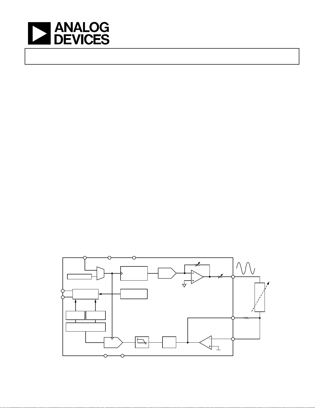
FUNCTIONAL BLOCK DIAGRAM
DDMCLK
OSCILLATOR
SCL
SDA
REGISTER
Rev. D
Information furnished by Analog Devices is believed to be accurate and reliable. However, no
responsibility is assumed by Anal og Devices for its use, nor for any infringements of patents or ot her
rights of third parties that may result from its use. Specifications subject to change without notice. No
license is granted by implication or otherwise under any patent or patent rights of Analog Devices.
Trademarks and registered trademarks are the property of their respective owners.
I2C
INTERFACE
REAL
IMAGINARY
REGIS TER
1024-POINT DFT
ADC
(12 BITS)
AGND DGND
DVDD
DDS
CORE
(27 BITS)
TEMPERATURE
SENSOR
AD5933
LPF
DAC
R
OUT
GAIN
VDD/2
Figure 1.
One Technology Way, P.O. Box 9106, Norwood, MA 02062-9106, U.S.A.
Tel: 781.329.4700 www.analog.com
Fax: 781.461.3113 ©2005–2011 Analog Devices, Inc. All rights reserved.
VOUT
Z(ω)
RFB
VIN
05324-001
Page 2

AD5933 Data Sheet
TABLE OF CONTENTS
Features.............................................................................................. 1
Applications....................................................................................... 1
General Description......................................................................... 1
Functional Block Diagram ..............................................................1
Revision History ...............................................................................3
Specifications..................................................................................... 4
I2C Serial Interface Timing Characteristics ..............................6
Absolute Maximum Ratings............................................................ 7
ESD Caution.................................................................................. 7
Pin Configuration and Descriptions.............................................. 8
Typical Performance Characteristics ............................................. 9
Terminology .................................................................................... 12
System Description......................................................................... 13
Transmit Stage............................................................................. 14
Frequency Sweep Command Sequence................................... 15
Receive Stage............................................................................... 15
DFT Operation ...........................................................................15
System Clock............................................................................... 16
Temperature Sensor ...................................................................16
Temperature Conversion Details.............................................. 16
Temperature Value Register ......................................................16
Temperature Conversion Formula........................................... 16
Impedance Calculation.................................................................. 17
Magnitude Calculation.............................................................. 17
Gain Factor Calculation ............................................................17
Impedance Calculation Using Gain Factor............................. 17
Gain Factor Variation with Frequency.................................... 17
Two-Point Calibration ............................................................... 18
Two-Point Gain Factor Calculation......................................... 18
Gain Factor Setup Configuration............................................. 18
Gain Factor Recalculation......................................................... 18
Gain Factor Temperature Variation......................................... 19
Impedance Error......................................................................... 19
Measuring the Phase Across an Impedance ........................... 19
Performing a Frequency Sweep ....................................................22
Register Map ................................................................................... 23
Control Register (Register Address 0x80, Register Address
0x81)............................................................................................. 23
Start Frequency Register (Register Address 0x82, Register
Address 0x83, Register Address 0x84)..................................... 24
Frequency Increment Register (Register Address 0x85,
Register Address 0x86, Register Address 0x87) .....................25
Number of Increments Register (Register Address 0x88,
Register Address 0x89).............................................................. 25
Number of Settling Time Cycles Register (Register Address
0x8A, Register Address 0x8B) ................................................. 25
Status Register (Register Address 0x8F).................................. 26
Temperature Data Register (16 Bits—Register Address 0x92,
Register Address 0x93).............................................................. 26
Real and Imaginary Data Registers (16 Bits—Register
Address 0x94, Register Address 0x95, Register Address 0x96,
Register Address 0x97).............................................................. 26
Serial Bus Interface......................................................................... 27
General I2C Timing.................................................................... 27
Writing/Reading to the AD5933.............................................. 28
Block Write.................................................................................. 28
Read Operations......................................................................... 29
Typical Applications....................................................................... 30
Measuring Small Impedances................................................... 30
Biomedical: Noninvasive Blood Impedance Measurement.. 32
Sensor/Complex Impedance Measurement............................ 32
Electro-Impedance Spectroscopy............................................. 33
Choosing a Reference for the AD5933........................................ 34
Layout and Configuration............................................................. 35
Power Supply Bypassing and Grounding................................ 35
Evaluation Board............................................................................ 36
Using the Evaluation Board ...................................................... 36
Prototyping Area........................................................................ 36
Crystal Oscillator (XO) vs. External Clock............................. 36
Schematics................................................................................... 37
Outline Dimensions....................................................................... 41
Ordering Guide .......................................................................... 41
Rev. D | Page 2 of 44
Page 3

Data Sheet AD5933
REVISION HISTORY
12/11—Rev. C to Rev. D
Changes to Impedance Error Section...........................................19
Removed Figure 26 and Figure 27;
Renumbered Sequentially ..............................................................19
Removed Figure 28, Figure 29, Figure 30, Figure 31..................20
Changes to Figure 39 ......................................................................37
Changes to Figure 40 ......................................................................38
Changes to Figure 41 ......................................................................39
Changes to Figure 42 ......................................................................40
8/10—Rev. B to Rev. C
Changes to Impedance Error Section...........................................19
Changes to Figure 45 ......................................................................38
Changes to U4 Description in Table 19........................................42
2/10—Rev. A to Rev. B
Changes to General Description.....................................................1
5/08—Rev. 0 to Rev. A
Changes to Layout.............................................................. Universal
Changes to Figure 1 ..........................................................................1
Changes to Table 1 ............................................................................4
Changes to Figure 17......................................................................13
Changes to System Description Section ......................................13
Changes to Figure 19......................................................................14
Changes to Figure 24......................................................................18
Changes to Impedance Error Section...........................................19
Added Measuring the Phase Across an Impedance Section .....21
Changes to Register Map Section .................................................24
Added Measuring Small Impedances Section.............................31
Changes to Table 18 ........................................................................35
Added Evaluation Board Section..................................................37
Changes to Ordering Guide...........................................................43
9/05—Revision 0: Initial Version
Rev. D | Page 3 of 44
Page 4

AD5933 Data Sheet
SPECIFICATIONS
VDD = 3.3 V, MCLK = 16.776 MHz, 2 V p-p output excitation voltage @ 30 kHz, 200 kΩ connected between Pin 5 and Pin 6; feedback
resistor = 200 kΩ connected between Pin 4 and Pin 5; PGA gain = ×1, unless otherwise noted.
Table 1.
Y Version1
Parameter
Min Typ Max
SYSTEM
Impedance Range 1 K 10 M Ω
Total System Accuracy 0.5 %
System Impedance Error Drift 30 ppm/°C
TRANSMIT STAGE
Output Frequency Range
2
1
100 kHz
Output Frequency Resolution 0.1 Hz
MCLK Frequency 16.776 MHz Maximum system clock frequency
Internal Oscillator Frequency3 16.776 MHz Frequency of internal clock
Internal Oscillator Temperature Coefficient 30 ppm/°C
TRANSMIT OUTPUT VOLTAGE
Range 1
AC Output Excitation Voltage
4
1.98 V p-p
DC Bias5 1.48 V
DC Output Impedance 200 Ω TA = 25°C
Short-Circuit Current to Ground at VOUT ±5.8 mA TA = 25°C
Range 2
AC Output Excitation Voltage4 0.97 V p-p See Figure 6
5
DC Bias
0.76 V
DC Output Impedance 2.4 kΩ
Short-Circuit Current to Ground at VOUT ±0.25 mA
Range 3
AC Output Excitation Voltage
5
DC Bias
4
0.383 V p-p See Figure 8
0.31 V
DC Output Impedance 1 kΩ
Short-Circuit Current to Ground at VOUT ±0.20 mA
Range 4
AC Output Excitation Voltage
5
DC Bias
4
0.198 V p-p See Figure 10
0.173 V
DC Output Impedance 600 Ω
Short-Circuit Current to Ground at VOUT ±0.15 mA
SYSTEM AC CHARACTERISTICS
Signal-to-Noise Ratio 60 dB
Total Harmonic Distortion −52 dB
Spurious-Free Dynamic Range
Wide Band (0 MHz to 1 MHz) −56 dB
Narrow Band (±5 kHz) −85 dB
Unit Test Conditions/Comments
100 Ω to 1 kΩ requires extra buffer
circuitry, see the Measuring Small
Impedances section
2 V p-p output excitation voltage at
30 kHz, 200 kΩ connected between
Pin 5 and Pin 6
<0.1 Hz resolution achievable using
DDS techniques
See Figure 4 for output voltage
distribution
DC bias of the ac excitation signal;
see Figure 5
DC bias of output excitation signal;
see Figure 7
DC bias of output excitation signal;
see Figure 9
DC bias of output excitation signal.
See Figure 11
Rev. D | Page 4 of 44
Page 5

Data Sheet AD5933
Y Version1
Parameter
Min Typ Max
RECEIVE STAGE
Input Leakage Current 1 nA To VIN pin
Input Capacitance
6
0.01 pF Pin capacitance between VIN and GND
Feedback Capacitance (CFB) 3 pF
ANALOG-TO-DIGITAL CONVERTER
Resolution
Sampling Rate
6
12 Bits
250 kSPS ADC throughput rate
TEMPERATURE SENSOR
Accuracy ±2.0 °C −40°C to +125°C temperature range
Resolution 0.03 °C
Temperature Conversion Time 800 s
LOGIC INPUTS
Input High Voltage (VIH) 0.7 × VDD
Input Low Voltage (VIL) 0.3 × VDD
Input Current
7
1 µA TA = 25°C
Input Capacitance 7 pF TA = 25°C
POWER REQUIREMENTS
VDD 2.7 5.5 V
IDD (Normal Mode ) 10 15 mA VDD = 3.3 V
17 25 mA VDD = 5.5 V
IDD (Standby Mode) 11 mA
16 mA VDD = 5.5 V
IDD (Power-Down Mode) 0.7 5 µA VDD = 3.3 V
1 8 µA VDD = 5.5 V
1
Temperature range for Y version = −40°C to +125°C, typical at 25°C.
2
The lower limit of the output excitation frequency can be lowered by scaling the clock supplied to the AD5933.
3
Refer to Figure 14, Figure 15, and Figure 16 for the internal oscillator frequency distribution with temperature.
4
The peak-to-peak value of the ac output excitation voltage scales with supply voltage according to the following formula:
Output Excitation Voltage (V p-p) = [2/3.3] × VDD
where VDD is the supply voltage.
5
The dc bias value of the output excitation voltage scales with supply voltage according to the following formula:
Output Excitation Bias Voltage (V) = [2/3.3] × VDD
where VDD is the supply voltage.
6
Guaranteed by design or characterization, not production tested. Input capacitance at the VOUT pin is equal to pin capacitance divided by open-loop gain of current-
to-voltage amplifier.
7
The accumulation of the currents into Pin 8, Pin 15, and Pin 16.
Unit Test Conditions/Comments
Feedback capacitance around currentto-voltage amplifier; appears in
parallel with feedback resistor
Conversion time of single temperature
measurement
VDD = 3.3 V; see the Control Register
(Register Address 0X80, Register
Address 0X81) section
Rev. D | Page 5 of 44
Page 6
AD5933 Data Sheet
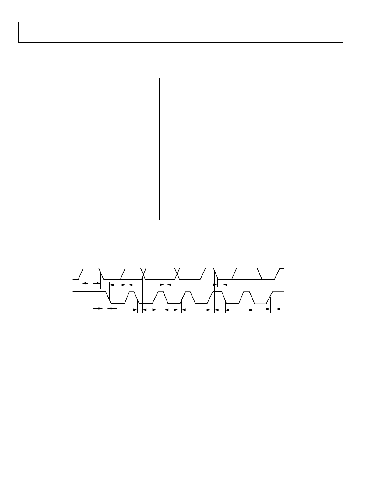
S
I2C SERIAL INTERFACE TIMING CHARACTERISTICS
VDD = 2.7 V to 5.5 V. All specifications T
MIN
to T
, unless otherwise noted.1
MAX
Table 2.
Parameter
f
400 kHz max SCL clock frequency
SCL
2
Limit at T
MIN
, T
MAX
Unit Description
t1 2.5 µs min SCL cycle time
t2 0.6 µs min t
t3 1.3 µs min t
t4 0.6 µs min t
t5 100 ns min t
3
t
6
0.9 µs max t
0 µs min t
t7 0.6 µs min t
t8 0.6 µs min t
t9 1.3 µs min t
, SCL high time
HIGH
, SCL low time
LOW
, start/repeated start condition hold time
HD, STA
, data setup time
SU, DAT
, data hold time
HD, DAT
, data hold time
HD, DAT
, setup time for repeated start
SU, STA
, stop condition setup time
SU, STO
, bus free time between a stop and a start condition
BUF
t10 300 ns max tF, rise time of SDA when transmitting
0 ns min tR, rise time of SCL and SDA when receiving (CMOS compatible)
t11 300 ns max tF, fall time of SCL and SDA when transmitting
0 ns min tF, fall time of SDA when receiving (CMOS compatible)
250 ns max tF, fall time of SDA when receiving
20 + 0.1 C
4
b
ns min tF, fall time of SCL and SDA when transmitting
Cb 400 pF max Capacitive load for each bus line
1
See Figure 2.
2
Guaranteed by design and characterization, not production tested.
3
A master device must provide a hold time of at least 300 ns for the SDA signal (referred to V
4
Cb is the total capacitance of one bus line in picofarads. Note that tR and tF are measured between 0.3 VDD and 0.7 VDD.
of the SCL signal) to bridge the undefined falling edge of SCL.
IH MIN
DA
t
SCL
9
START
CONDITION
t
3
t
4
t
10
t
6
t
11
Figure 2. I
t
2
2
C Interface Timing Diagram
t
t
5
7
t
4
REPEATED
START
CONDITIO N
t
1
t
8
STOP
CONDITIO N
05324-002
Rev. D | Page 6 of 44
Page 7
Data Sheet AD5933
ABSOLUTE MAXIMUM RATINGS
TA = 25°C, unless otherwise noted.
Table 3.
Parameter Rating
DVDD to GND −0.3 V to +7.0 V
AVDD1 to GND −0.3 V to +7.0 V
AVDD2 to GND −0.3 V to +7.0 V
SDA/SCL to GND −0.3 V to VDD + 0.3 V
VOUT to GND −0.3 V to VDD + 0.3 V
VIN to GND −0.3 V to VDD + 0.3 V
MCLK to GND −0.3 V to VDD + 0.3 V
Operating Temperature Range
Extended Industrial (Y Grade) −40°C to +125°C
Storage Temperature Range −65°C to +160°C
Maximum Junction Temperature 150°C
SSOP Package, Thermal Impedance
θJA 139°C/W
θJC 136°C/W
Reflow Soldering (Pb-Free)
Peak Temperature 260°C
Time at Peak Temperature 10 sec to 40 sec
Stresses above those listed under Absolute Maximum Ratings
may cause permanent damage to the device. This is a stress
rating only; functional operation of the device at these or any
other conditions above those indicated in the operational
section of this specification is not implied. Exposure to absolute
maximum rating conditions for extended periods may affect
device reliability.
ESD CAUTION
Rev. D | Page 7 of 44
Page 8
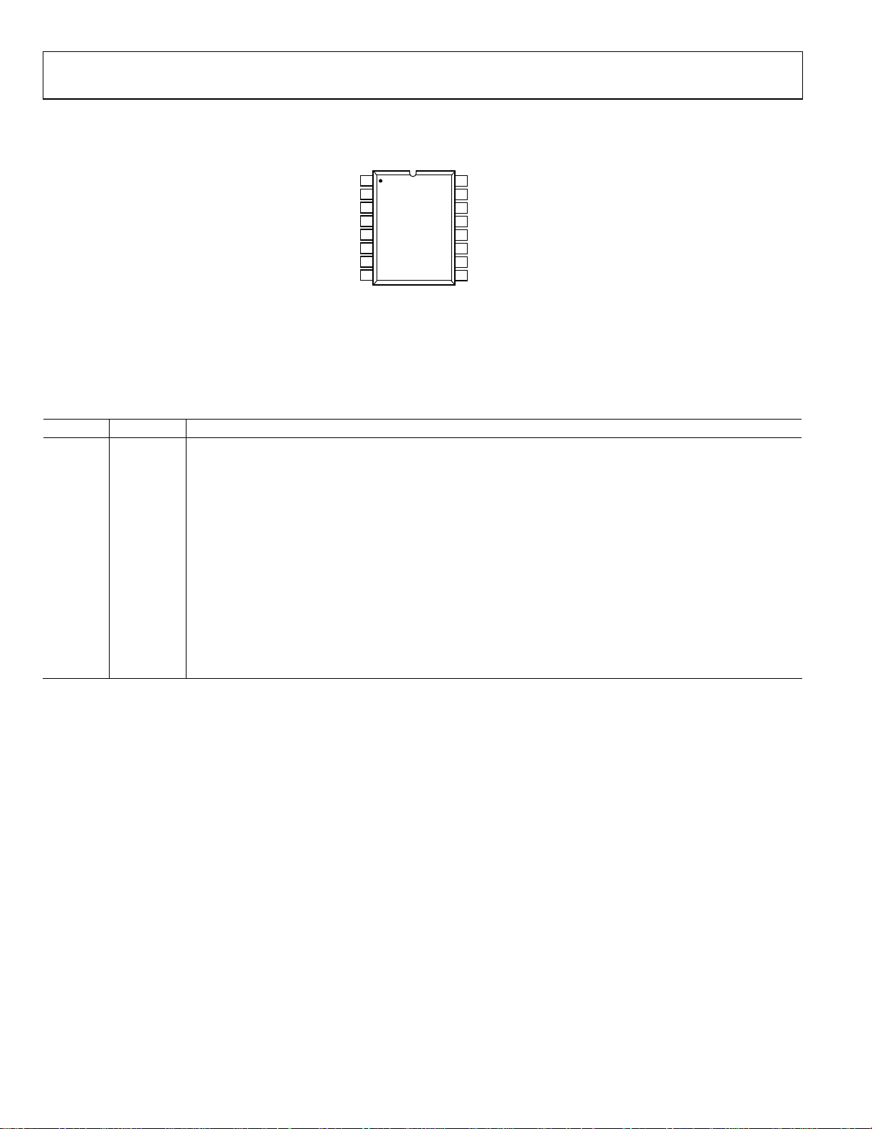
AD5933 Data Sheet
PIN CONFIGURATION AND DESCRIPTIONS
NC
1
NC
2
NC
3
RFB
VIN
VOUT
NC
MCLK
NOTES:
IT IS RECO MMENDED TO TIE ALL SUPPLY
1.
CONNECTIONS (PIN 9, PIN 10, AND PIN 11)
AND RUN FROM A SINGLE SUPPLY BETWEEN
2.7V AND 5.5V. IT IS ALSO RECOMMENDED TO
CONNECT ALL GROUND SIGNALS TOGETHER
(PIN 12, PI N 13, AND PIN 14).
AD5933
4
TOP VIEW
5
(Not to Scale)
6
7
8
NC = NO CONNECT
Figure 3. Pin Configuration
Table 4. Pin Function Descriptions
Pin No. Mnemonic Description
1, 2, 3, 7 NC No Connect.
4 RFB
External Feedback Resistor. Connected from Pin 4 to Pin 5 and used to set the gain of the current-to-voltage
amplifier on the receive side.
5 VIN Input to Receive Transimpedance Amplifier. Presents a virtual earth voltage of VDD/2.
6 VOUT Excitation Voltage Signal Output.
8 MCLK The master clock for the system is supplied by the user.
9 DVDD Digital Supply Voltage.
10 AVDD1 Analog Supply Voltage 1.
11 AVDD2 Analog Supply Voltage 2.
12 DGND Digital Ground.
13 AGND1 Analog Ground 1.
14 AGND2 Analog Ground 2.
15 SDA I2C Data Input. Open-drain pins requiring 10 kΩ pull-up resistors to VDD.
16 SCL I2C Clock Input. Open-drain pins requiring 10 kΩ pull-up resistors to VDD.
16
15
14
13
12
11
10
9
SCL
SDA
AGND2
AGND1
DGND
AVDD2
AVDD1
DVDD
05324-003
Rev. D | Page 8 of 44
Page 9
Data Sheet AD5933
TYPICAL PERFORMANCE CHARACTERISTICS
35
30
25
20
15
NUMBER OF DEVICES
10
MEAN = 1.9824
SIGMA = 0.0072
30
25
20
15
10
NUMBER OF DEVI CES
MEAN = 0.7543
SIGMA = 0.0099
5
0
1.92 1.94 1.96 1.98 2.00 2. 02 2.04
VOLTAGE (V)
2.06
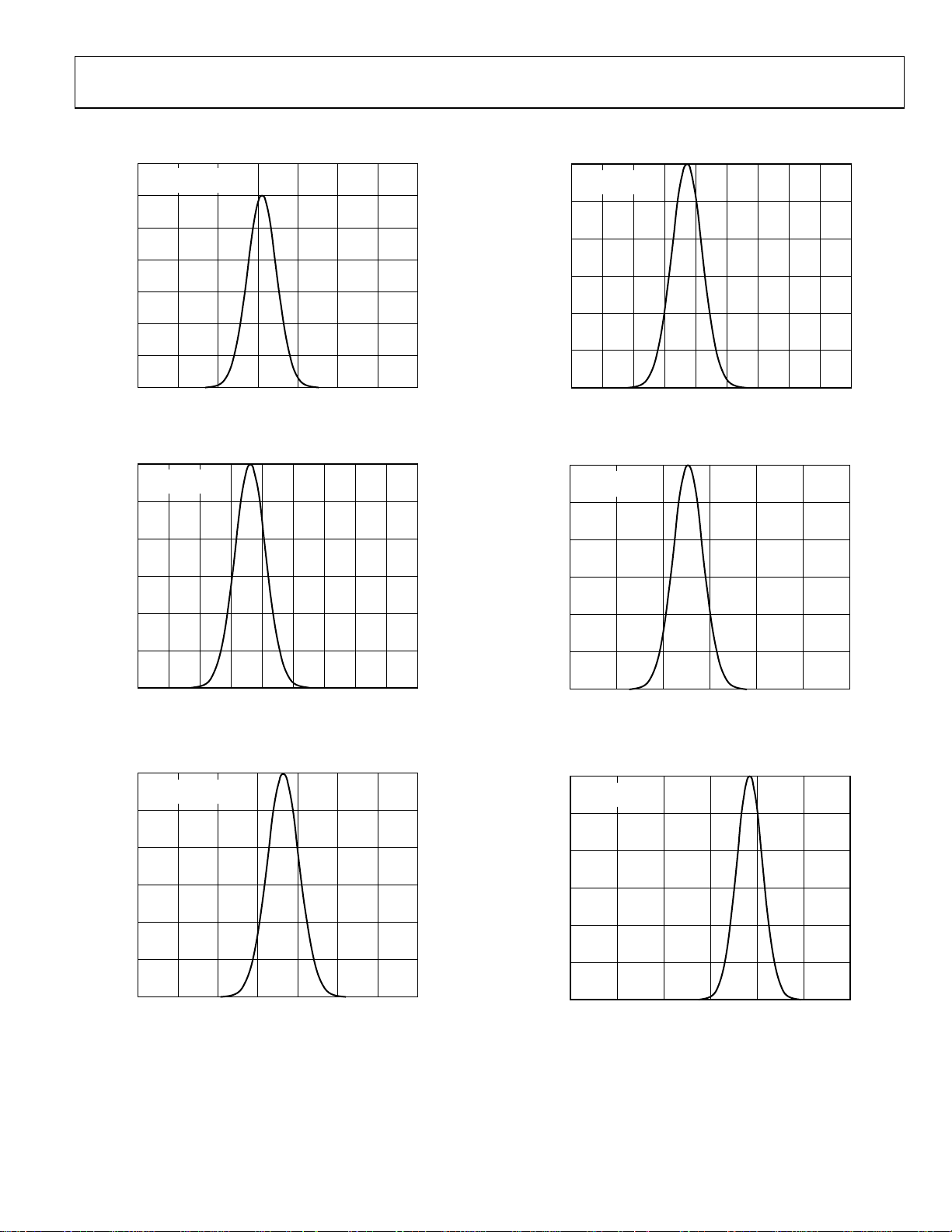
Figure 4. Range 1 Output Excitation Voltage Distribution, VDD = 3.3 V
30
MEAN = 1.4807
SIGMA = 0.0252
25
20
15
10
NUMBER OF DEVI CES
5
0
1.30
1.35 1.40 1.45 1.50 1.55 1.60 1.65 1.70
VOLTAGE (V)
1.75
Figure 5. Range 1 DC Bias Distribution, VDD = 3.3 V
30
MEAN = 0.9862
SIGMA = 0.0041
25
5
0
0.68
0.70 0.72 0.74 0.76 0.78 0.80 0.82 0.84
05324-004
VOLTAGE (V)
0.86
05324-007
Figure 7. Range 2 DC Bias Distribution, VDD = 3.3 V
30
MEAN = 0.3827
SIGMA = 0.00167
25
20
15
10
NUMBER OF DEVICES
5
0
0.370
05324-005
0.375 0. 380 0.385 0.390 0.395
VOLTAGE (V)
0.400
05324-008
Figure 8. Range 3 Output Excitation Voltage Distribution, VDD = 3.3 V
30
MEAN = 0.3092
SIGMA = 0.0014
25
20
15
10
NUMBER OF DEVI CES
5
0
0.95 0.96 0.97 0.98 0.99 1. 00 1.01 1.02
VOLTAGE (V)
Figure 6. Range 2 Output Excitation Voltage Distribution, VDD = 3.3 V
05324-006
Rev. D | Page 9 of 44
20
15
10
NUMBER OF DEVI CES
5
0
0.290
0.295 0. 300 0.305 0.310 0.315
VOLTAGE (V)
Figure 9. Range 3 DC Bias Distribution, VDD = 3.3 V
0.320
05324-009
Page 10
AD5933 Data Sheet
30
MEAN = 0.1982
SIGMA = 0.0008
25
20
15
10
NUMBER OF DEVICES
5
0
0.192 0.194 0.196 0.198 0.200 0.202 0.204 0.206
VOLTAGE (V)
Figure 10. Range 4 Output Excitation Voltage Distribution, VDD = 3.3 V
30
MEAN = 0.1792
SIGMA = 0.0024
25
20
15
10
NUMBER OF DEVICES
5
15.8
AVDD1, AVDD2, DVDD CONNECTED TOG ETHER.
OUTPUT EXCITAT ION FREQUENCY = 30kHz
15.3
RFB, Z
14.8
14.3
13.8
13.3
IDD (mA)
12.8
12.3
11.8
11.3
10.8
05324-010
CALIBR AT ION
0
246810121416
= 100kΩ
MCLK FREQUENCY (MHz)
18
05324-012
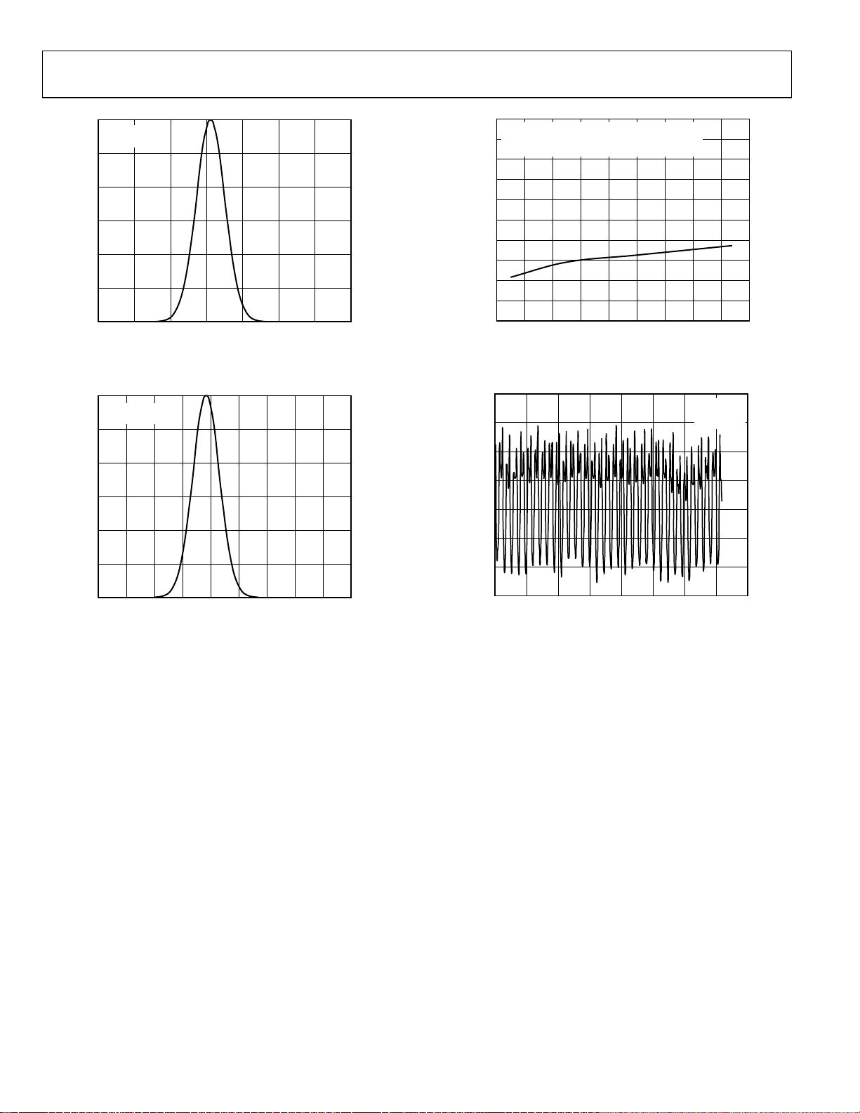
Figure 12. Typical Supply Current vs. MCLK Frequency
0.4
0.2
0
–0.2
–0.4
–0.6
PHASE ERROR (Degrees)
–0.8
VDD = 3.3V
= 25°C
T
A
f = 32kHz
0
0.160
0.165 0.170 0.175 0.180 0.185 0.190 0.195 0. 200
VOLTAGE (V)
Figure 11. Range 4 DC Bias Distribution, VDD = 3.3 V
0.205
–1.0
0
50 100 150 200 250 300 350
05324-011
PHASE (Degrees)
400
05324-013
Figure 13. Typical Phase Error
Rev. D | Page 10 of 44
Page 11
Data Sheet AD5933
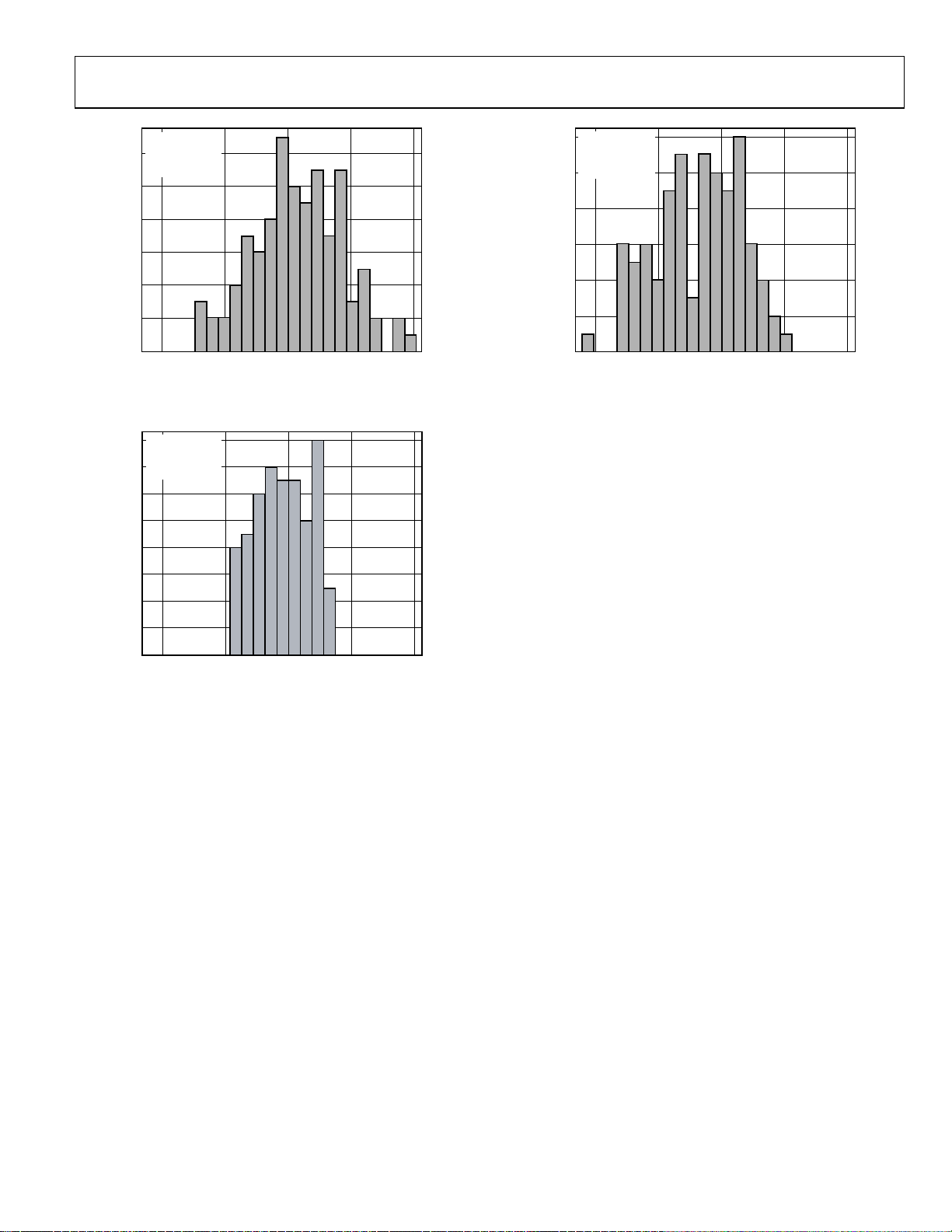
12
N = 106
MEAN = 16.8292
12
SD = 0.142904
TEMP = –40°C
10
8
6
COUNT
4
N = 100
MEAN = 16.7257
SD = 0.137633
TEMP = 125°C
10
8
6
COUNT
4
2
0
16.4 16.6 16.8 17. 0
OSCILLATOR FREQUENCY (MHz)
17.2
05324-014
2
0
16.4 16.6 16.8 17. 0
OSCILLATOR FREQUENCY (MHz)
Figure 14. Frequency Distribution of Internal Oscillator at −40°C Figure 16. Frequency Distribution of Internal Oscillator at 125°C
16
N = 100
MEAN = 16.78 11
SD = 0.0881565
14
TEMP = 25°C
12
10
8
COUNT
6
4
2
0
16.4 16.6 16.8 17. 0
OSCILLATOR FREQUENCY (MHz)
17.2
05324-015
Figure 15. Frequency Distribution of Internal Oscillator at 25°C
17.2
05324-016
Rev. D | Page 11 of 44
Page 12

AD5933 Data Sheet
TERMINOLOGY
Tot a l S ys t em A cc ur ac y
The AD5933 can accurately measure a range of impedance
values to less than 0.5% of the correct impedance value for
supply voltages between 2.7 V to 5.5 V.
Spurious-Free Dynamic Range (SFDR)
Along with the frequency of interest, harmonics of the fundamental frequency and images of these frequencies are present at
the output of a DDS device. The spurious-free dynamic range
refers to the largest spur or harmonic present in the band of
interest. The wideband SFDR gives the magnitude of the largest
harmonic or spur relative to the magnitude of the fundamental
frequency in the 0 Hz to Nyquist bandwidth. The narrow-band
SFDR gives the attenuation of the largest spur or harmonic in a
bandwidth of ±200 kHz, about the fundamental frequency.
Signal-to-Noise Ratio (SNR)
SNR is the ratio of the rms value of the measured output signal
to the rms sum of all other spectral components below the
Nyquist frequency. The value for SNR is expressed in decibels.
Total Harmonic Distortion (THD)
THD is the ratio of the rms sum of harmonics to the fundamental, where V1 is the rms amplitude of the fundamental
and V2, V3, V4, V5, and V6 are the rms amplitudes of the
second through the sixth harmonics. For the AD5933, THD
is defined as
22222
5
+++
THD
log20(dB)
=
V1
V6VV4V3V2
Rev. D | Page 12 of 44
Page 13
Data Sheet AD5933
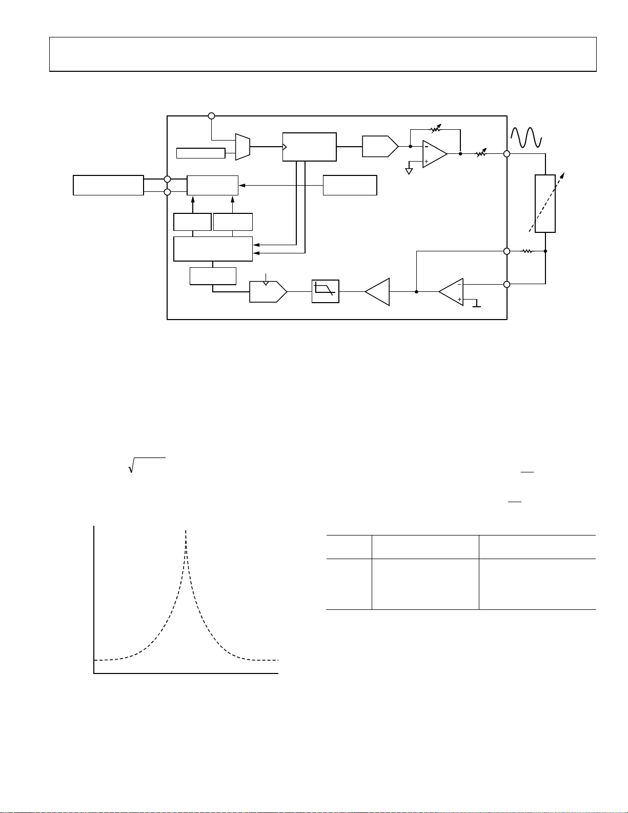
SYSTEM DESCRIPTION
MCLK
DDS
MICROCONTRO LLER
SCL
SDA
OSCILLATOR
I2C
INTERFACE
CORE
(27 BITS)
COS SIN
TEMPERATURE
SENSOR
DAC
R
OUT
VOUT
Z(ω)
REAL
REGISTER
IMAGINARY
REGISTER
MAC CORE
(1024 DFT)
WINDOWI NG
OF DATA
MCLK
ADC
(12 BITS)
Figure 17. Block Overview
The AD5933 is a high precision impedance converter system
solution that combines an on-board frequency generator with a
12-bit, 1 MSPS ADC. The frequency generator allows an external
complex impedance to be excited with a known frequency. The
response signal from the impedance is sampled by the on-board
ADC and DFT processed by an on-board DSP engine. The DFT
algorithm returns both a real (R) and imaginary (I) data-word at
each frequency point along the sweep. The impedance magnitude
and phase are easily calculated using the following equations:
22
IRMagnitude +=
Phase
= tan−1(I/R)
To characterize an impedance profile Z(
ω), generally a frequency
sweep is required, like that shown in Figure 18.
IMPEDANCE
FREQUENCY
Figure 18. Impedance vs. Frequency Profile
05324-018
AD5933
RFB
PROGRAMMABLE
LPF
GAIN AMPLIFIER
×5
×1
VDD/2
VIN
The AD5933 permits the user to perform a frequency sweep with
a user-defined start frequency, frequency resolution, and number
of points in the sweep. In addition, the device allows the user to
program the peak-to-peak value of the output sinusoidal signal as
an excitation to the external unknown impedance connected
between the VOUT and VIN pins.
Table 5 gives the four possible output peak-to-peak voltages and
the corresponding dc bias levels for each range for 3.3 V. These
values are ratiometric with VDD. So for a 5 V supply
98.1 −=×=1RangeforVoltageExcitationOutput
48.1 −=×=1RangeforVoltageBiasDCOutput
0.5
3.3
0.5
3.3
Table 5. Voltage Levels Respective Bias Levels for 3.3 V
Output Excitation
Range
Voltage Amplitude Output DC Bias Level
1 1.98 V p-p 1.48 V
2 0.97 V p-p 0.76 V
3 383 mV p-p
0.31 V
4 198 mV p-p 0.173 V
The excitation signal for the transmit stage is provided on-chip
using DDS techniques that permit subhertz resolution. The receive
stage receives the input signal current from the unknown impedance,
performs signal processing, and digitizes the result. The clock for
the DDS is generated from either an external reference clock,
which is provided by the user at MCLK, or by the internal
oscillator. The clock for the DDS is determined by the status of
Bit D3 in the control register (see Register Address 0x81 in the
Register Map section).
05324-017
ppV3
ppV24.2
Rev. D | Page 13 of 44
Page 14

AD5933 Data Sheet
=
TRANSMIT STAGE
As shown in Figure 19, the transmit stage of the AD5933 is made
up of a 27-bit phase accumulator DDS core that provides the
output excitation signal at a particular frequency. The input to
the phase accumulator is taken from the contents of the start
frequency register (see Register Address 0x82, Register Address
0x83, and Register Address 0x84). Although the phase accumulator offers 27 bits of resolution, the start frequency register has
the three most significant bits (MSBs) set to 0 internally; therefore,
the user has the ability to program only the lower 24 bits of the
start frequency register.
R(GAIN)
PHASE
ACCUMULATOR
(27 BITS)
The AD5933 offers a frequency resolution programmable by the
user down to 0.1 Hz. The frequency resolution is programmed
via a 24-bit word loaded serially over the I
frequency increment register.
The frequency sweep is fully described by the programming of
three parameters: the start frequency, the frequency increment,
and the number of increments.
Start Frequency
This is a 24-bit word that is programmed to the on-board RAM
at Register Address 0x82, Register Address 0x83, and Register
Address 0x84 (see the Register Map section). The required code
loaded to the start frequency register is the result of the formula
shown in Equation 1, based on the master clock frequency and the
required start frequency output from the DDS.
⎛
⎜
⎜
⎜
⎜
⎝
⎛
⎜
⎝
For example, if the user requires the sweep to begin at 30 kHz and
has a 16 MHz clock signal connected to MCLK, the code that
needs to be programmed is given by
The user programs the value of 0x0F to Register Address 0x82, the
value of 0x5C to Register Address 0x83, and the value of 0x28 to
Register Address 0x84.
DAC
V
BIAS
Figure 19. Transmit Stage
=
CodeFrequencyStart
FrequencyStartOutputRequired
MCLK
⎞
⎟
⎠
⎛
⎜
kHz30
⎜
=CodeFrequencyStart
⎜
MHz16
⎛
⎜
⎜
⎜
4
⎝
⎝
VOUT
5324-019
2
C interface to the
⎞
⎟
(1)
27
⎟
24×
⎟
⎟
⎠
⎞
⎟
⎟
27
0x0F5C282
≡×
⎟
⎞
⎟
⎟
⎟
⎠
⎠
Frequency Increment
This is a 24-bit word that is programmed to the on-board RAM
at Register Address 0x85, Register Address 0x86, and Register
Address 0x87 (see the Register Map). The required code loaded
to the frequency increment register is the result of the formula
shown in Equation 2, based on the master clock frequency and the
required increment frequency output from the DDS.
CodeIncrementFrequency
⎛
⎜
Re
⎜
⎜
⎜
⎝
MCLK
⎛
⎜
⎝
IncrementFrequencyquired
⎞
⎟
4
⎠
⎞
⎟
(2)
27
⎟
×
2
⎟
⎟
⎠
For example, if the user requires the sweep to have a resolution
of 10 Hz and has a 16 MHz clock signal connected to MCLK, the
code that needs to be programmed is given by
⎛
⎜
⎜
=CodeIncrementFrequency
⎜
⎛
⎜
⎜
⎜
⎝
⎝
⎞
⎟
Hz10
⎟
0x00014F
≡
⎟
MHz16
⎞
⎟
⎟
⎟
4
⎠
⎠
The user programs the value of 0x00 to Register Address 0x85,
the value of 0x01 to Register Address 0x86, and the value of 0x4F
to Register Address 0x87.
Number of Increments
This is a 9-bit word that represents the number of frequency
points in the sweep. The number is programmed to the on-board
RAM at Register Address 0x88 and Register Address 0x89 (see the
Register Map section). The maximum number of points that can
be programmed is 511.
For example, if the sweep needs 150 points, the user programs
the value of 0x00 to Register Address 0x88 and the value of 0x96
to Register Address 0x89.
Once the three parameter values have been programmed, the
sweep is initiated by issuing a start frequency sweep command to
the control register at Register Address 0x80 and Register Address
0x81 (see the Register Map section). Bit D2 in the status register
(Register Address 0x8F) indicates the completion of the frequency
measurement for each sweep point. Incrementing to the next
frequency sweep point is under the control of the user. The
measured result is stored in the two register groups that follow:
0x94, 0x95 (real data) and 0x96, 0x97 (imaginary data) that should
be read before issuing an increment frequency command to the
control register to move to the next sweep point. There is the
facility to repeat the current frequency point measurement by
issuing a repeat frequency command to the control register. This
has the benefit of allowing the user to average successive readings.
When the frequency sweep has completed all frequency points,
Bit D3 in the status register is set, indicating completion of the
sweep
. Once this bit is set, further increments are disabled.
Rev. D | Page 14 of 44
Page 15

Data Sheet AD5933
V
FREQUENCY SWEEP COMMAND SEQUENCE RECEIVE STAGE
The following sequence must be followed to implement a
frequency sweep:
1. Enter standby mode. Prior to issuing a start frequency sweep
command, the device must be placed in a standby
mode by
issuing an enter standby mode command to the control
register (Register Address 0x80 and Register Address 0x81).
In this mode, the VOUT and VIN pins are connected
internally to ground so there is no dc bias across the external
impedance or between the impedance and ground.
2. Enter initialize
mode. In general, high Q complex circuits
require a long time to reach steady state. To facilitate the
measurement of such impedances, this mode allows the user
full control of the settling time requirement before entering
start frequency sweep
measurement takes place.
mode where the impedance
An initialize with a start frequency command to the control
register enters initialize mode. In this mode the impedance
is excited with the programmed start frequency, but no measurement takes place. The user times out the required settling
time before issuing a start frequency sweep command to the
control register to enter the start frequency sweep mode.
3. Enter start frequency sweep
mode. The user enters this mode
by issuing a start frequency sweep command to the control
register. In this mode, the ADC starts measuring after the
programmed number of settling time cycles has elapsed. The
user can program an integer number of output frequency
cycles (settling time cycles)
to Register Address 0x8A and
Register Address 0x8B before beginning the measurement
at each frequency point (see Figure 28).
The DDS output signal is passed through a programmable gain
stage to generate the four ranges of peak-to-peak output excitation
signals listed in Tabl e 5. The peak-to-peak output excitation voltage is selected by setting Bit D10 and Bit D9 in the control register
(see the Control Register (Register Address 0X80, Register
Address 0X81) section) and is made available at the VOUT pin.
The receive stage comprises a current-to-voltage amplifier,
followed by a programmable gain amplifier (PGA), antialiasing
filter, and ADC. The receive stage schematic is shown in
Figure 20. The unknown impedance is connected between the
VOUT and VIN pins. The first stage current-to-voltage amplifier
configuration means that a voltage present at the VIN pin is a
virtual ground with a dc value set at VDD/2. The signal current
that is developed across the unknown impedance flows into the
VIN pin and develops a voltage signal at the output of the currentto-voltage converter. The gain of the current-to voltage amplifier
is determined by a user-selectable feedback resistor connected
between Pin 4 (RFB) and Pin 5 (VIN). It is important for the user
to choose a feedback resistance value that, in conjunction with the
selected gain of the PGA stage, maintains the signal within the
linear range of the ADC (0 V to VDD).
The PGA allows the user to gain the output of the current-tovoltage amplifier by a factor of 5 or 1, depending upon the status
of Bit D8 in the control register (see the Register Map section,
Register Address 0x80). The signal is then low-pass filtered and
presented to the input of the 12-bit, 1 MSPS ADC.
RFB
R
5 × R
R
LPF
ADC
05324-020
IN
C
R
VDD/2
Figure 20. Receive Stage
The digital data from the ADC is passed directly to the DSP core
of the AD5933, which performs a DFT on the sampled data.
DFT OPERATION
A DFT is calculated for each frequency point in the sweep. The
AD5933 DFT algorithm is represented by
1023
∑
n
=
0
−=
)))sin())(cos((()(
njnnxfX
where:
X(f) is the power in the signal at the Frequency Point f.
x(n) is the ADC output.
cos(n) and sin(n) are the sampled test vectors provided by the
DDS core at the Frequency Point f.
The multiplication is accumulated over 1024 samples for each
frequency point. The result is stored in two, 16-bit registers
representing the real and imaginary components of the result.
The data is stored in twos complement format.
Rev. D | Page 15 of 44
Page 16

AD5933 Data Sheet
SYSTEM CLOCK
The system clock for the AD5933 can be provided in one of two
ways. The user can provide a highly accurate and stable system
clock at the external clock pin (MCLK). Alternatively, the AD5933
provides an internal clock with a typical frequency of 16.776 MHz
by means of an on-chip oscillator.
The user can select the preferred system clock by programming
Bit D3 in the control register (Register Address 0x81, see
Table 11 ). The default clock option on power-up is selected to
be the internal oscillator.
The frequency distribution of the internal clock with temperature
can be seen in Figure 14, Figure 15, and Figure 16.
TEMPERATURE SENSOR
The temperature sensor is a 13-bit digital temperature sensor with
th
a 14
bit that acts as a sign bit. The on-chip temperature sensor
allows an accurate measurement of the ambient device temperature to be made.
The measurement range of the sensor is −40°C to +125°C. At
+150°C, the structural integrity of the device starts to deteriorate
when operated at voltage and temperature maximum specifications. The accuracy within the measurement range is ±2°C.
TEMPERATURE CONVERSION DETAILS
The conversion clock for the part is internally generated; no
external clock is required except when reading from and writing
to the serial port. In normal mode, an internal clock oscillator
runs an automatic conversion sequence.
The temperature sensor block defaults to a power-down state.
To perform a measurement, a measure temperature command
is issued by the user to the control register (Register Address 0x80
and Register Address 0x81). After the temperature operation is
complete (typically 800 s later), the block automatically
powers down until the next temperature command is issued.
The user can poll the status register (Register Address 0x8F) to see
if a valid temperature conversion has taken place, indicating that
valid temperature data is available to read at Register Address
0x92 and Register Address 0x93 (see the Register Map section).
TEMPERATURE VALUE REGISTER
The temperature value register is a 16-bit, read-only register that
stores the temperature reading from the ADC in 14-bit, twos
complement format. The two MSB bits are don’t cares. D13 is the
sign bit. The internal temperature sensor is guaranteed to a low
value limit of –40°C and a high value limit of +150°C. The digital
output stored in Register Address 0x92 and Register Address 0x93
for the various temperatures is outlined in Tabl e 6. The temperature sensor transfer characteristic is shown in Figure 21.
Table 6. Temperature Data Format
Temperature Digital Output D13…D0
−40°C 11, 1011, 0000, 0000
−30°C 11, 1100, 0100, 0000
−25°C 11, 1100, 1110, 0000
−10°C 11, 1110, 1100, 0000
−0.03125°C 11, 1111, 1111, 1111
0°C 00, 0000, 0000, 0000
+0.03125°C 00, 0000, 0000, 0001
+10°C 00, 0001, 0100, 0000
+25°C 00, 0011, 0010, 0000
+50°C 00, 0110, 0100, 0000
+75°C 00, 1001, 0110, 0000
+100°C 00, 1100, 1000, 0000
+125°C 00, 1111, 1010, 0000
+150°C 01, 0010, 1100, 0000
TEMPERATURE CONVERSION FORMULA
Positive Temperature = ADC Code (D)/32
Negative Temperature = (ADC Code (D)
where ADC Code uses all 14 bits of the data byte, including the
sign bit.
Negative Temperature = (ADC Code (D)
where ADC Code (D) is D13, the sign bit, and is removed from the
ADC code.)
01, 0010, 1100, 0000
00, 1001, 0 110, 0000
00, 0000, 0000, 0001
–0.03125°C
–40°C
–30°C
DIGITAL OUT PUT
11, 1111, 1111, 1111
11, 1100, 0100, 0000
11, 1011, 0000, 0000
Figure 21. Temperature Sensor Transfer Function
– 16384)/32
– 8192)/32
75°C
TEMPERATURE (°C)
150°C
05324-021
Rev. D | Page 16 of 44
Page 17

Data Sheet AD5933
IMPEDANCE CALCULATION
1
MAGNITUDE CALCULATION
The first step in impedance calculation for each frequency point
is to calculate the magnitude of the DFT at that point.
The DFT magnitude is given by
22
IRMagnitude +=
where:
R is the real number stored at Register Address 0x94 and
Register Address 0x95.
I is the imaginary number stored at Register Address 0x96 and
Register Address 0x97.
For example, assume the results in the real data and imaginary
data registers are as follows at a frequency point:
Real data register = 0x038B = 907 decimal
Imaginary data register = 0x0204 = 516 decimal
22
=+=Magnitude
506.1043)516907(
To convert this number into impedance, it must be multiplied
by
a scaling factor called the gain factor. The gain factor is
calculated during the calibration of the system with a known
impedance connected between the VOUT and VIN pins.
Once the gain factor has been calculated, it can be used in the
calculation of any unknown impedance between the VOUT and
VIN pins.
GAIN FACTOR CALCULATION
An example of a gain factor calculation follows, with the
following assumptions:
Output excitation voltage = 2 V p-p
Calibration impedance value, Z
CALIBRATION
PGA Gain = ×1
Current-to-voltage amplifier gain resistor = 200 kΩ
Calibration frequency = 30 kHz
Then typical contents of the real data and imaginary data
registers after a frequency point conversion are:
Real data register = 0xF064 = −3996 decimal
Imaginary data register = 0x227E = +8830 decimal
= 200 kΩ
22
=+−=Magnitude
106.9692)8830()3996(
⎛
⎜
⎜
=FactorGain
⎜
⎜
⎝
IMPEDANCE CALCULATION USING GAIN FACTOR
The next example illustrates how the calculated gain factor
derived previously is used to measure an unknown impedance.
For this example, assume that the unknown impedance = 510
kΩ.
After measuring the unknown impedance at a frequency of
30 kHz, assume that the real data and imaginary data registers
contain the following data:
Real data register = 0xFA3F = −1473 decimal
Imaginary data register = 0x0DB3 = +3507 decimal
Then the measured impedance at the frequency point is given
by
Impedance
=
=
GAIN FACTOR VARIATION WITH FREQUENCY
Because the AD5933 has a finite frequency response, the gain
factor also shows a variation with frequency. This variation in
gain factor results in an error in the impedance calculation over
a frequency range. Figure 22 shows an impedance profile based
on a single-point gain factor calculation. To minimize this error,
the frequency sweep should be limited to as small a frequency
range as possible.
101.5
VDD = 3.3V
CALIBRATION FREQUENCY = 60kHz
T
= 25°C
A
101.0
MEASURED CALIBR ATION IMPEDANCE = 100kΩ
100.5
100.0
IMPEDANCE (kΩ)
99.5
⎞
⎟
k200
Ω
⎟
=
⎟
106.9692
⎟
12-
10 × 515.819
⎠
22
1
MagnitudeFactorGain ×
863.3802))3507()1473((
=+−=Magnitude
1
−
12
××
863.380210819273.515
Ω=Ω
k791.509
⎛
⎜
⎜
FactorGain
⎜
Code
⎝
Admittance
⎛
=
⎞
⎝
=
⎟
⎠
Impedance
Magnitude
⎞
1
⎟
⎟
⎠
99.0
98.5
54
Figure 22. Impedance Profile Using a Single-Point Gain Factor Calculation
56 58 60 62 64
FREQUENCY (kHz)
66
05324-022
Rev. D | Page 17 of 44
Page 18

AD5933 Data Sheet
V
TWO-POINT CALIBRATION
Alternatively, it is possible to minimize this error by assuming
that the frequency variation is linear and adjusting the gain
factor with a two-point calibration. Figure 23 shows an
impedance profile based on a two-point gain factor calculation.
101.5
VDD = 3.3V
CALIBRATION F REQUENCY = 60kHz
T
= 25°C
A
101.0
MEASURED CALIBR ATION IMPEDANCE = 100kΩ
100.5
100.0
IMPEDANCE (kΩ)
99.5
99.0
98.5
54
Figure 23. Impedance Profile Using a Two-Point Gain Factor Calculation
56 58 60 62 64
FREQUE NCY (kHz )
66
05324-023
TWO-POINT GAIN FACTOR CALCULATION
This is an example of a two-point gain factor calculation
assuming the following:
Output excitation voltage = 2 V (p-p)
Calibration impedance value, Z
PGA gain = ×1
Supply voltage = 3.3 V
Current-to-voltage amplifier gain resistor = 100 kΩ
Calibration frequencies = 55 kHz and 65 kHz
Typical values of the gain factor calculated at the two calibration
frequencies read
Gain factor calculated at 55 kHz is 1.031224E-09
Gain factor calculated at 65 kHz is 1.035682E-09
Difference in gain factor (∆GF) is 1.035682E-09 −
1.031224E-09 = 4.458000E-12
Frequency span of sweep (∆F) = 10 kHz
Therefore, the gain factor required at 60 kHz is given by
= 100.0 kΩ
UNKNOWN
GAIN FACTOR SETUP CONFIGURATION
When calculating the gain factor, it is important that the receive
stage operate in its linear region. This requires careful selection
of the excitation signal range, current-to-voltage gain resistor,
and PGA gain.
CURRENT-TO-VOLTAGE
GAIN SETTING RESISTOR
RFB
Z
OUT
UNKNOWN
VDD/2
VIN
PGA
(×1 OR ×5)
Figure 24. System Voltage Gain
LPF
ADC
The gain through the system shown in Figure 24 is given by
RangeVoltageExcitationOuput
×
sistorSettingGain
Z
UNKNOWN
Re
GainPGA
×
For this example, assume the following system settings:
VDD = 3.3 V
Gain setting resistor = 200 kΩ
UNKNOWN
= 200 kΩ
Z
PGA setting = ×1
The peak-to-peak voltage presented to the ADC input is
2 V p-p. However, if a PGA gain of ×5 was chose, the voltage
would saturate the ADC.
GAIN FACTOR RECALCULATION
The gain factor must be recalculated for a change in any of the
following parameters:
•
Current-to-voltage gain setting resistor
Output excitation voltage
•
•
PGA gain
05324-024
⎛
⎜
⎜
⎝
12-E458000.4
kHz10
×
⎞
⎟
⎟
⎠
9-
10031224.1kHz5
×+
The required gain factor is 1.033453E-9.
The impedance is calculated as previously described.
Rev. D | Page 18 of 44
Page 19

Data Sheet AD5933
GAIN FACTOR TEMPERATURE VARIATION
The typical impedance error variation with temperature is in
the order of 30 ppm/°C. Figure 25 shows an impedance profile
with a variation in temperature for 100 kΩ impedance using a
two-point gain factor calibration.
101.5
VDD = 3.3V
CALIBRATION F REQUENCY = 60kHz
MEASURED CALIBR ATION IMPEDANCE = 100kΩ
101.0
100.5
100.0
IMPEDANCE (kΩ)
99.5
99.0
98.5
54
Figure 25. Impedance Profile Variation with Temperature Using a Two-Point
56 58 60 62 64
FREQUENCY ( kHz)
Gain Factor Calibration
+125°C
+25°C
–40°C
66
05324-025
IMPEDANCE ERROR
It is important when reading the following section to note that
the output impedance associated with the excitation voltages
was actually measured and then calibrated out for each
impedance error measurement. This was done using a Keithley
current source/sink and measuring the voltage.
R
(for example ,200 specified for a 1.98 V p-p in the
OUT
specification table) is only a typical specification and can vary
from part to part. This method may not be achievable for large
volume applications and in such cases, it is advised to use an
extra low impedance output amplifier, as shown in Figure 4, to
improve accuracy.
Please refer to CN-0217 for impedance accuracy examples on
the AD5933 product web-page.
MEASURING THE PHASE ACROSS AN IMPEDANCE
The AD5933 returns a complex output code made up of separate real and imaginary components. The real component is
stored at Register Address 0x94 and Register Address 0x95 and
the imaginary component is stored at Register Address 0x96
and Register Address 0x97 after each sweep measurement.
These correspond to the real and imaginary components of
the DFT and not the resistive and reactive components of the
impedance under test.
For example, it is a very common misconception to assume
that if a user is analyzing a series RC circuit, the real value
stored in Register Address 0x94 and Register Address 0x95
and the imaginary value stored at Register Address 0x96
and Register Address 0x97 correspond to the resistance and
capacitive reactance, respectfully. However, this is incorrect
because the magnitude of the impedance (|Z|) can be calculated
by calculating the magnitude of the real and imaginary components of the DFT given by the following formula:
22
IRMagnitude +=
After each measurement, multiply it by the calibration term and
invert the product. The magnitude of the impedance is, therefore,
given by the following formula:
Impedance
=
1
MagnitudeFactorGain
×
Where gain factor is given by
⎛
⎜
⎜
Admittance
FactorGain
⎛
=
⎜
Code
⎝
⎞
⎝
=
⎟
⎠
Impedance
Magnitude
⎞
1
⎟
⎟
⎠
The user must calibrate the AD5933 system for a known
impedance range to determine the gain factor before any valid
measurement can take place. Therefore, the user must know the
impedance limits of the complex impedance (Z
UNKNOWN
) for the
sweep frequency range of interest. The gain factor is determined
by placing a known impedance between the input/output of the
AD5933 and measuring the resulting magnitude of the code.
The AD5933 system gain settings need to be chosen to place
the excitation signal in the linear region of the on-board ADC.
Because the AD5933 returns a complex output code made up of
real and imaginary components, the user can also calculate the
phase of the response signal through the AD5933 signal path.
The phase is given by the following formula:
Phase(rads) = tan
−1
(I/R) (3)
The phase measured by Equation 3 accounts for the phase shift
introduced to the DDS output signal as it passes through the
internal amplifiers on the transmit and receive side of the
AD5933 along with the low-pass filter and also the impedance
connected between the VOUT and VIN pins of the AD5933.
The parameters of interest for many users are the magnitude of
the impedance (|Z
|) and the impedance phase (ZØ).
UNKNOWN
The measurement of the impedance phase (ZØ) is a two step
process.
The first step involves calculating the AD5933 system phase.
The AD5933 system phase can be calculated by placing a
resistor across the VOUT and VIN pins of the AD5933 and
calculating the phase (using Equation 3) after each measurement point in the sweep. By placing a resistor across the
VOUT and VIN pins, there is no additional phase lead or lag
introduced to the AD5933 signal path and the resulting phase
is due entirely to the internal poles of the AD5933, that is, the
system phase.
Once the system phase has been calibrated using a resistor, the
second step involves calculating the phase of any unknown
impedance by inserting the unknown impedance between the
VIN and VOUT terminals of the AD5933 and recalculating the
Rev. D | Page 19 of 44
Page 20

AD5933 Data Sheet
–
new phase (including the phase due to the impedance) using
the same formula. The phase of the unknown impedance (ZØ)
is given by the following formula:
systemunknownZ ∇−Φ=
)(Ø
where:
system∇
is the phase of the system with a calibration resistor
connected between VIN and VOUT.
Φ
unknown is the phase of the system with the unknown
impedance connected between VIN and VOUT.
ZØ is the phase due to the impedance, that is, the impedance
phase.
Note that it is possible to calculate the gain factor and to
calibrate the system phase using the same real and imaginary
component values when a resistor is connected between the
VOUT and VIN pins of the AD5933, for example, measuring
the impedance phase (ZØ) of a capacitor.
The excitation signal current leads the excitation signal voltage
across a capacitor by −90 degrees. Therefore, an approximate
−90 degree phase difference exists between the system phase
responses measured with a resistor and that of the system phase
responses measured with a capacitive impedance.
As previously outlined, if the user would like to determine the
phase angle of capacitive impedance (ZØ), the user first has to
determine the system phase response (
system∇) and subtract
this from the phase calculated with the capacitor connected
between VOUT and VIN (Φunknown).
A plot showing the AD5933 system phase response calculated
using a 220 k calibration resistor (R
= 220 k, PGA = ×1)
FB
and the repeated phase measurement with a 10 pF capacitive
impedance is shown in Figure 26.
One important point to note about the phase formula used to
plot Figure 26 is that it uses the arctangent function that returns
a phase angle in radians and, therefore, it is necessary to convert
from radians to degrees.
200
180
160
140
120
100
80
60
SYSTEM P HASE (Degrees)
40
20
0
0 15k 30k 45k 60k 75k 90k 105k 120k
Figure 26. System Phase Response vs. Capacitive Phase
220kΩ RESISTOR
10pF CAPACITOR
FREQUENCY (Hz)
05324-032
The phase difference (that is, ZØ) between the phase response
of a capacitor and the system phase response using a resistor is
the impedance phase of the capacitor, ZØ (see Figure 27).
100
–90
–80
–70
–60
–50
–40
PHASE (Degrees)
–30
–20
–10
0
0 15k 30k 45k 60k 75k 90k 105k 120k
Figure 27. Phase Response of a Capacitor
FREQUENCY (Hz)
05324-033
Also when using the real and imaginary values to interpret
the phase at each measurement point, take care when using
the arctangent formula. The arctangent function returns the
correct standard phase angle only when the sign of the real and
imaginary values are positive, that is, when the coordinates lie
in the first quadrant. The standard angle is the angle taken
counterclockwise from the positive real x-axis. If the sign of the
real component is positive and the sign of the imaginary
component is negative, that is, the data lies in the second
quadrant, then the arctangent formula returns a negative angle
and it is necessary to add a further 180 degrees to calculate the
correct standard angle. Likewise, when the real and imaginary
components are both negative, that is, when the coordinates lie
in the third quadrant, then the arctangent formula returns a
positive angle and it is necessary to add 180 degrees from the
angle to return the correct standard phase. Finally, when the
real component is positive and the imaginary component is
negative, that is, the data lies in the fourth quadrant, then the
arctangent formula returns a negative angle. It is necessary to
add 360 degrees to the angle to calculate the correct phase
angle.
Therefore, the correct standard phase angle is dependent upon
the sign of the real and imaginary component and is summarized in Tab le 7 .
Rev. D | Page 20 of 44
Page 21

Data Sheet AD5933
Once the magnitude of the impedance (|Z|) and the impedance
phase angle (ZØ, in radians) are correctly calculated, it is possible
to determine the magnitude of the real (resistive) and imaginary
(reactive) component of the impedance (Z
UNKNOWN
) by the
vector projection of the impedance magnitude onto the real
and imaginary impedance axis using the following formulas:
The real component is given by
Z
| = |Z| × cos (ZØ)
|
REAL
The imaginary component is given by
Z
| = |Z| × sin (ZØ)
|
IMAG
Table 7. Phase Angle
Real Imaginary Quadrant
Positive Positive First
Positive Negative Second
Negative Negative Third
Positive Negative Fourth
Phase Angle
−
1
×
RI
)/(tan
⎛
−
1
⎜
⎝
⎛
−
1
⎜
⎝
⎛
−
1
⎜
⎝
°180
π
()
/tan°180
×+
RI
π
()
×+
/tan°180
RI
π
()
×+
/tan°360
RI
π
°180
°180
°180
⎞
⎟
⎠
⎞
⎟
⎠
⎞
⎟
⎠
Rev. D | Page 21 of 44
Page 22

AD5933 Data Sheet
PERFORMING A FREQUENCY SWEEP
PROGRAM FREQUENCY SWEEP PARAMETERS
INTO RELEVANT REGIST ERS
(1) START FREQUENCY REGIST ER
(2) NUMBER OF I NCREMENTS REG ISTER
(3) FREQUENCY INCREMENT REGIST ER
PLACE THE AD5933 IN TO STANDBY MODE.
RESET: BY ISSUING A RESET COMMAND TO
CONTROL REGI STER THE DEVICE IS PL ACED
IN STANDBY MODE.
PROGRAM INITIALIZE WITH START
FREQUENCY CO MMAND TO THE CO NTROL
AFTER A SUFFICIENT AMOUNT OF SETTLING
TIME HAS ELAPSED, PROGRAM START
FREQUENCY S WEEP COMMAND IN T HE
REGISTER.
CONTROL REGISTER.
POLL STATUS REGISTER TO CHECK IF
THE DFT CONVERSION IS COMPLETE.
N
Y
READ VALUES FROM REAL AND
IMAGINARY DATA REGISTER.
Y
POLL STATUS REGISTER TO CHECK IF
FREQUENCY SWEEP IS COMPLETE.
Y
PROGRAM THE AD5933
INTO POWER-DOWN MODE.
PROGRAM THE INCREMENT F REQUENCY O R
THE REPEAT FREQUE NCY COMMAND TO THE
N
CONTRO L REGI STER.
05324-034
Figure 28. Frequency Sweep Flow Chart
Rev. D | Page 22 of 44
Page 23

Data Sheet AD5933
REGISTER MAP
Table 8.
Register Name Register Data Function
0x80 Control D15 to D8 Read/write
0x81 D7 to D0 Read/write
0x82 Start frequency D23 to D16 Read/write
0x83 D15 to D8 Read/write
0x84 D7 to D0 Read/write
0x85 D23 to D16 Read/write
0x86 D15 to D8 Read/write
0x87
0x88 D15 to D8 Read/write
0x89
0x8A D15 to D8 Read/write
0x8B
0x8F Status D7 to D0 Read only
0x92 Temperature data D15 to D8 Read only
0x93 D7 to D0 Read only
0x94 Real data D15 to D8 Read only
0x95 D7 to D0 Read only
0x96 Imaginary data D15 to D8 Read only
0x97 D7 to D0 Read only
Frequency increment
D7 to D0 Read/write
Number of increments
D7 to D0 Read/write
Number of settling time cycles
D7 to D0 Read/write
CONTROL REGISTER (REGISTER ADDRESS 0x80, REGISTER ADDRESS 0x81)
The AD5933 has a 16-bit control register (Register Address 0x80
and Register Address 0x81) that sets the AD5933 control
modes. The default value of the control register upon reset is
as follows: D15 to D0 reset to 0xA000 upon power-up.
The four MSBs of the control register are decoded to provide
control functions, such as performing a frequency sweep,
powering down the part, and controlling various other
functions defined in the control register map.
The user may choose to write only to Register Address 0x80 and
not to alter the contents of Register Address 0x81. Note that the
control register should not be written to as part of a block write
command. The control register also allows the user to program
the excitation voltage and set the system clock. A reset command
to the control register does not reset any programmed values
associated with the sweep (that is, start frequency, number of
increments, frequency increment). After a reset command, an
initialize with start frequency command must be issued to the
control register to restart the frequency sweep sequence (see
Figure 28).
Table 9. Control Register Map (D15 to D12)
D15 D14 D13 D12 Function
0 0 0 0 No operation
0 0 0 1 Initialize with start frequency
0 0 1 0 Start frequency sweep
0 0 1 1 Increment frequency
0 1 0 0 Repeat frequency
1 0 0 0 No operation
1 0 0 1 Measure temperature
1 0 1 0 Power-down mode
1 0 1 1 Standby mode
1 1 0 0 No operation
1 1 0 1 No operation
Table 10. Control Register Map (D10 to D9)
D10 D9 Range No. Output Voltage Range
0 0 1 2.0 V p-p typical
0 1 4 200 mV p-p typical
1 0 3 400 mV p-p typical
1 1 2 1.0 V p-p typical
Rev. D | Page 23 of 44
Page 24

AD5933 Data Sheet
Table 11. Control Register Map (D11, D8 to D0)
Bits Description
D11 No operation
D8 PGA gain; 0 = ×5, 1 = ×1
D7 Reserved; set to 0
D6 Reserved; set to 0
D5 Reserved; set to 0
D4 Reset
D3 External system clock; set to 1
Internal system clock; set to 0
D2 Reserved; set to 0
D1 Reserved; set to 0
D0 Reserved; set to 0
Control Register Decode
Initialize with Start Frequency
This command enables the DDS to output the programmed
start frequency for an indefinite time. It is used to excite the
unknown impedance initially. When the output unknown
impedance has settled after a time determined by the user, the
user must initiate a start frequency sweep command to begin
the frequency sweep.
Start Frequency Sweep
In this mode the ADC starts measuring after the programmed
number of settling time cycles
ability to program an integer number of output frequency cycles
(settling time cycles) to Register Address 0x8A and Register
Address 0x8B
at each frequency point (see Figure 28).
before the commencement of the measurement
has elapsed. The user has the
Increment Frequency
The increment frequency command is used to step to the next
frequency point in the sweep. This usually happens after data
from the previous step has been transferred and verified by the
DSP. When the AD5933 receives this command, it waits for the
programmed number of settling time cycles before beginning
the ADC conversion process.
Repeat Frequency
The AD5933 has the facility to repeat the current frequency
point measurement by issuing a repeat frequency
the control register
average successive readings.
. This has the benefit of allowing the user to
command to
Measure Temperature
The measure temperature command initiates a temperature
reading from the part. The part does not need to be in powerup mode to perform a temperature reading. The block powers
itself up, takes the reading, and then powers down again. The
temperature reading is stored in a 14-bit, twos complement
format at Register Address 0x92 and Register Address 0x93.
Power-Down Mode
The default state on power-up of the AD5933 is power-down
mode. The control register contains the code 1010,0000,0000,0000
(0xA000). In this mode, both the VOUT and VIN pins are
connected internally to GND.
Standby Mode
This mode powers up the part for general operation; in standby
mode the VIN and VOUT pins are internally connected to ground.
Output Voltage Range
The output voltage range allows the user to program the
excitation voltage range at VOUT.
PGA Gain
The PGA gain allows the user to amplify the response signal
into the ADC by a multiplication factor of ×5 or ×1.
Reset
A reset command allows the user to interrupt a sweep. The start
frequency, number of increments, and frequency increment
register contents are not overwritten. An initialize with start
frequency command is required to restart the frequency sweep
command sequence.
START FREQUENCY REGISTER (REGISTER ADDRESS 0x82, REGISTER ADDRESS 0x83, REGISTER ADDRESS 0x84)
The default value of the start frequency register upon reset is
as follows: D23 to D0 are not reset on power-up. After a reset
command, the contents of this register are not reset.
The start frequency register contains the 24-bit digital representation of the frequency from where the subsequent frequency
sweep is initiated. For example, if the user requires the sweep to
start from frequency 30 kHz (using a 16.0 MHz clock), then the
user programs the value of 0x0F to Register Address 0x82, the
value of 0x5C to Register Address 0x83, and the value of 0x28 to
Register Address 0x84. This ensures the output frequency starts
at 30 kHz.
The code to be programmed to the start frequency register is
⎛
⎜
⎜
=
CodeFrequencyStart
⎜
⎛
⎜
⎜
⎜
⎝
⎝
⎞
⎟
kHz30
⎟
27
≡×
⎟
MHz16
⎞
⎟
⎟
⎟
4
⎠
⎠
28C5F0x02
Rev. D | Page 24 of 44
Page 25

Data Sheet AD5933
FREQUENCY INCREMENT REGISTER (REGISTER ADDRESS 0x85, REGISTER ADDRESS 0x86, REGISTER ADDRESS 0x87)
The default value upon reset is as follows: D23 to D0 are not reset
on power-up. After a reset command, the contents of this register
are not reset.
The frequency increment register contains a 24-bit representation of the frequency increment between consecutive frequency
points along the sweep. For example, if the user requires an
increment step of 10 Hz using a 16.0 MHz clock, the user
should program the value of 0x00 to Register Address 0x85, the
value of 0x01 to Register Address 0x86m, and the value of 0x4F
to Register Address 0x87.
The formula for calculating the increment frequency is given by
⎛
⎜
⎜
=
CodeIncrementFrequency
⎜
⎛
⎜
⎜
⎜
⎝
⎝
⎞
⎟
Hz10
⎟
27
≡×
⎟
MHz16
⎞
⎟
⎟
⎟
4
⎠
⎠
F00014x02
The user programs the value 0x00 to Register Address 0x85, the
value 0x01 to Register Address 0x86, and the value 0x4F to
Register Address 0x87.
NUMBER OF INCREMENTS REGISTER (REGISTER ADDRESS 0x88, REGISTER ADDRESS 0x89)
The default value upon reset is as follows: D8 to D0 are not reset
on power-up. After a reset command, the contents of this
register are not reset.
Table 12. Number of Increments Register
Reg Bits Description Function Format
D15 to D9 Don’t care Read or
0x88
D8 Number of
increments
0x89 D8 to D0 Number of
increments
write
Read or
write
Read or
write
Integer number
stored in binary
format
Integer number
stored in binary
format
This register determines the number of frequency points in the
frequency sweep. The number of points is represented by a 9-bit
word, D8 to D0. D15 to D9 are don’t care bits. This register, in
conjunction with the start frequency register and the increment
frequency register, determines the frequency sweep range for
the sweep operation. The maximum number of increments that
can be programmed is 511.
NUMBER OF SETTLING TIME CYCLES REGISTER (REGISTER ADDRESS 0x8A, REGISTER ADDRESS 0x8B)
The default value upon reset is as follows: D10 to D0 are not
reset on power-up. After a reset command, the contents of this
register are not reset (see Tab le 1 3).
This register determines the number of output excitation cycles
that are allowed to pass through the unknown impedance, after
receipt of a start frequency sweep, increment frequency, or
repeat frequency command, before the ADC is triggered to
perform a conversion of the response signal. The number of
settling time cycles register value determines the delay between
a start frequency sweep/increment frequency /repeat frequency
command and the time an ADC conversion commences. The
number of cycles is represented by a 9-bit word, D8 to D0. The
value programmed into the number of settling time cycles
register can be increased by a factor of 2 or 4 depending upon
the status of bits D10 to D9. The five most significant bits, D15
to D11, are don’t care bits. The maximum number of output
cycles that can be programmed is 511 × 4 = 2044 cycles. For
example, consider an excitation signal of 30 kHz. The
maximum delay between the programming of this frequency
and the time that this signal is first sampled by the ADC is ≈
511 × 4 × 33.33 µs = 68.126 ms. The ADC takes 1024 samples,
and the result is stored as real data and imaginary data in
Register Address 0x94 to Register Address 0x97. The conversion
process takes approximately 1 ms using a 16.777 MHz clock.
Table 13. Number of Settling Times Cycles Register
Register Bits Description Function Format
0x8A
0x8B D7 to D0 Number of settling time cycles Read or write
D15 to D11 Don’t care
D10 to D9
D8 MSB number of settling time cycles
2-bit decode
D10 D9 Description
0 0 Default
0 1 No. of cycles × 2
1 0 Reserved
1 1 No. of cycles × 4
Rev. D | Page 25 of 44
Read or write
Integer number stored in
binary format
Page 26

AD5933 Data Sheet
STATUS REGISTER (REGISTER ADDRESS 0x8F)
The status register is used to confirm that particular measurement tests have been successfully completed. Each of the bits
from D7 to D0 indicates the status of a specific functionality of
the AD5933.
Bit D0 and Bit D4 to Bit D7 are treated as don’t care bits These
bits do not indicate the status of any measurement.
The status of Bit D1 indicates the status of a frequency point
impedance measurement. This bit is set when the AD5933 has
completed the current frequency point impedance measurement.
This bit indicates that there is valid real data and imaginary data
in Register Address 0x94 to Register Address 0x97. This bit is
reset on receipt of a start frequency sweep, increment frequency,
repeat frequency, or reset command. This bit is also reset on
power-up.
The status of Bit D2 indicates the status of the programmed
frequency sweep. This bit is set when all programmed increments to the number of increments register are complete. This
bit is reset on power-up and on receipt of a reset command.
Table 14. Status Register (Register Address 0x8F)
Control Word Function
0000 0001 Valid temperature measurement
0000 0010 Valid real/imaginary data
0000 0100 Frequency sweep complete
0000 1000 Reserved
0001 0000 Reserved
0010 0000 Reserved
0100 0000 Reserved
1000 0000 Reserved
Valid Temperature Measurement
The valid temperature measurement control word is set when a
valid temperature conversion is complete indicating that valid
temperature data is available for reading at Register Address
0x92 and Register Address 0x93. It is reset when a temperature
measurement takes place as a result of a measure temperature
command having been issued to the control register (Register
Address 0x80 and Register Address 0x81) by the user.
Valid Real/Imaginary Data
D1 is set when data processing for the current frequency point
is finished, indicating real/imaginary data available for reading.
D1 is reset when a start frequency sweep/increment frequency/
repeat frequency DDS start/increment/repeat command is
issued. D1 is reset to 0 when a reset command is issued to the
control register.
Frequency Sweep Complete
D2 is set when data processing for the last frequency point in the
sweep is complete. This bit is reset when a start frequency sweep
command is issued to the control register. This bit is also reset
when a reset command is issued to the control register.
TEMPERATURE DATA REGISTER (16 BITS—REGISTER ADDRESS 0x92, REGISTER ADDRESS 0x93)
These registers contain a digital representation of the temperature of the AD5933. The values are stored in 16-bit, twos
complement format. Bit D15 and Bit D14 are don’t care bits.
Bit 13 is the sign bit. To convert this number to an actual
temperature, refer to the Temperature Conversion Formula
section.
REAL AND IMAGINARY DATA REGISTERS (16 BITS—REGISTER ADDRESS 0x94, REGISTER ADDRESS 0x95, REGISTER ADDRESS 0x96, REGISTER ADDRESS 0x97)
The default value upon reset is as follows: these registers are not
reset on power-up or on receipt of a reset command. Note that
the data in these registers is valid only if Bit D1 in the status
register is set, indicating that the processing at the current
frequency point is complete.
These registers contain a digital representation of the real
and imaginary components of the impedance measured for
the current frequency point. The values are stored in 16-bit,
twos complement format. To convert this number to an actual
impedance value, the magnitude—√(Real
be multiplied by an admittance/code number (called a gain
factor) to give the admittance, and the result inverted to give
impedance. The gain factor varies for each ac excitation
voltage/gain combination.
2
+ Imaginary2)—must
Rev. D | Page 26 of 44
Page 27

Data Sheet AD5933
S
SERIAL BUS INTERFACE
Control of the AD5933 is carried out via the I2C-compliant
serial interface protocol. The AD5933 is connected to this bus
as a slave device under the control of a master device. The
AD5933 has a 7-bit serial bus slave address. When the device is
powered up, it has a default serial bus address, 0001101 (0x0D).
GENERAL I2C TIMING
Figure 29 shows the timing diagram for general read and write
operations using the I
The master initiates data transfer by establishing a start condition,
defined as a high-to-low transition on the serial data line
(SDA), while the serial clock line (SCL) remains high. This
indicates that a data stream follows. The slave responds to the
start condition and shifts in the next 8 bits, consisting of a 7-bit
slave address (MSB first) plus an R/W bit that determines
the direction of the data transfer—that is, whether data is
written to or read from the slave device (0 = write, 1 = read).
The slave responds by pulling the data line low during the low
period before the ninth clock pulse, known as the acknowledge
bit, and holding it low during the high period of this clock
pulse. All other devices on the bus remain idle while the
selected device waits for data to be read from or written to it.
If the R/W bit is 0, then the master writes to the slave device.
If the R/W bit is 1, the master reads from the slave device.
CL
2
C-compliant interface.
Data is sent over the serial bus in sequences of nine clock
pulses, eight bits of data followed by an acknowledge bit, which
can be from the master or slave device. Data transitions on the
data line must occur during the low period of the clock signal
and remain stable during the high period, because a low-tohigh transition when the clock is high may be interpreted as a
stop signal. If the operation is a write operation, the first data
byte after the slave address is a command byte. This tells the
slave device what to expect next. It may be an instruction telling
the slave device to expect a block write, or it may be a register
address that tells the slave where subsequent data is to be
written. Because data can flow in only one direction as defined
by the R/W bit, it is not possible to send a command to a slave
device during a read operation. Before performing a read
operation, it is sometimes necessary to perform a write
operation to tell the slave what sort of read operation to
expect and/or the address from which data is to be read.
When all data bytes have been read or written, stop conditions
are established. In write mode, the master pulls the data line
th
high during the 10
clock pulse to assert a stop condition. In
read mode, the master device releases the SDA line during the
low period before the ninth clock pulse, but the slave device
does not pull it low. This is known as a no acknowledge. The
master then takes the data line low during the low period
th
before the 10
clock pulse, then high during the 10th clock
pulse to assert a stop condition.
SDA
START CONDITION
BY MASTER
0001101
SLAVE ADDRESS BYTE
ACKNOWLEDGE BY
Figure 29. Timing Diagram
R/W
AD5933
Rev. D | Page 27 of 44
D7 D6 D5 D4 D3 D2 D1 D0
REGISTER ADDRESS
ACKNOWLEDGE BY
MASTER/SLAVE
05324-035
Page 28

AD5933 Data Sheet
WRITING/READING TO THE AD5933
The interface specification defines several different protocols
for different types of read and write operations. This section
describes the protocols used in the AD5933. The figures in this
section use the abbreviations shown in Table 15 .
Table 15. I2C Abbreviation Table
Abbreviation Condition
S Start
P Stop
R Read
W Write
A Acknowledge
A
User Command Codes
The command codes in Tabl e 16 are used for reading/writing to
the interface. They are further explained in this section, but are
grouped here for easy reference.
Table 16. Command Codes
Command
Code
1010 0000
1010 0001
1011 0000
Write Byte/Command Byte
In this operation, the master device sends a byte of data to the
slave device. The write byte can either be a data byte write to a
register address or can be a command operation. To write data
to a register, the command sequence is as follows (see Figure 30):
The master device asserts a start condition on SDA.
1.
The master sends the 7-bit slave address followed by the
2.
write bit (low).
The addressed slave device asserts an acknowledge on SDA.
3.
The master sends a register address.
4.
The slave asserts an acknowledge on SDA.
5.
The master sends a data byte.
6.
The slave asserts an acknowledge on SDA.
7.
The master asserts a stop condition on SDA to end the
8.
transaction.
No acknowledge write byte/command byte
Code
Name
Block write
Code Description
This command is used when writing
multiple bytes to the RAM; see the
Block Write section.
Block
read
This command is used when reading
multiple bytes from RAM/memory;
see the Block Read section.
Address
pointer
This command enables the user to set
the address pointer to any location in
the memory. The data contains the
address of the register to which the
pointer should be pointing reworded
SLAVE
ADDRESS
BLOCK
AAAASW A P
WRITE
NUMBER
BYTES WRITE
Figure 32. Writing a Block Write
SLAVE
S
ADDRESS
Figure 30. Writing Register Data to Register Address
The write byte protocol is also used to set a pointer to an
address (see Figure 31). This is used for a subsequent singlebyte read from the same address or block read or block write
starting at that address.
To set a register pointer, the following sequence is applied:
The master device asserts a start condition on SDA.
1.
The master sends the 7-bit slave address followed by the
2.
write bit (low).
The addressed slave device asserts an acknowledge on
3.
SDA.
The master sends a pointer command code (see Table 16;
4.
a pointer command = 1011 0000).
The slave asserts an acknowledge on SDA.
5.
The master sends a data byte (a register address to where
6.
the pointer is to point).
The slave asserts an acknowledge on SDA.
7.
The master asserts a stop condition on SDA to end the
8.
transaction.
SLAVE
SAWA
ADDRESS
Figure 31. Setting Address Pointer to Register Address
BLOCK WRITE
In this operation, the master device writes a block of data to a
slave device (see Figure 32). The start address for a block write
must previously have been set. In the case of the AD5933 this is
done by setting a pointer to set the register address.
The master device asserts a start condition on SDA.
1.
The master sends the 7-bit slave address followed by the
2.
write bit (low).
The addressed slave device asserts an acknowledge on SDA.
3.
The master sends an 8-bit command code (1010 0000) that
4.
tells the slave device to expect a block write.
The slave asserts an acknowledge on SDA.
5.
The master sends a data byte that tells the slave device the
6.
number of data bytes to be sent to it.
The slave asserts an acknowledge on SDA.
7.
The master sends the data bytes.
8.
The slave asserts an acknowledge on SDA after each
9.
data byte.
The master asserts a stop condition on SDA to end the
10.
transaction.
BYTE 0 BYTE 1 BYTE 2
REGISTER
AWAAP
ADDRESS
POINTER
COMMAND
1011 0000
A
REGISTER
DATA
REGISTER
ADDRESS
TO POINT TO
05324-038
AP
05324-037
05324-036
Rev. D | Page 28 of 44
Page 29

Data Sheet AD5933
READ OPERATIONS
The AD5933 uses two I2C read protocols: receive byte and
block read.
Receive Byte
In the AD5933, the receive byte protocol is used to read a single
byte of data from a register address whose address has previously
been set by setting the address pointer.
In this operation, the master device receives a single byte from a
slave device as follows (see Figure 33):
The master device asserts a start condition on SDA.
1.
The master sends the 7-bit slave address followed by the
2.
read bit (high).
The addressed slave device asserts an acknowledge on SDA.
3.
The master receives a data byte.
4.
The master asserts a no acknowledge on SDA (the slave
5.
needs to check that master has received data).
The master asserts a stop condition on SDA and the
6.
transaction ends.
SLAVE
SRA A
ADDRESS
Figure 33. Reading Register Data
REGISTER
DATA
P
05324-039
Block Read
In this operation, the master device reads a block of data from a
slave device (see Figure 34). The start address for a block read
must previously have been set by setting the address pointer.
The master device asserts a start condition on SDA.
1.
The master sends the 7-bit slave address followed by the
2.
write bit (low).
The addressed slave device asserts an acknowledge on SDA.
3.
The master sends a command code (1010 0001) that tells
4.
the slave device to expect a block read.
The slave asserts an acknowledge on SDA.
5.
The master sends a byte-count data byte that tells the slave
6.
how many data bytes to expect.
The slave asserts an acknowledge on SDA.
7.
The master asserts a repeat start condition on SDA. This is
8.
required to set the read bit high.
The master sends the 7-bit slave address followed by the
9.
read bit (high).
The slave asserts an acknowledge on SDA.
10.
The master receives the data bytes.
11.
The master asserts an acknowledge on SDA after each
12.
data byte.
A no acknowledge is generated after the last byte to signal
13.
the end of the read.
The master asserts a stop condition on SDA to end the
14.
transaction.
S
SLAVE
ADDRESS
WA
BLOCK
READ
NUMBER
AAS
BYTES READ
Figure 34. Performing a Block Read
SLAVE
ADDRESS
R A BYTE 0 A BYTE 1 A BYTE 2 A P
05324-040
Rev. D | Page 29 of 44
Page 30

AD5933 Data Sheet
p
TYPICAL APPLICATIONS
MEASURING SMALL IMPEDANCES
The AD5933 is capable of measuring impedance values up to
10 M if the system gain settings are chosen correctly for the
impedance subrange of interest.
If the user places a small impedance value (≤500 over the
sweep frequency of interest) between the VOUT and VIN pins,
it results in an increase in signal current flowing through the
impedance for a fixed excitation voltage in accordance with
Ohm’s law. The output stage of the transmit side amplifier
available at the VOUT pin may not be able to provide the
required increase in current through the impedance. To have a
unity gain condition about the receive side I-V amplifier, the
user needs to have a similar small value of feedback resistance
for system calibration as outlined in the Gain Factor Setup
Configuration section. The voltage presented at the VIN pin is
hard biased at VDD/2 due to the virtual earth on the receive
side I-V amplifier. The increased current sink/source
requirement placed on the output of the receive side I-V
amplifier may also cause the amplifier to operate outside of
the linear region. This causes significant errors in subsequent
impedance measurements.
The value of the output series resistance, R
at the VOUT pin must be taken into account when measuring
small impedances (Z
), specifically when the value of
UNKNOWN
the output series resistance is comparable to the value of the
impedance under test (Z
UNKNOWN
). If the R
counted for in the system calibration (that is, the gain factor
calculation) when measuring small impedances, there is an
introduced error into any subsequent impedance measurement
that takes place. The introduced error depends on the relative
magnitude of the impedance being tested compared to the value
of the output series resistance.
VOUT
RFB
VIN
2V p-
R
20kΩ
20kΩ
FB
V
DD
TRANSMIT SI DE
OUTPUT AMPLIF IER
DDS
PGA I-V
R
OUT
, (see Figure 35)
OUT
value is unac-
OUT
R1
R2
AD8531
AD820
AD8641
VDD/2
AD8627
1µF
Z
UNKNOWN
The value of the output series resistance depends upon the
selected output excitation range at VOUT and has a tolerance
from device to device like all discrete resistors manufactured in
a silicon fabrication process. Typical values of the output series
resistance are outlined in Table 17 .
Table 17. Output Series Resistance (R
) vs. Excitation Range
OUT
Parameter Value (Typ) Output Series Resistance Value
Range 1 2 V p-p 200 Ω typ
Range 2 1 V p-p 2.4 kΩ typ
Range 3 0.4 V p-p
1.0 kΩ typ
Range 4 0.2 V p-p 600 Ω typ
Therefore, to accurately calibrate the AD5933 to measure small
impedances, it is necessary to reduce the signal current by
attenuating the excitation voltage sufficiently and also account
for the R
value and factor it into the gain factor calculation
OUT
(see the Gain Factor Calculation section).
Measuring the R
value during device characterization is
OUT
achieved by selecting the appropriate output excitation range at
VOUT and sinking and sourcing a known current at the pin
(for example, ±2 mA) and measuring the change in dc voltage.
The output series resistance can be calculated by measuring the
inverse of the slope (that is, 1/slope) of the resultant I-V plot.
A circuit that helps to minimize the effects of the issues
previously outlined is shown in Figure 35. The aim of this
circuit is to place the AD5933 system gain within its linear
range when measuring small impedances by using an additional
external amplifier circuit along the signal path. The external
amplifier attenuates the peak-to-peak excitation voltage at
VOUT by a suitable choice of resistors (R1 and R2), thereby
reducing the signal current flowing through the impedance and
minimizing the effect of the output series resistance in the
impedance calculations.
In the circuit shown in Figure 35, Z
UNKNOWN
recognizes the
output series resistance of the external amplifier which is
typically much less than 1 with feedback applied depending
upon the op amp device used (for example, AD820, AD8641,
AD8531) as well as the load current, bandwidth, and gain.
VDD/2
Figure 35. Additional External Amplifier Circuit for Measuring Small
Impedances
05324-048
Rev. D | Page 30 of 44
Page 31

Data Sheet AD5933
The key point is that the output impedance of the external
amplifier in Figure 35 (which is also in series with Z
UNKNOWN
)
has a far less significant effect on gain factor calibration and
subsequent impedance readings in comparison to connecting
the small impedance directly to the VOUT pin (and directly in
series with R
impedance from the effects of R
output impedance in series with Z
For example, if the user measures Z
). The external amplifier buffers the unknown
OUT
and introduces a smaller
OUT
.
UNKNOWN
that is known to
UNKNOWN
have a small impedance value within the range of 90 to
110 over the frequency range of 30 kHz to 32 kHz, the
user may not be in a position to measure R
directly in
OUT
the factory/lab. Therefore, the user may choose to add on
an extra amplifier circuit like that shown in Figure 35 to the
signal path of the AD5933. The user must ensure that the
chosen external amplifier has a sufficiently low output series
resistance over the bandwidth of interest in comparison to the
impedance range under test (for an op amp selection guide, see
www.analog.com/opamps). Most amplifiers from Analog
Devices have a curve of closed loop output impedance vs.
frequency at different amplifier gains to determine the output
series impedance at the frequency of interest.
The system settings are
VDD = 3.3 V
VOUT = 2 V p-p
R2 = 20 k
R1 = 4 k
Gain setting resistor = 500 Ω
Z
UNKNOWN
= 100 Ω
PGA setting = ×1
To attenuate the excitation voltage at VOUT, choose a ratio
of R1/R2. With the values of R1 = 4 k and R2 = 20 k,
attenuate the signal by 1/5
th
of 2 V p-p = 400 mV. The
maximum current flowing through the impedance is 400 mV/
90 = 4.4 mA.
The system is subsequently calibrated using the usual method
with a midpoint impedance value of 100 , a calibration
resistor, and a feedback resistor at a midfrequency point in the
sweep. The dynamic range of the input signal to the receive side
of the AD5933 can be improved by increasing the value of the
I-V gain resistor at the RFB pin. For example, increasing the I-V
gain setting resistor at the RFB pin increases the peak-to-peak
signal presented to the ADC input from 400 mV (RFB = 100 )
to 2 V p-p (RFB = 500 ).
The gain factor calculated is for a 100 resistor connected
between VOUT and VIN, assuming the output series resistance
of the external amplifier is small enough to be ignored.
When biasing the circuit shown in Figure 35, note that the
receive side of the AD5933 is hard-biased about VDD/2 by
design. Therefore, to prevent the output of the external
amplifier (attenuated AD5933 Range 1 excitation signal) from
saturating the receive side amplifiers of the AD5933, a voltage
equal to VDD/2 must be applied to the noninverting terminal
of the external amplifier.
Rev. D | Page 31 of 44
Page 32

AD5933 Data Sheet
BIOMEDICAL: NONINVASIVE BLOOD IMPEDANCE MEASUREMENT
When a known strain of a virus is added to a blood sample
that already contains a virus, a chemical reaction takes place
whereby the impedance of the blood under certain conditions
changes. By characterizing this effect across different frequencies,
it is possible to detect a specific strain of virus. For example, a
strain of the disease exhibits a certain characteristic impedance
at one frequency but not at another; therefore, the requirement
is to sweep different frequencies to check for different viruses.
The AD5933, with its 27-bit phase accumulator, allows for
subhertz frequency tuning.
The AD5933 can be used to inject a stimulus signal through
the blood sample via a probe. The response signal is analyzed,
and the effective impedance of the blood is tabulated. The
AD5933 is ideal for this application because it allows the user
to tune to the specific frequency required for each test.
SENSOR/COMPLEX IMPEDANCE MEASUREMENT
The operational principle of a capacitive proximity sensor is
based on the change of a capacitance in an RLC resonant
circuit. This leads to changes in the resonant frequency of the
RLC circuit, which can be evaluated as shown Figure 37.
It is first required to tune the RLC circuit to the area of
resonance. At the resonant frequency, the impedance of the
RLC circuit is at a maximum. Therefore, a programmable
frequency sweep and tuning capability is required, which is
provided by the AD5933.
RESONANT
FREQUENCY
CHANGE IN
RESONANCE DUE
TO APPROACHING
OBJECT
1 16
2 15
AD5933
3 14
TOP VIEW
(Not to Scale)
RFB
4 13
PROBE
5
6 11
7 10
8 9
7V
ADR43x
2 6
10µF0.1µF
12
4
Figure 36. Measuring a Blood Sample for a Strain of Virus
ADuC702x
TOP VIEW
(Not to Scale)
PROXIMITY IMPEDANCE (Ω)
F
O
FREQUENCY (Hz)
05324-042
Figure 37. Detecting a Change in Resonant Frequency
An example of the use of this type of sensor is for a train
proximity measurement system. The magnetic fields of the
train approaching on the track change the resonant frequency
to an extent that can be characterized. This information can be
sent back to a mainframe system to show the train location
on the network.
Another application for the AD5933 is in parked vehicle detec-
05324-041
tion. The AD5933 is placed in an embedded unit connected to
a coil of wire underneath the parking location. The AD5933
outputs a single frequency within the 80 kHz to 100 kHz
frequency range, depending upon the wire composition. The
wire can be modeled as a resonant circuit. The coil is calibrated
with a known impedance value and at a known frequency. The
impedance of the loop is monitored constantly. If a car is parked
over the coil, the impedance of the coil changes and the
AD5933 detects the presence of the car.
Rev. D | Page 32 of 44
Page 33

Data Sheet AD5933
–
ELECTRO-IMPEDANCE SPECTROSCOPY
The AD5933 has found use in the area of corrosion monitoring.
Corrosion of metals, such as aluminum and steel, can damage
industrial infrastructures and vehicles such as aircraft, ships,
and cars. This damage, if left unattended, may lead to premature
failure requiring expensive repairs and/or replacement. In
many cases, if the onset of corrosion can be detected, it can
be arrested or slowed, negating the requirement for repairs or
replacement. At present, visual inspection is employed to detect
corrosion; however, this is time consuming, expensive, and
cannot be employed in hard-to-access areas.
An alternative to visual inspection is automated monitoring
using corrosion sensors. Monitoring is cheaper, less time
consuming, and can be deployed where visual inspections are
impossible. Electrochemical impedance spectroscopy (EIS) has
been used to interrogate corrosion sensors, but at present large
laboratory test instruments are required. The AD5933 offers an
accurate and compact solution for this type of measurement,
enabling the development of field deployable sensor systems
that can measure corrosion rates autonomously.
Mathematically, the corrosion of aluminum is modeled using an
RC network that typically consists of a resistance, R
with a parallel resistor and capacitor, R
would typically have values as follows: R
1 is kΩ to 1 MΩ, and CP is 5 µF to 70 µF. Figure 38 shows
R
P
and CP. A system metal
P
is 10 Ω to 10 kΩ,
S
a typical Bode plot, impedance modulus, and phase angle vs.
frequency, for an aluminum corrosion sensor.
, in series
S
MODULUS
100k
10k
1k
100
10
0.1
1 10 100 1k 10k
FREQUENCY (Hz)
Figure 38. Bode Plot for Aluminum Corrosion Sensor
100k
–50
–25
0
75
PHASE ANGLE
To make accurate measurements of these values, the impedance
needs to be measured over a frequency range of 0.1 Hz to 100 kHz.
To ensure that the measurement itself does not introduce a
corrosive effect, the metal needs to be excited with minimal
voltage, typically in the ±20 mV range. A nearby processor
or control unit such as the ADuC702x would log a single
impedance sweep from 0.1 kHz to 100 kHz every 10 minutes
and download the results back to a control unit. To achieve
system accuracy from the 0.1 kHz to 1 kHz range, the system
clock needs to be scaled down from the 16.776 MHz nominal
clock frequency to 500 kHz, typically. The clock scaling can be
achieved digitally using an external direct digital synthesizer
like the AD9834 as a programmable divider, which supplies a
clock signal to MCLK and which can be controlled digitally by
the nearby microprocessor.
05324-043
Rev. D | Page 33 of 44
Page 34

AD5933 Data Sheet
CHOOSING A REFERENCE FOR THE AD5933
To achieve the best performance from the AD5933, carefully
choose the precision voltage reference. The AD5933 has three
reference inputs: AVDD1, AVDD2, and DVDD. It is recommended that the voltage on these reference inputs be run from
the same voltage supply.
There are four sources of error that should be considered when
choosing a voltage reference for high accuracy applications:
initial accuracy, ppm drift, long-term drift, and output voltage
noise. To minimize these errors, a reference with high initial
accuracy is preferred. Also, choosing a reference with an output
trim adjustment, such as a device in the ADR43x family, allows
a system designer to trim system errors by setting a reference
voltage to a voltage other than the nominal. The trim adjustment can also be used at temperature to trim out any error.
Because the supply current required by the AD5933 is
extremely low, the parts are ideal for low supply applications.
The ADR395 voltage reference is recommended in this case.
Table 18. List of Precision References for the AD5933
Part No. Initial Accuracy (mV max) Output Voltage (V) Temp. Drift (ppm/°C Max) 0.1 Hz to 10 Hz Noise (μV p-p Typ)
ADR433B ±1.5 3. 0 3 3.75
ADR433A ±4 3. 0 10 3.75
ADR434B ±1.5 4. 096 3 6.25
ADR434A ±5 4. 096 10 6.25
ADR435B ±2 5.0 3 8
ADR435A ±6 5.0 10 8
ADR439B ±2 4.5 3 7.5
ADR439A ±5.5 4.5 10 7.5
The ADR395 requires less than 100 µA of quiescent current.
It also provides very good noise performance at 8 µV p-p in the
0.1 Hz to 10 Hz range.
Long-term drift is a measure of how much the reference drifts
over time. A reference with a tight long-term drift specification
ensures that the overall solution remains stable during its entire
lifetime. A reference with a tight temperature coefficient specification should be chosen to reduce the temperature dependence
of the system output voltage on ambient conditions.
In high accuracy applications, which have a relatively low noise
budget, reference output voltage noise needs to be considered.
Choosing a reference with as low an output noise voltage as
practical for the system noise resolution required is important.
Precision voltage references such as the ADR433 produce low
output noise in the 0.1 Hz to 10 Hz range. Examples of some
recommended precision references for use as supplies to the
AD5933 are shown in Tab le 1 8.
Rev. D | Page 34 of 44
Page 35

Data Sheet AD5933
LAYOUT AND CONFIGURATION
POWER SUPPLY BYPASSING AND GROUNDING
When accuracy is important in a circuit, carefully consider the
power supply and ground return layout on the board. The
printed circuit board containing the AD5933 should have
separate analog and digital sections, each having its own area
of the board. If the AD5933 is in a system where other devices
require an AGND-to-DGND connection, the connection
should be made at one point only. This ground point should
be as close as possible to the AD5933.
The power supply to the AD5933 should be bypassed with
10 µF and 0.1 µF capacitors. The capacitors should be physically
as close as possible to the device, with the 0.1 µF capacitor
ideally right up against the device. The 10 µF capacitors are
the tantalum bead type. It is important that the 0.1 µF capacitor
have low effective series resistance (ESR) and effective series
inductance (ESI); common ceramic types of capacitors are
suitable. The 0.1 µF capacitor provides a low impedance path
to ground for high frequencies caused by transient currents
due to internal logic switching.
The power supply line itself should have as large a trace as
possible to provide a low impedance path and reduce glitch
effects on the supply line. Clocks and other fast switching
digital signals should be shielded from other parts of the board
by digital ground. Avoid crossover of digital and analog signals
if possible. When traces cross on opposite sides of the board,
ensure that they run at right angles to each other to reduce
feedthrough effects on the board. The best board layout
technique is the microstrip technique where the component
side of the board is dedicated to the ground plane only, and the
signal traces are placed on the solder side. However, this is not
always possible with a two-layer board.
Rev. D | Page 35 of 44
Page 36

AD5933 Data Sheet
EVALUATION BOARD
The AD5933 evaluation board allows designers to evaluate
the high performance AD5933 impedance converter with
minimum effort.
The evaluation board interfaces to the USB port of a PC. It is
possible to power the entire board from the USB port.
The impedance converter evaluation kit includes a populated
and tested AD5933 printed circuit board. The EVAL-AD5933EB
kit is shipped with a CD-ROM that includes self-installing
software. Connect the PC to the evaluation board using the
supplied cable.
The software is compatible with Microsoft® Windows® 2000 and
Windows XP and Windows 7.
A schematic of the evaluation board is shown in Figure 39 and
Figure 40.
USING THE EVALUATION BOARD
The AD5933 evaluation board is a test system designed to
simplify the evaluation of the AD5933. The evaluation board
data sheet is also available with the evaluation board that gives
full information on operating the evaluation board. Further
evaluation information is available from www.analog.com.
PROTOTYPING AREA
An area is available on the evaluation board for the user to add
additional circuits to the evaluation test set. Users may want to
include switches for multiple calibration use.
CRYSTAL OSCILLATOR (XO) vs. EXTERNAL CLOCK
A 16 MHz oscillator is included on the evaluation board.
However, this oscillator can be removed and, if required,
an external CMOS clock can be connected to the part.
Rev. D | Page 36 of 44
Page 37

Data Sheet AD5933
SCHEMATICS
05324-044
Figure 39. EVAL-AD5933EBZ USB Schematic
Rev. D | Page 37 of 44
Page 38

AD5933 Data Sheet
0
5324-045
Figure 40. EVAL-AD5933EBZ Schematic
Rev. D | Page 38 of 44
Page 39

Data Sheet AD5933
05324-046
Figure 41. Linear Regulator on the EVAL-AD5933EB Evaluation Board
Rev. D | Page 39 of 44
Page 40

AD5933 Data Sheet
05324-047
Figure 42. Decoupling on the EVAL-AD5933EB Evaluation Board
Rev. D | Page 40 of 44
Page 41

Data Sheet AD5933
OUTLINE DIMENSIONS
6.50
6.20
5.90
0.38
0.22
9
5.60
5.30
8.20
5.00
7.80
1.85
1.75
1.65
SEATING
PLANE
7.40
0.25
0.09
8°
4°
0°
0.95
0.75
0.55
060106-A
8
2.00 MAX
0.05 MIN
COPLANARITY
0.10
16
1
0.65 BSC
COMPLIANT TO JEDEC STANDARDS MO-150-AC
Figure 43. 16-Lead Shrink Small Outline Package [SSOP]
(RS-16)
Dimensions shown in millimeters
ORDERING GUIDE
Model1 Temperature Range Package Description Package Option
AD5933YRSZ −40°C to +125°C 16-Lead Shrink Small Outline Package (SSOP) RS-16
AD5933YRSZ-REEL7 −40°C to +125°C 16-Lead Shrink Small Outline Package (SSOP) RS-16
EVAL-AD5933EBZ −40°C to +125°C Evaluation Board
1
Z = RoHS Compliant Part.
Rev. D | Page 41 of 44
Page 42

AD5933 Data Sheet
NOTES
Rev. D | Page 42 of 44
Page 43

Data Sheet AD5933
NOTES
Rev. D | Page 43 of 44
Page 44

AD5933 Data Sheet
NOTES
I2C refers to a communications protocol originally developed by Philips Semiconductors (now NXP Semiconductors).
©2005–2011 Analog Devices, Inc. All rights reserved. Trademarks and
registered trademarks are the property of their respective owners.
D05324-0-12/11(D)
Rev. D | Page 44 of 44
 Loading...