

Page 1

Two-Terminal IC
a
FEATURES
Superior Replacement for Other 1.2 V References
Wide Operating Range: 50 mA to 5 mA
Low Power: 60 mW Total P
Low Temperature Coefficient:
10 ppm/8C max, 08C to +708C (AD589M)
25 ppm/8C max, –558C to +1258C (AD589U)
Two-Terminal “Zener” Operation
Low Output Impedance: 0.6 V
No Frequency Compensation Required
Low Cost
MIL-STD-883 Compliant Versions Available
PRODUCT DESCRIPTION
The AD589 is a two-terminal, low cost, temperature compensated bandgap voltage reference which provides a fixed 1.23 V
output voltage for input currents between 50 µA and 5.0 mA.
The high stability of the AD589 is primarily dependent upon
the matching and thermal tracking of the on-chip components.
Analog Devices’ precision bipolar processing and thin-film
technology combine to provide excellent performance at low
cost.
Additionally, the active circuit produces an output impedance
ten times lower than typical low-TC Zener diodes. This feature
allows operation with no external components required to
maintain full accuracy under changing load conditions.
The AD589 is available in seven versions. The AD589J, K, L
and M grades are specified for 0°C to +70°C operation, while
the S, T, and U grades are rated for the full –55°C to +125°C
temperature range. All grades are available in a metal can
(H-02A) package. The AD589J is also available in an 8-pin
SOIC package.
at 50 mA
D
1.2 V Reference
AD589
FUNCTIONAL BLOCK DIAGRAMS
SOIC (SO-8) Metal Can (H-02A)
1
2
3
4
–V
PRODUCT HIGHLIGHTS
1. The AD589 is a two-terminal device which delivers a
constant reference voltage for a wide range of input
current.
2. Output impedance of 0.6 Ω and temperature coefficients as
low as 10 ppm/°C insure stable output voltage over a wide
range of operating conditions.
3. The AD589 can be operated as a positive or negative
reference. “Floating” operation is also possible.
4. The AD589 will operate with total current as low as 50 µA
(60 µW total power dissipation), ideal for battery powered
instrument applications.
5. The AD589 is an exact replacement for other 1.2 V references, offering superior temperature performance and
reduced sensitivity to capacitive loading.
6. The AD589 is available in versions compliant with MILSTD-883. Refer to the Analog Devices Military Products
Databook or current AD589/883B data sheet for detailed
specifications.
AD589
TOP VIEW
8
+V
7
6
5
+V
–V
BOTTOM VIEW
REV. B
Information furnished by Analog Devices is believed to be accurate and
reliable. However, no responsibility is assumed by Analog Devices for its
use, nor for any infringements of patents or other rights of third parties
which may result from its use. No license is granted by implication or
otherwise under any patent or patent rights of Analog Devices.
One Technology Way, P.O. Box 9106, Norwood, MA 02062-9106, U.S.A.
Tel: 617/329-4700 Fax: 617/326-8703
Page 2
AD589–SPECIFICA TIONS
(typical @ IIN = 500 mA and TA = +258C unless otherwise noted)
Model AD589JH/JR AD589KH AD589LH AD589MH
Min Typ Max Min Typ Max Min Typ Max Min Typ Max Unit
OUTPUT VOLTAGE, TA = +25°C 1.200 1.235 1.250 1.200 1.235 1.250 1.200 1.235 1.250 1.200 1.235 1.250 V
OUTPUT VOLTAGE CHANGE vs.
CURRENT
(50 µA–5 mA) 5 5 5 5 mV
DYNAMIC OUTPUT IMPEDANCE 0.6 2 0.6 2 0.6 2 0.6 2 Ω
RMS NOISE VOLTAGE
10 Hz < f < 10 kHz 5 5 5 5 µV
TEMPERATURE COEFFICIENT
1
100 50 25 10 ppm/°C
TURN-ON SETTLING TIME TO 0.1% 25 25 25 25 µs
OPERATING CURRENT
2
0.05 5 0.05 5 0.05 5 0.05 5mA
OPERATING TEMPERATURE 0 +70 0 +70 0 +70 0 +70 °C
PACKAGE OPTION
3
Metal Can (H-02A) AD589JH AD589KH AD589LH AD589MH
SOIC (R-8) AD589JR
Model AD589SH AD589TH AD589UH
Min Typ Max Min Typ Max Min Typ Max Unit
OUTPUT VOLTAGE, TA = +25°C 1.200 1.235 1.250 1.200 1.235 1.250 1.200 1.235 1.250 V
OUTPUT VOLTAGE CHANGE vs.
CURRENT
(50 µA–5 mA) 5 5 5 mV
DYNAMIC OUTPUT IMPEDANCE 0.6 2 0.6 2 0.6 2 Ω
RMS NOISE VOLTAGE
10 Hz < f < 10 kHz 5 5 5 µV
TEMPERATURE COEFFICIENT
1
100 50 25 ppm/°C
TURN-ON SETTLING TIME TO 0.1% 25 25 25 µs
OPERATING CURRENT
2
0.05 5 0.05 5 0.05 5mA
OPERATING TEMPERATURE –55 +125 –55 +125 –25 +125 °C
PACKAGE OPTION
3
Metal Can (H-02A) AD589SH AD589TH AD589UH
SOIC (SO-8) AD589JR
NOTES
1
See the following page for explanation of temperature coefficient measurement method.
2
Optimum performance is obtained at currents below 500 µA. For current operation below 200 µA, stray shunt capacitances should be limited
to 20 pF or increased to 1µF. If strays can not be avoided, operation at 500 µA and a shunt capacitor of at least 1000 pF are recommended.
3
H = Hermetic Metal Can; SO = SOIC.
Specifications shown in boldface are tested on all production units at final electrical test.
Specifications subject to change without notice.
ABSOLUTE MAXIMUM RATINGS
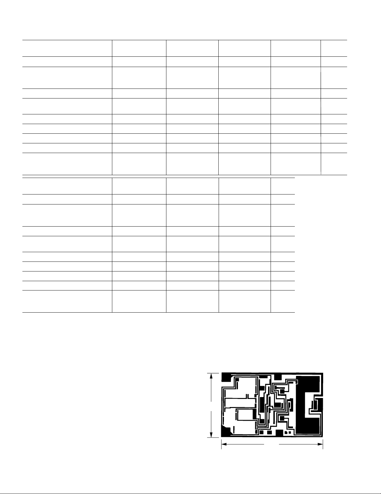
AD589 CHIP DIMENSIONS AND PAD LAYOUT
Current . . . . . . . . . . . . . . . . . . . . . . . . . . . . . . . . . . . . . 10 mA
Reverse Current . . . . . . . . . . . . . . . . . . . . . . . . . . . . . . . 10 mA
Power Dissipation
1
. . . . . . . . . . . . . . . . . . . . . . . . . . .125 mW
Storage Temperature . . . . . . . . . . . . . . . . . . .–65°C to +175°C
Operating Junction Temperature Range . . . .–55°C to +150°C
Lead Temperature (Soldering, 10 sec) . . . . . . . . . . . . . +300°C
NOTE
1
Absolute maximum power dissipation is limited by maximum current through the
device. Maximum rating at elevated temperatures must be computed assuming
TJ≤ 150°C, and θJA = 400 = C/W.
0.040
(1.016)
0.060
(1.524)
THE AD589 IS AVAILABLE IN CHIP FORM WITH FULLY TESTED
AND GUARANTEED SPECIFICATIONS. CONSULT FACTORY FOR
AVAILABLE GRADES AND PRICING.
–2–
REV. B
Page 3

Understanding the Specifications–AD589
R1 R5 R6
R2
R7 C1
Q2
R4
Q1
R3
Q3 Q4
–V
+V
Q5
Q8
Q7
Q9
VOLTAGE VARIATION VS. TEMPERATURE
Some confusion exists in the area of defining and specifying
reference voltage error over temperature. Historically, references
have been characterized using a maximum deviation per degree
Centigrade; i.e., 10 ppm/°C. However, because of nonlinearities
in temperature characteristics, which originated in standard
Zener references (such as “S” type characteristics) most
manufacturers have begun to use a maximum limit error band
approach to specify devices. This technique involves measurement of the output at 3, 5 or more different temperatures to
guarantee that the output voltage will fall within the given error
band. The temperature characteristics of the AD589 consistently follows the curve shown in Figure 1. Three-point
measurement guarantees the error band over the specified
temperature range. The temperature coefficients specified on
the previous page represent the slopes of the diagonals of the
error band from +25°C to T
1.2370
1.2365
1.2360
1.2355
OUTPUT VOLTAGE – V
1.2350
and +25°C to T
MIN
MAX
.
DYNAMIC PERFORMANCE
Many low power instrument manufacturers are becoming
increasingly concerned with the turn-on characteristics of the
components being used in their systems. Fast turn-on components often enable the end user to keep power off when not
needed, and yet respond quickly when the power is turned on
for operation. Figure 3 displays the turn-on characteristics of the
AD589. This characteristic is generated from cold-start operation and represents the true turn-on waveform after an extended
period with the supplies off. The figure shows both the coarse
and fine transient characteristics of the device; the total settling
time to within ±1 millivolt is about 25 µs, and there is no long
thermal tail appearing after that point.
200mV
100
90
10
0%
10mV
10µs
Figure 3. Output Settling Characteristics
1.2345
–50
–25
TEMPERATURE – °C
+125
+100+75+50+250
Figure 1. Typical AD589 Temperature Characteristics
1000
100
10
NOISE SPECTRAL DENSITY – nV/ Hz
0
10 100 1M100k10k1k
FREQUENCY – Hz
Figure 2. Noise Spectral Density
Figure 4. Schematic Diagram
REV.B
–3–
Page 4

AD589
AD589
6.2kΩ
10kΩ
1kΩ
+5V
+V
7107
REF HI
REF LO
COMMON
AD589
2 1 16
R
FB
OUT1OUT2
REF
GND
V
DD
+15V
R2
5kΩ
14
15
3
R1
39kΩ
–15V
V
OUT
=
0 TO 1.00V
MSB LSB
23456789
BIT
1
BIT
10
AD7533 SERIES
AD542L
APPLICATION INFORMATION
The AD589 functions as a two-terminal shunt-type regulator. It
provides a constant 1.23 V output for a wide range of input
current from 50 µA to 5 mA. Figure 5 shows the simplest
configuration for an output voltage of 1.2 V or less. Note that
no frequency compensation is required. If additional filtering is
desired for ultralow noise applications, minimum recommended
capacitance is 1000 pF.
+5V
6.8kΩ
AD589
Figure 5. Basic Configuration for 1.2 V or Less
The AD589 can also be used as a building block to generate
other values of reference voltage. Figure 6 shows a circuit which
produces a buffered 10 V output. Total supply current for this
circuit is approximately 2 mA.
AD589
10kΩ
V
OUT
b. With 7107 Panel Meter A/D
Figure 7. AD589 Used as Reference for CMOS
A/D Converters
The AD589 also is useful as a reference for CMOS multiplying
DACs such as the AD7533. These DACs require a negative
reference voltage in order to provide a positive output range.
Figure 8 shows the AD589 used to supply an equivalent –1.0 V
reference to an AD7533.
C547c–2–7/88
+15V
15kΩ
2
3
7
AD108A
4
1
0.01µF
6
8
1kΩ
1kΩ
8.2kΩ
10V
Figure 6. Single Supply Buffered 10 V Reference
The low power operation of the AD589 makes it ideal for use in
battery operated portable equipment. It is especially useful as a
reference for CMOS analog-to-digital converters. Figure 7
shows the AD589 used in conjunction with two popular
integrating type CMOS A/D converters.
+5V
5.6kΩ
+V
REF+
REF–
REF OUT
7109
AD589
a. With 7109 12-Bit Binary A/D
6.8kΩ
2kΩ
–4–
Figure 8. AD589 as Reference for 10-Bit CMOS DAC
OUTLINE DIMENSIONS AND PIN DESIGNATIONS
Dimensions shown in inches and (mm).
45°
0.036 (0.91)
0.046 (1.17)
0.10 (2.54)
0.195 (4.95)
0.178 (4.52)
0.028 (0.71)
0.048 (1.22)
DIA
0.015 (0.38)
0.019 (0.48)
0.209 (5.31)
0.230 (5.84)
0.500 (12.7)
MIN
DIA
0.150 (3.81)
0.125 (3.17)
REV. B
PRINTED IN U.S.A.
 Loading...