

Page 1
High Speed, Precision
a
FEATURES
3.0 ms Acquisition Time to 60.01% max
Low Droop Rate: 1.0 mV/ms max
Sample/Hold Offset Step: 3 mV max
Aperture Jitter: 0.5 ns
Extended Temperature Range: –558C to +1258C
Internal Hold Capacitor
Internal Application Resistors
612 V or 615 V Operation
Available in Surface Mount
APPLICATIONS
Data Acquisition Systems
Data Distribution Systems
Analog Delay & Storage
Peak Amplitude Measurements
MIL-STD-883 Compliant Versions Available
PRODUCT DESCRIPTION
The AD585 is a complete monolithic sample-and-hold circuit
consisting of a high performance operational amplifier in series
with an ultralow leakage analog switch and a FET input integrating amplifier. An internal holding capacitor and matched
applications resistors have been provided for high precision and
applications flexibility.
The performance of the AD585 makes it ideal for high speed
10- and 12-bit data acquisition systems, where fast acquisition
time, low sample-to-hold offset, and low droop are critical. The
AD585 can acquire a signal to ±0.01% in 3 µs maximum, and
then hold that signal with a maximum sample-to-hold offset of
3 mV and less than 1 mV/ms droop, using the on-chip hold
capacitor. If lower droop is required, it is possible to add a
larger external hold capacitor.
The high speed analog switch used in the AD585 exhibits
aperture jitter of 0.5 ns, enabling the device to sample full scale
(20 V peak-to-peak) signals at frequencies up to 78 kHz with
12-bit precision.
The AD585 can be used with any user-defined feedback network to provide any desired gain in the sample mode. On-chip
precision thin-film resistors can be used to provide gains of +1,
–1, or +2. Output impedance in the hold mode is sufficiently
low to maintain an accurate output signal even when driving the
dynamic load presented by a successive-approximation A/D
converter. However, the output is protected against damage
from accidental short circuits.
The control signal for the HOLD command can be either active
high or active low. The differential HOLD signal is compatible
with all logic families, if a suitable reference level is provided. An
on-chip TTL reference level is provided for TTL compatibility.
Sample-and-Hold Amplifier
AD585
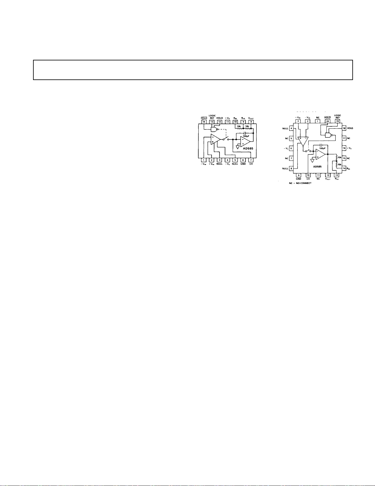
FUNCTIONAL BLOCK DIAGRAM
DIP LCC/PLCC Package
The AD585 is available in three performance grades. The JP
grade is specified for the 0°C to +70°C commercial temperature
range and packaged in a 20-pin PLCC. The AQ grade is specified for the –25°C to +85°C industrial temperature range and is
packaged in a 14-pin cerdip. The SQ and SE grades are specified for the –55°C to +125°C military temperature range and
are packaged in a 14-pin cerdip and 20-pin LCC.
PRODUCT HIGHLIGHTS
1. The fast acquisition time (3 µs) and low aperture jitter
(0.5 ns) make it the first choice for very high speed data
acquisition systems.
2. The droop rate is only 1.0 mV/ms so that it may be used in
slower high accuracy systems without the loss of accuracy.
3. The low charge transfer of the analog switch keeps sample-to
hold offset below 3 mV with the on-chip 100 pF hold capacitor, eliminating the trade-off between acquisition time and
S/H offset required with other SHAs.
4. The AD585 has internal pretrimmed application resistors for
applications versatility.
5. The AD585 is complete with an internal hold capacitor for
ease of use. Capacitance can be added externally to reduce
the droop rate when long hold times and high accuracy are
required.
6. The AD585 is recommended for use with 10- and 12-bit
successive-approximation A/D converters such as AD573,
AD574A, AD674A, AD7572 and AD7672.
7. The AD585 is available in versions compliant with MIL-STD-
883. Refer to the Analog Devices Military Products Databook
or current AD585/883B data sheet for detailed specifications.
REV. A
Information furnished by Analog Devices is believed to be accurate and
reliable. However, no responsibility is assumed by Analog Devices for its
use, nor for any infringements of patents or other rights of third parties
which may result from its use. No license is granted by implication or
otherwise under any patent or patent rights of Analog Devices.
One Technology Way, P.O. Box 9106, Norwood, MA 02062-9106, U.S.A.
Tel: 617/329-4700 Fax: 617/326-8703
Page 2
(typical @ +258C and VS = 612 V or 615 V, and CH = Internal, A = +1,
AD585–SPECIFICATIONS
Model AD585J AD585A AD585S
SAMPLE/HOLD CHARACTERISTICS
Acquisition Time, 10 V Step to 0.01% 333µs
20 V Step to 0.01% 5 5 5 µs
Aperture Time, 20 V p-p Input,
HOLD 0 V 353535ns
Aperture Jitter, 20 V p-p Input,
HOLD 0 V 0.5 0.5 0.5 ns
Settling Time, 20 V p-p Input,
HOLD 0 V, to 0.01% 0.5 0.5 0.5 µs
Droop Rate 111mV/ms
Droop Rate T
Charge Transfer 0.3 0.3 0.3 pC
MIN
to T
MAX
Sample-to-Hold Offset –3 3 –3 3 –3 3 mV
Feedthrough
20 V p-p, 10 kHz Input 0.5 0.5 0.5 mV
TRANSFER CHARACTERISTICS
1
Open Loop Gain
V
= 20 V p-p, RL = 2k 200,000 200,000 200,000 V/V
OUT
Application Resistor Mismatch 0.3 0.3 0.3 %
Common-Mode Rejection
VCM = ±10 V 80 80 80 dB
Small Signal Gain Bandwidth
V
= 100 mV p-p 2.0 2.0 2.0 MHz
OUT
Full Power Bandwidth
V
= 20 V p-p 160 160 160 kHz
OUT
Slew Rate
V
= 20 V p-p 10 10 10 V/µs
OUT
Output Resistance (Sample Mode)
I
= ±10 mA 0.05 0.05 0.05 Ω
OUT
Output Short Circuit Current 50 50 50 mA
Output Short Circuit Duration Indefinite Indefinite Indefinite
ANALOG INPUT CHARACTERISTICS
Offset Voltage 522mV
Offset Voltage, T
Bias Current 222nA
Bias Current, T
Input Capacitance, f = 1 MHz 10 10 10 pF
MIN
MIN
to T
to T
MAX
MAX
Input Resistance, Sample or Hold
20 V p-p Input, A = +1 10
DIGITAL INPUT CHARACTERISTICS
TTL Reference Output 1.2 1.4 1.6 1.2 1.4 1.6 1.2 1.4 1.6 V
Logic Input High Voltage
T
to T
MIN
MIN
to T
MAX
MAX
Logic Input Low Voltage
T
Logic Input Current (Either Input) 50 50 50 µA
POWER SUPPLY CHARACTERISTICS
Operating Voltage Range +5, –10.8 ±18 +5, –10.8 ±18 +5, –10.8 ± 18 V
Supply Current, RL = ∞ 610610610mA
Power Supply Rejection, Sample Mode 70 70 70 dB
TEMPERATURE RANGE
Specified Performance 0 +70 –25 +85 –55 +125 °C
PACKAGE OPTIONS
3, 4
Cerdip (Q-14) AD585AQ AD585SQ
LCC (E-20A) AD585SE
PLCC (P-20A) AD585JP
Min Typ Max Min Typ Max Min Typ Max Units
Doubles Every 10°C Double Every 10°C Doubles Every 10°C
2.0 2.0 2.0 V
HOLD active unless otherwise noted)
633mV
552050
12
0.8 0.8 0.7 V
10
12
10
12
2
nA
Ω
NOTES
1
Maximum input signal is the minimum supply minus a headroom voltage of 2.5 V.
2
Not tested at –55°C.
3
E = Leadless Ceramic Chip Carrier; P = Plastic Leaded Chip Carrier; Q = Cerdip.
4
For AD585/883B specifications, refer to Analog Devices Military Products Databook.
Specifications subject to change without notice.
Specifications shown in boldface are tested on all production units at final electrical
test. Results from those tests are used to calculate outgoing quality levels.
All min and max specifications are
guaranteed, although only those shown in
boldface are tested on all production units.
–2–
REV. A
Page 3

ABSOLUTE MAXIMUM RATINGS
Supplies (+VS, –V
) . . . . . . . . . . . . . . . . . . . . . . . . . . . . .±18 V
S
Logic Inputs . . . . . . . . . . . . . . . . . . . . . . . . . . . . . . . . . . . ±V
Analog Inputs . . . . . . . . . . . . . . . . . . . . . . . . . . . . . . . . . . ±V
RIN, R
Pins . . . . . . . . . . . . . . . . . . . . . . . . . . . . . . . . . . . ±V
FB
Storage Temperature . . . . . . . . . . . . . . . . . . . –65°C to +150°C
Lead Temperature (Soldering) . . . . . . . . . . . . . . . . . . . 300°C
Output Short Circuit to Ground . . . . . . . . . . . . . . . . Indefinite
TTL Logic Reference Short
Circuit to Ground . . . . . . . . . . . . . . . . . . . . . . . . . Indefinite
AD585
S
S
S
REV. A
Figure 2. Acquisition Time vs. Hold Capacitance
(10 V Step to 0.01%)
–3–
Page 4

AD585
SAMPLED DATA SYSTEMS
In sampled data systems there are a number of limiting factors
in digitizing high frequency signals accurately. Figure 9 shows
pictorially the sample-and-hold errors that are the limiting factors. In the following discussions of error sources the errors will
be divided into the following groups: 1. Sample-to-Hold Transition, 2. Hold Mode and 3. Hold-to-Sample Transition.
Figure 9. Pictorial Showing Various S/H Characteristics
SAMPLE-TO-HOLD TRANSITION
The aperture delay time is the time required for the sample-andhold amplifier to switch from sample to hold. Since this is effectively a constant then it may be tuned out. If however, the
aperture delay time is not accounted for then errors of the magnitude as shown in Figure 10 will result.
–(N + 1)
2
=
π(Aperture Jitter )
f
MAX
For an application with a 10-bit A/D converter with a 10 V full
scale to a 1/2 LSB error maximum.
–(10 +1)
2
=
π(0.5 ×10
= 310.8 kHz.
–9
)
f
MAX
f
MAX
For an application with a 12-bit A/D converter with a 10 V full
scale to a 1/2 LSB error maximum:
–(12 +1)
2
=
π(0.5 ×10
= 77.7 kHz.
–9
)
f
MAX
f
MAX
Figure 11 shows the entire range of errors induced by aperture
jitter with respect to the input signal frequency.
Figure 10. Aperture Delay Error vs. Frequency
To eliminate the aperture delay as an error source the sampleto-hold command may be advanced with respect to the input
signal .
Once the aperture delay time has been eliminated as an error
source then the aperture jitter which is the variation in aperture
delay time from sample-to-sample remains. The aperture jitter is
a true error source and must be considered. The aperture jitter
is a result of noise within the switching network which modulates the phase of the hold command and is manifested in the
variations in the value of the analog input that has been held.
The aperture error which results from this jitter is directly related to the dV/dT of the analog input.
The error due to aperture jitter is easily calculated as shown below. The error calculation takes into account the desired accuracy corresponding to the resolution of the N-bit A/D converter.
–4–
Figure 11. Aperture Jitter Error vs. Frequency
Sample-to-hold offset is caused by the transfer of charge to the
holding capacitor via the gate capacitance of the switch when
switching into hold. Since the gate capacitance couples the
switch control voltage applied to the gate on to the hold capacitor, the resulting sample-to-hold offset is a function of the logic
level .
The logic inputs were designed for application flexibility and,
therefore, a wide range of logic thresholds. This was achieved by
using a differential input stage for HOLD and
HOLD. Figure 1
shows the change in the sample-to-hold offset voltage based
upon an independently programmed reference voltage. Since
the input stage is a differential configuration, the offset voltage
is a function of the control voltage range around the programmed threshold voltage.
The sample-to-hold offset can be reduced by adding capacitance
to the internal 100 pF capacitor and by using
HOLD instead of
HOLD. This may be easily accomplished by adding an external
capacitor between Pins 7 and 8. The sample-to-hold offset is
then governed by the relationship:
S/H Offset (V )=
Charge pC
CHTotal ( pF )
()
REV. A
Page 5

AD585
For the AD585 in particular it becomes:
S/H Offset (V )=
0.3 pC
100 pF + C
()
EXT
The addition of an external hold capacitor also affects the acquisition time of the AD585. The change in acquisition time with
respect to the C
HOLD MODE
is shown graphically in Figure 2.
EXT
In the hold mode there are two important specifications that
must be considered; feedthrough and the droop rate. Feedthrough
errors appear as an attenuated version of the input at the output
while in the hold mode. Hold-Mode feedthrough varies with frequency, increasing at higher frequencies. Feedthrough is an important specification when a sample and hold follows an analog
multiplexer that switches among many different channels.
Hold-mode droop rate is the change in output voltage per unit
of time while in the hold mode. Hold-mode droop originates as
leakage from the hold capacitor, of which the major leakage
current contributors are switch leakage current and bias current.
The rate of voltage change on the capacitor dV/dT is the ratio of
the total leakage current I
Droop Rate =
to the hold capacitance CH.
L
dV
OUT
dT
(Volts/Sec) =
I
C
L
H
( pA)
( pF )
For the AD585 in particular;
HOLD-TO-SAMPLE TRANSITION
The Nyquist theorem states that a band-limited signal which is
sampled at a rate at least twice the maximum signal frequency
can be reconstructed without loss of information. This means
that a sampled data system must sample, convert and acquire
the next point at a rate at least twice the signal frequency. Thus
the maximum input frequency is equal to
f
MAX
Where T
amplifier, T
is the acquisition time of the sample-to-hold
ACQ
is the maximum aperture time (small enough to
AP
be ignored) and T
=
2 T
()
ACQ+TCONV+TAP
is the conversion time of the A/D
CONV
1
converter.
DATA ACQUISITION SYSTEMS
The fast acquisition time of the AD585 when used with a high
speed A/D converter allows accurate digitization of high frequency signals and high throughput rates in multichannel data
acquisition systems. The AD585 can be used with a number of
different A/D converters to achieve high throughput rates. Figures 12 and 13 show the use of an AD585 with the AD578 and
AD574A.
Droop Rate =
100 pA
100 pF +(C
EXT
)
Additionally the leakage current doubles for every 10°C increase
in temperature above 25°C; therefore, the hold-mode droop rate
characteristic will also double in the same fashion. The hold-mode
droop rate can be traded-off with acquisition time to provide the
best combination of droop error and acquisition time. The tradeoff
is easily accomplished by varying the value of C
EXT
.
Since a sample and hold is used typically in combination with
an A/D converter, then the total droop in the output voltage has
to be less than 1/2 LSB during the period of a conversion. The
maximum allowable signal change on the input of an A/D
converter is:
∆V max =
Full -Scale Voltage
N +1
()
2
Once the maximum ∆V is determined then the conversion time
of the A/D converter (T
) is required to calculate the maxi-
CONV
mum allowable dV/dT.
dV
dt
The maximum
the limit not only at 25°C but at the maximum expected operat-
dV max
dT
as shown by the previous equation is
max =
∆V max
T
CONV
ing temperature range. Therefore, over the operating temperature
range the following criteria must be met (T
OPERATION
–25°C)
= ∆T.
∆T °C
()
dV 25°C
dT
× 2
10°C
dV max
≤
dT
Figure 12. A/D Conversion System, 117.6 kHz Throughput
58.8 kHz max Signal Input
Figure 13. 12-Bit A/D Conversion System, 26.3 kHz
Throughput Rate, 13.1 kHz max Signal Input
REV. A
–5–
Page 6

AD585
LOGIC INPUT
The sample-and-hold logic control was designed for versatile
logic interfacing. The HOLD and
HOLD inputs may be used
with both low and high level CMOS, TTL and ECL logic systems. Logic threshold programmability was achieved by using a
differential amplifier as the input stage for the digital inputs. A
predictable logic threshold may be programmed by referencing
either HOLD or
For example, if the internal 1.4 V reference is applied to
an input signal to HOLD between +1.8 V and +V
HOLD to the appropriate threshold voltage.
HOLD
will place
S
the AD585 in the hold mode. The AD585 will go into the
sample mode for this case when the input is between –V
and
S
+1.0 V. The range of references which may be applied is from
(–V
+4 V) to (+VS –3 V).
S
OPTIONAL CAPACITOR SELECTION
If an additional capacitor is going to be used in conjunction
with the internal 100 pF capacitor it must have a low dielectric
absorption. Dielectric absorption is just that; it is the charge
absorbed into the dielectric that is not immediately added to or
removed from the capacitor when rapidly charged or discharged.
The capacitor with dielectric absorption is modeled in Figure 14.
ence between the voltage being measured and the voltage previously measured determines the fraction by which the
dielectric absorption figure is multiplied. It is impossible to
readily correct for this error source. The only solution is to use a
capacitor with dielectric absorption less than the maximum
tolerable error. Capacitor types such as polystyrene, polypropylene or Teflon are recommended.
GROUNDING
Many data-acquisition components have two or more ground
pins which are not connected together within the device. These
“grounds” are usually referred to as the Logic Power Return
Analog Common (Analog Power Return), and Analog Signal
Ground. These grounds must be tied together at one point,
usually at the system power-supply ground. Ideally, a single
solid ground would be desirable. However, since current flows
through the ground wires and etch stripes of the circuit cards,
and since these paths have resistance and inductance, hundreds
of millivolts can be generated between the system ground point
and the ground pin of the AD585. Separate ground returns
should be provided to minimize the current flow in the path
from sensitive points to the system ground point. In this way
supply currents and logic-gate return currents are not summed
into the same return path as analog signals where they would
cause measurement errors.
C851c–5–4/89
Figure 14. Capacitor Model with Dielectric Absorption
If the capacitor is charged slowly, CDA will eventually charge to
the same value as C. But unfortunately, good dielectrics have
very high resistances, so while C
the time constant R
typically runs into the millisecond
X CDA
may be small, RX is large and
DA
range. In fast charge, fast-discharge situations the effect of dielectric absorption resembles “memory”. In a data acquisition
system where many channels with widely varying data are being
sampled the effect is to have an ever changing offset which appears as a very nonlinear sample-to-hold offset since the differ-
OUTLINE DIMENSIONS
Dimensions shown in inches and (mm).
14-Pin Cerdip (Q-14)
20-Terminal LCC (E-20A)
Figure 15. Basic Grounding Practice
20-Terminal PLCC (P-20A)
PRINTED IN U.S.A.
–6–
REV. A
 Loading...