

Page 1
High Precision,
FEATURES
Laser-trimmed to high accuracy: 2.500 V ±0.4%
3-terminal device: voltage in/voltage out
Excellent temperature stability: 10 ppm/°C (AD580M, U)
Excellent long-term stability: 250 µV (25 µV/month)
Low quiescent current: 1.5 mA maximum
Small, hermetic IC package: TO-52 can
MIL-STD-883 compliant versions available
GENERAL DESCRIPTION
The AD5801 is a 3-terminal, low cost, temperaturecompensated, bandgap voltage reference, which provides a fixed
2.5 V output for inputs between 4.5 V and 30 V. A unique
combination of advanced circuit design and laser-wafer
trimmed thin film resistors provide the AD580 with an initial
tolerance of ±0.4%, a temperature stability of better than 10
ppm/°C, and long-term stability of better than 250 µV. In
addition, the low quiescent current drain of 1.5 mA maximum
offers a clear advantage over classical Zener techniques.
The AD580 is recommended as a stable reference for all 8-, 10-,
and 12-bit D/A converters that require an external reference. In
addition, the wide input range of the AD580 allows operation
with 5 volt logic supplies, making the AD580 ideal for digital
panel meter applications or whenever only a single logic power
supply is available.
The AD580J, K, L, and M are specified for operation over the
0°C to +70°C temperature range; the AD580S, T, and U are
specified for operation over the extended temperature range of
–55°C to +125°C.
2.5 V IC Reference
AD580
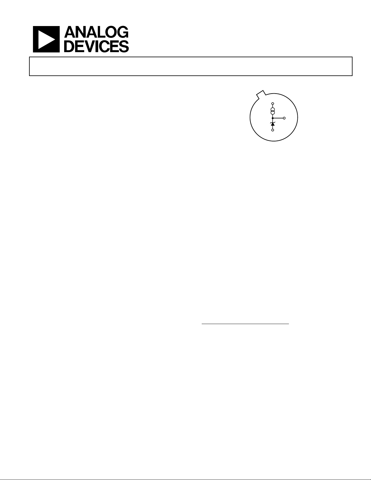
FUNCTIONAL BLOCK DIAGRAM
+E
E
–E
Figure 1.
OUT
00525-B-001
BOTTOM
VIEW
PRODUCT HIGHLIGHTS
1. Laser-trimming of the thin film resistors minimizes the
AD580 output error. For example, the AD580L output
tolerance is ±10 mV.
2. The three-terminal voltage in/voltage out operation of the
AD580 provides regulated output voltage without any
external components.
3. The AD580 provides a stable 2.5 V output voltage for input
voltages between 4.5 V and 30 V. The capability to provide
a stable output voltage using a 5 V input makes the AD580
an ideal choice for systems that contain a single logic
power supply.
4. Thin film resistor technology and tightly controlled bipolar
processing provide the AD580 with temperature stabilities
to 10 ppm/°C and long-term stability better than 250 µV.
5. The low quiescent current drain of the AD580 makes it
ideal for CMOS and other low power applications.
6. The AD580 is available in versions compliant with MIL-
STD-883. Refer to the Analog Devices Military Products
Data Book or the current AD580/AD883B data sheet for
detailed specifications.
1
Protected by U.S. Patent Numbers 3,887,863; RE30,586.
Rev. B
Information furnished by Analog Devices is believed to be accurate and reliable.
However, no responsibility is assumed by Analog Devices for its use, nor for any
infringements of patents or other rights of third parties that may result from its use.
Specifications subject to change without notice. No license is granted by implication
or otherwise under any patent or patent rights of Analog Devices. Trademarks and
registered trademarks are the property of their respective owners.
One Technology Way, P.O. Box 9106, Norwood, MA 02062-9106, U.S.A.
Tel: 781.329.4700
Fax: 781.326.8703 © 2004 Analog Devices, Inc. All rights reserved.
www.analog.com
Page 2

AD580
TABLE OF CONTENTS
Specifications..................................................................................... 3
The AD580 as a Current Limiter.................................................6
Absolute Maximum Ratings............................................................ 4
AD580 Chip Dimensions And Pad Layout............................... 4
ESD Caution.................................................................................. 4
Theory of Operation ........................................................................ 5
Voltage Variation versus Temperature ....................................... 5
Noise Performance ....................................................................... 6
REVISION HISTORY
8/04—Changed from Rev. A to Rev. B
Updated Format................................................................ Universal
The AD580 as a Low Power, Low Voltage, Precision Reference
for Data Converters
Outline Dimensions..........................................................................8
Ordering Guide .............................................................................8
.......................................................................7
Rev. B | Page 2 of 8
Page 3
AD580
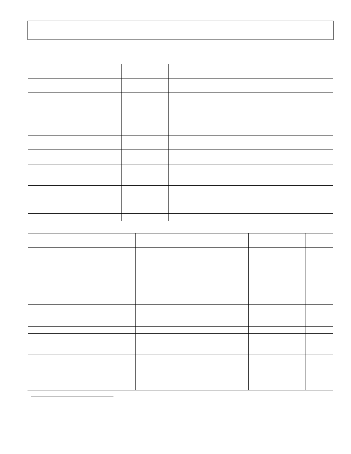
SPECIFICATIONS
Table 1. VIN = 15 V and 25°C
AD580J AD580K AD580L AD580M
Model Min Typ Max Min Typ Max Min Typ Max Min Typ Max Units
OUTPUT VOLTAGE TOLERANCE
Error from Nominal 2.500 V Output ±75 ±25 ±10 ±10 mV
OUTPUT VOLTAGE CHANGE
T
to T
MIN
85 40 25 10 ppm/°C
LINE REGULATION
7 V ≤ VIN ≤ 30 V 1.5
4.5 V ≤ VIN ≤ 7 V 0.3
LOAD REGULATION
∆I = 10 mA
QUIESCENT CURRENT 1.0
NOISE (0.1 Hz to 10 Hz) 8 8 8 8 µV p-p
STABILITY
Long Term 250 250 250 250 µV
Per Month 25 25 25 25 µV
TEMPERATURE PERFORMANCE
Specified 0 +70 0 +70 0 +70 0 +70 °C
Operating –55 +125 –55 +125 –55 +125 –55 +125 °C
Storage –65 +175 –65 +175 –65 +175 –65 +175 °C
PACKAGE OPTION2 TO-52 (H-03A) AD580JH AD580KH AD580LH AD580MH
Table 2.
AD580S AD580T AD580U
Model Min Typ Max Min Typ Max Min Typ Max Units
OUTPUT VOLTAGE TOLERANCE
Error from Nominal 2.500 V Output
OUTPUT VOLTAGE CHANGE
T
MIN
55 25 10 ppm/°C
LINE REGULATION
7 V ≤ VIN ≤ 30 V 1.5
4.5 V ≤ VIN ≤ 7 V 0.3
LOAD REGULATION
∆I = 10 mA
QUIESCENT CURRENT 1.0
NOISE (0.1 Hz to 10 Hz) 8 8 8 µV p-p
STABILITY
Long Term 250 250 250 µV
Per Month 25 25 25 µV
TEMPERATURE PERFORMANCE
Specified –55 +125 –55 +125 –55 +125 °C
Operating –55 +150 –55 +150 –55 +150 °C
Storage –65 +175 –65 +175 –65 +175 °C
PACKAGE OPTION2 TO-52 (H-03A) AD580SH AD580TH AD580UH
1
Specifications shown in boldface are tested on all production units at final electrical test. Results from those tests are used to calculate outgoing quality levels. All min
and max specifications are guaranteed, although only those shown in boldface are tested on all production units.
2
H = Metal Can.
15 7 4.3 1.75 mV
MAX
1
to T
MAX
6
3
10
1.5
1.5 4
0.3 2
1.0
1
±25
25
6
3
10
1.5
10
1.5
1.0
1.0
±10
11
2
1
10
1.5
2
1
10
1.5
1.0
1.0
±10
4.5
2
1
10
1.5
2
1
10
1.5
mV
mV
mV
mA
mV
mV
mV
mV
mV
mA
Rev. B | Page 3 of 8
Page 4

AD580
ABSOLUTE MAXIMUM RATINGS
Table 3.
Parameter Rating
Input Voltage 40 V
Power Dissipation @ 25°C
Ambient Temperature 350 mW
Derate above 25°C 2.8 mW/°C
Lead Temperature (Soldering
10 sec)
Thermal Resistance
Junction-to-Case 100°C
Junction-to-Ambient 360°C/W
Stresses above those listed under Absolute Maximum Ratings
may cause permanent damage to the device. This is a stress
rating only; functional operation of the device at these or any
other conditions above those listed in the operational sections
of this specification is not implied. Exposure to absolute
maximum rating conditions for extended periods may affect
device reliability.
300°C
AD580 CHIP DIMENSIONS AND PAD LAYOUT
Dimensions shown in inches and (millimeters).
0.075 (1.90)
+E
0.046
(1.16)
*BOTH E
PADS MUST BE CONNECTED TO THE OUTPUT.
OUT
Figure 2.
*
E
OUT
The AD580 is also available in chip form. Consult the factory
for specifications and applications information.
–E
00525-B-002
ESD CAUTION
ESD (electrostatic discharge) sensitive device. Electrostatic charges as high as 4000 V readily accumulate on
the human body and test equipment and can discharge without detection. Although this product features
proprietary ESD protection circuitry, permanent damage may occur on devices subjected to high energy
electrostatic discharges. Therefore, proper ESD precautions are recommended to avoid performance
degradation or loss of functionality.
Rev. B | Page 4 of 8
Page 5

AD580
THEORY OF OPERATION
The AD580 family (AD580, AD581, AD584, AD589) uses the
bandgap concept to produce a stable, low temperature coefficient voltage reference suitable for high accuracy data acquisition components and systems. The device makes use of the
underlying physical nature of a silicon transistor base-emitter
voltage in the forward-biased operating region. All such transistors have approximately a –2 mV/°C temperature coefficient,
unsuitable for use directly as a low TC reference. Extrapolation
of the temperature characteristic of any one of these devices to
absolute zero (with an emitter current propor-tional to the
absolute temperature), however, reveals that it will go to a V
1.205 V at 0 K, as shown in Figure 3. Thus, if a voltage could be
developed with an opposing temperature coefficient to sum
with V
to total 1.205 V, a 0 TC reference would result and
BE
operation from a single, low voltage supply would be possible.
The AD580 circuit provides such a compensating voltage, V1 in
Figure 4, by driving two transistors at different current densities
and amplifying the resulting V
has a positive TC). The sum, V
difference (∆VBE—which now
BE
, is then buffered and amplified
Z
up to 2.5 V to provide a usable reference-voltage output. Figure
5 shows the schematic diagram of the AD580.
The AD580 operates as a 3-terminal reference, meaning that no
additional components are required for biasing or current
setting. The connection diagram, Figure 6, is quite simple.
1.5
CONSTANT SUM = 1.205V
1.205
1.0
FOR BOTH
DEVICES
of
BE
+V
IN
∆
V
BE
2I1= I1+ I
COM
Q28AQ1
2
R7R8
I
≅
I
2
1
A
R2
VBE (Q1)
R
1
V1= 2
R1
∆
R
2
V
OUT
R4
= VBE + V
V
Z
R5
V
BE
= VBE + 2
= VBE + 2 ln
= 1.205V
Figure 4. Basic Bandgap-Reference Regulator Circuit
COM
R8
Q10 Q11
Q8
R3
Q2
8A
R2
R1
+E
Q9
Q3
R7
Q1
A
R6
Q14
Q12
C1
R12 R13
Q13
Q15
R11
Figure 5. Schem atic Diag ram
+E
≤
V
≤
4.5
30V
IN
R
= VZ 1 + = 2.5V
Q5
4
R
5
1
R
1
∆
V
BE
R
2
kTqJ
R
1
R
2
Q4
Q7
Q6
R9
R10
R4
R5
–E
1
J
2
00525-B-004
2.5V
OUT
00525-B-005
V
VS. TEMPERATURE
BE
FOR TWO TYPICAL
0.5
JUNCTION VOLTAGE (V)
0
–273°C –200°C –100°C 100°C0°C
DEVICES (I
0K 73K 173K 373K273K
α
T)
E
TEMPERATURE
REQUIRED
COMPENSATION
VOLTAGE–
SAME DEVICES
Figure 3. Extrapolated Variation of Base-Emitter Voltage with Temperature
αT), and Required Compensation, Shown for Two Different Devices
(I
E
00525-B-003
Rev. B | Page 5 of 8
E
AD580
Figure 6. Connection Diagram
OUT
LOAD
–E
00525-B-006
VOLTAGE VARIATION VERSUS TEMPERATURE
Some confusion exists in the area of defining and specifying
reference voltage error over temperature. Historically, references
are characterized using a maximum deviation per degree
Centigrade; i.e., 10 ppm/°C. However, because of the
inconsistent nonlinearities in Zener references (butterfly or S
type characteristics), most manufacturers use a maximum limit
error band approach to characterize their references. This
technique measures the output voltage at 3 to 5 different
temperatures and guarantees that the output voltage deviation
will fall within the guaranteed error band at these discrete
temperatures. This approach, of course, makes no mention or
guarantee of performance at any other temperature within the
operating temperature range of the device.
Page 6

AD580
V
V
x
The consistent voltage versus temperature performance of a
typical AD580 is shown in Figure 7. Note that the characteristic
is quasi-parabolic, not the possible S type characteristics of
classical Zener references. This parabolic characteristic permits
a maximum output deviation specification over the device’s full
operating temperature range, rather than just at 3 to 5 discrete
temperatures.
2.51
2.50
2.49
2.48
OUTPUT VOLTAGE (V)
2.47
2.46
–55 –30 0 25 50 75 100 125
Figure 7. Typical AD580K Output Voltage vs. Temperature
MAXIMUM
VOLTAGE CHANGE
FROM 0°C TO 70°C
TEMPERATURE (°C)
00525-B-007
The AD580M guarantees a maximum deviation of 1.75 mV
over the 0°C to 70°C temperature range. This can be shown to
be equivalent to 10 ppm/°C average maximum; i.e.,
75.1
m
70
ma
°
C
1
5.2
°=×
averageCppm
max/10
The AD580 typically exhibits a variation of 1.5 mV over the
power supply range of 7 V to 30 V. Figure 8 is a plot of AD580
line rejection versus frequency.
NOISE PERFORMANCE
Figure 9 represents the peak-to-peak noise of the AD580 from
1 Hz (3 dB point) to a 3 dB high end shown on the horizontal
axis. Peak-to-peak noise from 1 Hz to 1 MHz is approximately
600 µV.
140
130
120
110
100
90
80
70
, p-p (mV)
60
OUT
E
50
40
30
20
10
0
10 100 1k 10k 100k
e = 23V p-p
E = 18.5V
E IN COMPOSITE (17V
Figure 8. AD580 Line Rejection Plot
AD580
≤
V
≤
IN
LINE FREQUENCY (Hz)
k e OUT p-p
30V)
00525-B-008
1mV
100µV
10µV
PEAK-TO-PEAK NOISE
0
100 1k 10k 100k 1M
FREQUENCY (Hz)
Figure 9. Peak-to-Peak Output Noise vs. Frequency
00525-B-009
500µA
5V
Figure 10. Input Current vs. Input Voltage (Integral Loads)
00525-B-010
THE AD580 AS A CURRENT LIMITER
The AD580 represents an excellent alternative to current limiter
diodes that require factory selection to achieve a desired
current. This approach often results in temperature coefficients
of 1%/C. The AD580 approach is not limited to a specially
selected factory set current limit; it can be programmed from
1 mA to 10 mA with the insertion of a single external resistor.
The approximate temperature coefficient of current limit for the
2.5V
R
LOAD
= 1 mA and
LIM
2.5V
i
≅
R
+ 1mA
00525-B-011
AD580 used in this mode is 0.13%/°C for I
0.01%/°C for I
= 13 mA (see Figure 11). Figure 10 displays
LIM
the high output impedance of the AD580 used as a current
limiter for I
BOTTOM VIEW OF
2.5V PRECISION
REFERENCE CIRCUIT
IN TO-52 CASE
= 1, 2, 3, 4, and 5 mA.
LIM
V+
AD580
OUTPUT
V–
Figure 11. A Two-Component Precision Current Limiter
Rev. B | Page 6 of 8
Page 7

AD580
THE AD580 AS A LOW POWER, LOW VOLTAGE,
PRECISION REFERENCE FOR DATA CONVERTERS
The AD580 has a number of features that make it ideally suited
for use with A/D and D/A data converters used in complex
microprocessor-based systems. The calibrated 2.500 V output
minimizes user trim requirements and allows operation from a
single, low voltage supply. Low power consumption (1 mA
quiescent current) is commensurate with that of CMOS-type
devices, while the low cost and small package complements the
decreasing cost and size of the latest converters.
Figure 12 shows the AD580 used as a reference for the AD7542
12-bit CMOS DAC with complete microprocessor interface.
The AD580 and the AD7542 are specified to operate from a
single 5 V supply, thus eliminating the need to provide a 15 V
power supply for the sole purpose of operating a reference. The
AD7542 includes three 4-bit data registers, a 12-bit DAC
register, and address decoding logic. It may thus be interfaced
directly to a 4-, 8- or 16-bit data bus. Only 8 mA of quiescent
current from the single 5 volt supply is required to operate the
AD7542 which is packaged in a small, 16-pin DIP. The AD544
output amplifier is also low power, requiring only 2.5 mA
quiescent current. Its laser-trimmed offset voltage preserves the
±1/2 LSB linearity of the AD7542KN without user trims, and it
typically settles to ±1/2 LSB in less than 3 µs. It will provide the
0 V to –2.5 V output swing from ±5 V supplies.
+5V
+E
E
OUT
AD580
SYSTEM
8-BIT DATA BUS
AD7 AD0
FROM SYSTEM RESET
FROM ADDRESS BUS
FROM ADDRESS DECODER
FROM WR
A0
A1
V
DD
D0
7
D1
6
D2
D3
CLR
AD7542
5
4
13
10
11
A0
A1
WR
Figure 12. Low Power, Low Voltage Reference for the AD7542
Microprocessor-Compatible, 12-Bit DAC
GAIN
–E
500Ω
ADJUST
V
REF
1514
9
812
CS
DGND
200Ω
RFB
16
1
2
3
AGND
I
OUT1
I
OUT2
22pF
AD544L
–5V
ANALOG
INPUT
00525-B-012
Rev. B | Page 7 of 8
Page 8

AD580
OUTLINE DIMENSIONS
ORDERING GUIDE
Output Voltage
Model
To le ra n ce
0.500 (12.70)
0.150 (3.81)
0.115 (2.92)
0.195 (4.95)
0.178 (4.52)
0.230 (5.84)
0.209 (5.31)
0.030 (0.76) MAX
CONTROLLING DIMENSIONS ARE IN INCHES; MILLIMETERS DIMENSIONS
(IN PARENTHESES) ARE ROUNDED-OFF INCH EQUIVALENTS FOR
REFERENCE ONLY AND ARE NOT APPROPRIATE FOR USE IN DESIGN
MIN
0.250 (6.35) MIN
0.050 (1.27) MAX
0.019 (0.48)
0.016 (0.41)
0.021 (0.53) MAX
BASE & SEATING PLANE
0.100
(2.54)
T.P.
0.050 (1.27) T.P.
3
2
1
0.050
(1.27)
T.P.
45° T.P.
Figure 13. TO–52 Package
Dimensions shown in inches and (millimeters)
Temperature
Coefficient
Operating
Temperature Range Package Option
0.048 (1.22)
0.028 (0.71)
0.046 (1.17)
0.036 (0.91)
Package
Description
AD580JH ±75 mV 85 ppm/°C –55°C to +125°C TO–52 H (Metal Can)
AD580KH ±25 mV 40 ppm/°C –55°C to +125°C TO–52 H (Metal Can)
AD580LH ±10 mV 25 ppm/°C –55°C to +125°C TO–52 H (Metal Can)
AD580LMH ±10 mV 10 ppm/°C –55°C to +125°C TO–52 H (Metal Can)
AD580SH ±25 mV 55 ppm/°C –55°C to +125°C TO–52 H (Metal Can)
AD580SH/883B ±25 mV 55 ppm/°C –55°C to +125°C TO–52 H (Metal Can)
AD580TH ±10 mV 25 ppm/°C –55°C to +125°C TO–52 H (Metal Can)
AD580UH ±10 mV 10 ppm/°C –55°C to +125°C TO–52 H (Metal Can)
AD580UH/883B ±10 mV 10 ppm/°C –55°C to +125°C TO–52 H (Metal Can)
AD580TCHIPS ±10 mV DIE
© 2004 Analog Devices, Inc. All rights reserved. Trademarks and
registered trademarks are the property of their respective owners.
C00525-0-8/04(B)
Rev. B | Page 8 of 8
 Loading...