

Page 1
Industrial I/V Output Driver,
Single Supply, 60v Compliance,
Programmable Ranges
Preliminary Technical Data
FEATURES
Current Output Ranges: 4–20mA, 0–20mA or 0–24mA,
0.1% Total Unadjusted Error (TUE)
5ppm/°C Output Drift
60V MAX IOUT Compliance Voltage
Voltage Output Ranges: 0-5V, 0-10V, 0-40v
20% over-range
0.1% Total Unadjusted Error (TUE)
Flexible Serial Digital Interface
On-Chip Output Fault Detection
PEC Error Checking
Asynchronous CLEAR Function
Power Supply Range
AV
: = +12V to +60V (MAX)
DD
Output Loop Compliance to AV
Temperature Range: -40°C to +105°C
LFCSP Packages
APPLICATIONS
Process Control
Actuator Control
PLC
GENERAL DESCRIPTION
The AD5751 is a single channel, low-cost, precision,
voltage/current output driver with hardware or software
programmable output ranges. The software ranges are
configured via an SPI/Microwire compatible serial interface.
The AD5751 targets applications in PLC and industrial process
control. The analog input to the AD5751 is provided from a
low voltage, single supply digital-to-analog converter and is
internally conditioned to provide the desired output
current/voltage range.
The output current range is programmable across three current
ranges - 4–20mA, 0–20mA or 0–24mA.
– 2.5 V
DD
AD5751
Voltage output is provided from a separate pin that can be
configured to provide 0V to 5V, 0V to 10V and 0-40V output
ranges. An over-range of 10% is available on the voltage
ranges.
Analog outputs are short and open circuit protected and can
drive capacitive loads of 1uF and inductive loads of 0.1H.
The device is specified to operate with a power supply range
from 12 V to 60 V. Output loop compliance is 0 V to AV
2.5 V.
The flexible serial interface is SPI
and MICROWIRE
compatible and can be operated in 3-wire mode to minimize the
digital isolation required in isolated applications. The interface
also features an optional PEC error checking feature using
CRC-8 error checking, useful in industrial environments where
data communication corruption can occur.
The device also includes a power-on-reset function ensuring
that the device powers up in a known state and an
asynchronous CLEAR pin which sets the outputs to zero-scale /
mid-scale voltage output or the low end of the selected current
range.
A HW SELECT pin is used to configure the part for hardware
or software mode on power up.
The total output error is typically ±0.1% in both current mode
and voltage mode.
Table 1. Related Devices
Part Number Description
AD5422
Single Channel, 16-Bit, Serial
Input Current Source and
Voltage Output DAC
DD
–
Rev. PrA
Information furnished by Analog Devices is believed to be accurate and reliable. However, no
responsibility is assumed by Analog Devices for its use, nor for any infringements of patents or other
rights of third parties that may result from its use. Specifications subject to change without notice. No
license is granted by implication or otherwise under any patent or patent rights of Analog Devices.
Trademarks and registered trademarks are the property of their respective owners.
One Technology Way, P.O. Box 9106, Norwood, MA 02062-9106, U.S.A.
Tel: 781.329.4700 www.analog.com
Fax: 781.461.3113 ©2008 Analog Devices, Inc. All rights reserved.
Page 2

AD5751 Preliminary Technical Data
TABLE OF CONTENTS
Features .............................................................................................. 1
Applications ....................................................................................... 1
General Description ......................................................................... 1
Revision History ............................................................................... 2
Functional Block Diagram .............................................................. 3
Specifications ..................................................................................... 4
Timing Characteristics ................................................................ 6
Absolute Maximum Ratings ............................................................ 9
ESD Caution .................................................................................. 9
Pin Configuration and Function Descriptions ........................... 10
Typical Performance Characteristics ........................................... 12
Terminology ................................. Error! Bookmark not defined.
Theory of Operation ................... Error! Bookmark not defined.
CURRENT OUTPUT Architecture ......................................... 14
OUTEN ........................................................................................ 14
Software control:......................................................................... 15
HARDWARE CONTROL: ........................................................ 17
Features ............................................................................................ 19
output fault alert – SOFTWARE MODE ................................ 19
output fault alert – HARDWARE MODE ............................... 19
voltage output short circuit protection .................................... 19
Asynchronous Clear (CLEAR) ................................................. 19
External current setting resistor ............................................... 20
Applications Information .............................................................. 21
Transient voltage protection ..................................................... 21
Layout Guidelines....................................................................... 21
Galvanically Isolated Interface ................................................. 21
Microprocessor Interfacing ....................................................... 21
Outline Dimensions ....................................................................... 22
Ordering Guide .......................................................................... 22
REVISION HISTORY
PrA – Preliminary Version. May 6, 2008
Rev. PrA | Page 2 of 22
Page 3
Preliminary Technical Data AD5751
FUNCTIONAL BLOCK DIAGRAM
CLEAR
CLRSEL
SCLK/OUTEN*
SDIN/R0*
SYNC/RSEL*
SDO/VFAULT*
HW SELECT
VIN
VREF
RESET
FAULT/TEMP*
NC/IFAULT*
INPUT SHIFT
REGISTER
AND
CONTROL
LOGIC
STATUS REG
OVERTEMP
VOUT SHORT F A ULT
IOUT OPEN FAULT
OUTPUT RANG E ERROR
AD5751
DVCC
VOUT RANGE
SCALING
IOUT RANGE
SCALING
POWER
RESET
ON
GND
AVDD
GND
R2
R1
COMP2COMP1
VSENSE+
VOUT
VOUT SHORT FAULT
AVDD
R3
IOUT
RSET
IOUT OPEN FAULT
AD2/R1*
AD1/R2*
AD0/R3*
Figure 1. Functional Block Diagram
* Denotes shared pin. Software mode denoted by regular text, hardware mode denoted by bold
text. E.G. for FAULT/TEMP pin, in software mode this pin will take on FAULT function. In
Hardware mode, this pin will take on TEMP function.
Rev. PrA | Page 3 of 22
Page 4
AD5751 Preliminary Technical Data
SPECIFICATIONS
AVDD=12V (+/-10%) to +60V (MAX) , DVCC =2.7 V to 5.5 V, GND = 0 V. RL = 2 kΩ, CL = 200 pF, IOUT : RL = 300Ω, HL =
50mH All specifications T
MIN
to T
Table 2.
Parameter Value
INPUT VOLTAGE RANGE
Input Leakage Current 1 uA max
VOLTAGE OUTPUT
Output Voltage Ranges 0 to 5 V
0 to 10 V
0 to 40 V
ACCURACY Output unloaded
Unipolar Output
Total Unadjusted Error (TUE) 0.1 % FSR max Over temperature and supplies.
Relative Accuracy (INL) ±0.02 % FSR max
Offset Error 0.015 % FSR max Error at analog input = 100mv (?)
Zero Scale Error TBD % FSR max Error at analog input = 0.0v
Zero Scale TC TBD ppm % FSR max
Gain Error 0.005 % FSR max (Ideal Span – Measured Span)/Ideal Span
Gain Error TC TBD ppm % FSR max
Full Scale Error 0.015 % FSR max Error at analog input = 4.096v (FS)
Full Scale Error TC TBD ppm % FSR max
Short-Circuit Current 15 mA max
Load Conditions
Resistance 1 K Ohm min For Specified Performance, 0-5v, 0-10v ranges.
Resistance 5 K Ohm min For Specified Performance, 0-40v ranges.
Capacitance Load Stability
RL = ∞ 20 nF max
RL = 2 kΩ TBD nF max
RL = ∞ 1 μF max External compensation capacitor of 4nF connected.
0.1% Settling Time
Slew Rate 1 V/μs typ
Output Noise TBD
Output Noise Spectral Density 100 nV/√Hz typ Measured at 10KHz
DC Output Impedance 0.3 Ω typ
DC PSRR 10 μV/V
AC PSRR TBD dB
Power-On Glitch Energy 10 nV-sec typ
CURRENT OUTPUT
Output Current Ranges 0 to 24 mA
0 to 20 mA
, unless otherwise noted.
MAX
1
Unit Test Conditions/Comments
0 to 4.096 V
AVDD needs to have minimum 1.1v headroom, or
>11.1v.
10 us Specified with 200pF load
μV rms max
80
μV rms max
Rev. PrA | Page 4 of 22
0.1 Hz to 10 Hz Bandwidth
100 kHz Bandwidth
200mV 50/60Hz Sinewavesuperimposed on power
supply voltage.
Page 5
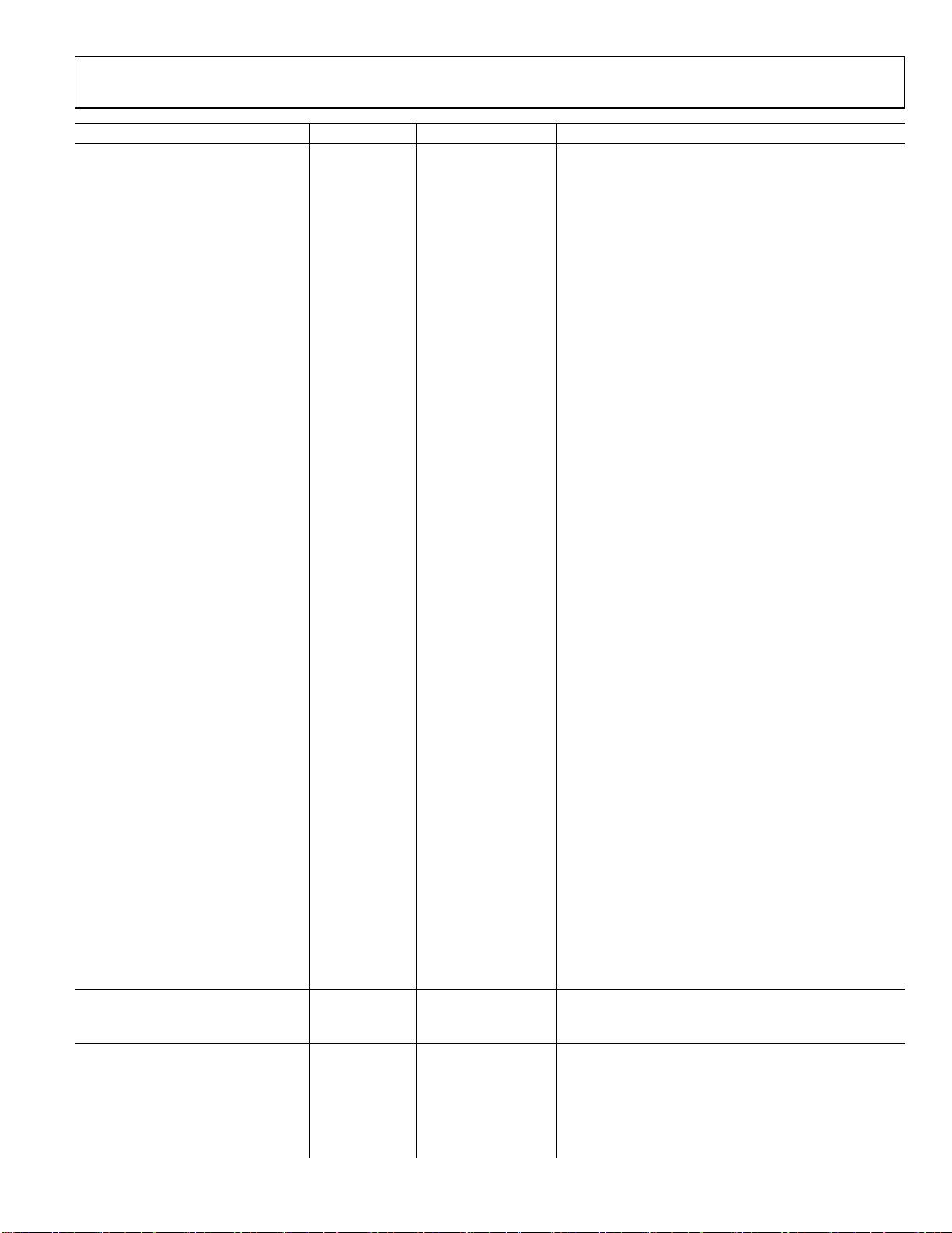
Preliminary Technical Data AD5751
Parameter Value1 Unit Test Conditions/Comments
4 to 20 mA
ACCURACY
Total Unadjusted Error (TUE) ±0.1 % FSR max With External Precision Resistor
TUE TC ±5 ppm max
Unipolar Output
Relative Accuracy (INL) ±0.02 % FSR max
Offset Error 0.01 % FSR max Error at analog input = 100mv (?)
Zero Scale Error 0.01 % FSR max Error at analog input = 0.0v
Zero Scale TC TBD ppm % FSR max
Gain Error 0.15 % FSR max (Ideal Span – Measured Span)/Ideal Span
Gain Error TC TBD ppm % FSR max
Full Scale Error 0.01 % FSR max Error at analog input = 4.096v (FS)
Full Scale Error TC TBD ppm % FSR max
Total Unadjusted Error (TUE) ±0.3 % FSR max With Internal Resistor
TUE TC ±20
±50
Unipolar Output
Relative Accuracy (INL) ±0.02 % FSR max
Offset Error 0.01 % FSR max Error at analog input = 100mv (?)
Zero Scale Error 0.01 % FSR max Error at analog input = 0.0v
Zero Scale TC TBD ppm % FSR max
Gain Error 0.15 % FSR max (Ideal Span – Measured Span)/Ideal Span
Gain Error TC TBD ppm % FSR max
Full Scale Error 0.01 % FSR max Error at analog input = 4.096v (FS)
Full Scale Error TC TBD ppm % FSR max
Output Current Ranges
(over range)
0.1 to 20.4 mA
3.9 to 20.4 mA
Relative Accuracy (INL) ±0.02 % FSR max
OUTPUT CHARACTERISTICS
Current Loop Compliance Voltage AVDD – 2.5 V max
Resistive Load See Comment kΩ max Chosen such that compliance is not exceeded.
Inductive Load 0.1 H max
0.1% Settling Time
DC PSRR 1 μA/V max
Output Impedance 25 MΩ typ
REFERENCE INPUT
Reference Input
Reference Input Voltage 4.096 V nom ±1% for specified performance
Input Leakage Current 1 uA max
DIGITAL INPUTS
VIH, Input High Voltage 2 V min
0.1 to 24.5 mA Nominal Over-ranges. See Text Page..
10 us
DVCC = 2.7 V to 5.5 V, JEDEC compliant
ppm typ
ppm max
Rev. PrA | Page 5 of 22
With External Precision Resistor
With Internal Resistor
Page 6
AD5751 Preliminary Technical Data
Parameter Value1 Unit Test Conditions/Comments
VIL, Input Low Voltage 0.8 V max
Input Current ±1 μA max Per pin
Pin Capacitance 10 pF typ Per pin
DIGITAL OUTPUTS
FAULT, IFAULT, TEMP, VFAULT
VOL, Output Low Voltage 0.4 V max
VOL, Output Low Voltage 0.6 V typ @ 2.5 mA
VOH, Output High Voltage 3.6 V min
SDO
VOL, Output Low Voltage 0.5 V max Sinking 200ua
VOH, Output High Voltage DVCC-0.5 V min Sourcing 200ua
High Impedance Leakage
current
High Impedance Output
Capacitance
POWER REQUIREMENTS
AVDD 12 to 24 V min to V max +/-10%
DVCC
Input Voltage 2.7 to 5.5 V min to V max Internal supply disabled
AVDD TBD mA Output unloaded
DICC TBD mA max VIH = DVCC, VIL = GND, TBD mA typ
Power Dissipation TBD mW typ
1
Temperature range: -40°C to +105°C; typical at +25°C.
10kΩ pull-up resistor to DV
10kΩ pull-up resistor to DV
±TBD ua max
20 pF max
CC
CC
TIMING CHARACTERISTICS
AVDD=12V (+/-10%) to +60V (MAX) , DVCC =2.7 V to 5.5 V, GND = 0 V. RL = 2 kΩ, CL = 200 pF, IOUT : RL = 300Ω, HL =
50mH All specifications T
Table 3.
Parameter
1, 2
Limit at T
t1 33 ns min SCLK cycle time
t2 13 ns min SCLK high time
t3 13 ns min SCLK low time
t4 13 ns min
t5 13 ns min
t6 100 ns min
t7 5 ns min Data setup time
MIN
to T
, unless otherwise noted.
MAX
, T
MIN
Unit Description
MAX
falling edge to SCLK falling edge setup time
SYNC
th
SCLK falling edge to SYNC rising edge
16
Minimum SYNC
Rev. PrA | Page 6 of 22
high time (WRITE MODE)
Page 7
Preliminary Technical Data AD5751
V
T
t8 0 ns min Data hold time
t10 , t9 1 μs max CLEAR pulse high/low activation time
t11 200 ns min
t
25 ns max SCLK rising edge to SDO valid (SDO CL=20pf)
12
t
1 us max CLEAR pulse low activation time
13
1 Guaranteed by characterization. Not production tested.
2 All input signals are specified with t
= tF = 5 ns (10% to 90% of DVCC) and timed from a voltage level of 1.2 V.
R
Minimum SYNC
high time (READ MODE)
O OUTPUT
PIN
C
15pF
200µA I
L
200µA I
SDO Load Timing.
OL
OH(min)-VOL(max)
2
OH
Rev. PrA | Page 7 of 22
Page 8

AD5751 Preliminary Technical Data
SCLK
SCLK
SYNC
SDIN
CLEAR
V
OUT
t
1
12 16
t
6
t
4
t
7
DB15
t
3
t
8
t
10
t
2
Figure 2. Write Mode Timing Diagram
21
DB0
t
5
t
9
16
SYNC
SDIN
SDO
t
11
A2
t
X
R=1 0
12
X
X
X
X
R3
A0
A1
XX
X
R2 R1
X
X
CLRSEL
R0
X
OUTEN
X
OVER
PEC
RSEL
Error
TEMP
X
XXX
VOUT
IOUT
Fault
Fault
Figure 3. Readback Mode Timing Diagram
Rev. PrA | Page 8 of 22
Page 9

Preliminary Technical Data AD5751
ABSOLUTE MAXIMUM RATINGS
TA = 25°C unless otherwise noted.
Transient currents of up to 100 mA do not cause SCR latch-up.
Table 4.
Parameter Rating
AVDD to GND −0.3V to 60v
DVCC to GND −0.3 V to +7 V
Digital Inputs to GND
−0.3 V to DV
+ 0.3 V or 7 V
CC
(whichever is less)
Digital Outputs to GND
−0.3 V to DV
+ 0.3 V or 7V
CC
(whichever is less)
REFIN/REFOUT to GND −0.3 V to +5 V
+V
to GND to AVDD
SENSE
VIN to GND −0.3 V to +5 V
V
to GND to AVDD
OUT
I
to GND −0.3V to AV
OUT
DD.
Operating Temperature Range
Industrial −40°C to +105°C
Storage Temperature Range −65°C to +150°C
Junction Temperature (TJ max) 125°C
32-Lead LFCSP Package
θJA Thermal Impedance 28°C/W
Lead Temperature JEDEC Industry Standard
Soldering J-STD-020
Stresses above those listed under Absolute Maximum Ratings
may cause permanent damage to the device. This is a stress
rating only; functional operation of the device at these or any
other conditions above those indicated in the operational
section of this specification is not implied. Exposure to absolute
maximum rating conditions for extended periods may affect
device reliability.
ESD CAUTION
Rev. PrA | Page 9 of 22
Page 10

Preliminary Technical Data AD5751
P
PIN CONFIGURATION AND FUNCTION DESCRIPTIONS
SELECT
C
N
NC
NC
NC
HW
RESET
NC/IFAULT
FAULT/TEM
29
28
27
26
31
30
32
25
SDO/VFAULT
SYNC/RSEL
SCLK/OUTEN
NC = NO CONN E CT
CLRSEL
CLEAR
DVCC
GND
SDIN/R0
1
PIN 1
2
INDICATOR
3
4
5
TOP VIEW
6
7
8
9
11
12
10
13
/R1
D0/R3
D2
D1/R2
REXT1
REXT2
24
SENSE+
V
VOUT
23
GND
22
21
GND
COMP1
20
COMP2
19
IOUT
18
17
AVDD
14
15
16
VIN
GND
VREF
00000-000
Figure 4. LFCSP Pin Configuration
Table 5. Pin Function Descriptions
LFCSP Pin No. Mnemonic Description
1 SDO/VFAULT
In Software Mode, Serial Data Output. Used to clock data from the serial register in
readback mode. Data is clocked out on the rising edge of SCLK and is valid on the
falling edge of SCLK. Open Drain Output, must be connected to a pull up resistor.
In Hardware mode, acts as a SHORT circuit Fault alert pin. This pin is asserted low when
an SHORT circuit. Error is detected. Open drain output, must be connected to a pull-up
resistor.
2 CLRSEL
In Hardware or software mode, selects the clear value, either zero-scale or mid-scale
code. In Software mode, this pin is implemented as a logic OR with the internal CLRSEL
bit.
3 CLEAR
Active High Input. Asserting this pin sets the Output Current/Voltage to zero-scale code
or mid-scale code of range selected (user-selectable). CLEAR is a LOGIC OR with the
internal CLEAR bit.
4 DVCC Digital Power Supply
5 GND Ground Connection.
6 SYNC/RSEL
In Software Mode, Positive edge sensitive latch, a rising edge will parallel load the input
shift register data into the INPUT register, also updating the output.
In Hardware mode, this pin chooses whether internal/external current sense resistor is
used
7 SCLK/OUTEN
In Software Mode, Serial Clock Input. Data is clocked into the shift register on the falling
edge of SCLK. This operates at clock speeds up to 30 MHz.
In Hardware mode, this pin acts as an output enable pin.
8 SDIN/RO In Software Mode, Serial Data Input. Data must be valid on the falling edge of SCLK.
In Hardware Mode, R0 is Range Decode Bit. This pin, in conjunction with R2, R3, R1
choose the output current/voltage range setting on the part.
9 AD2/R1
In Software Mode, AD2 is Device Addressing bit. This pin, in conjunction with AD1, AD0
allow up to 8 devices to be addressed on one bus.
In Hardware Mode, R1 is Range Decode Bit. This pin, in conjunction with R2, R3, R0
choose the output current/voltage range setting on the part.
10 AD1/R2
In Software Mode, AD1 is Device Addressing bit. This pin, in conjunction with AD2, AD0
allow up to 8 devices to be addressed on one bus.
Rev. PrA | Page 10 of 22
Page 11

Preliminary Technical Data AD5751
LFCSP Pin No. Mnemonic Description
In Hardware Mode, R2 is Range Decode Bit. This pin, in conjunction with R3, R1, R0
choose the output current/voltage range setting on the part.
11 AD0/R3
12
13
REXT1
REXT 2
14 VREF Reference Input
15 VIN Analog Input (0-4.096v)
16 GND Ground Connection.
17 AVDD Positive Analog Supply Pin.
18 IOUT Current Output Pin
19 COMP1 Optional compensation capacitor connection for the voltage output buffer
20 COMP2 Optional compensation capacitor connection for the voltage output buffer
21 GND Ground Connection.
22 GND Ground Connection.
23 V
24 +V
Buffered Analog Output Voltage.
OUT
Sense connection for the positive voltage output load connection.
SENSE
25,26,27,28 NC No Connect Pin. Can be tied to GND.
29 HW SELECT This part is used to configure the part to hardware/software mode.
30 RESET
31 FAULT/TEMP
32 NC/IFAULT
In Software Mode, AD0 is Device Addressing bit. This pin, in conjunction with AD1, AD2
allow up to 8 devices to be addressed on one bus.
In Hardware Mode, R3 is Range Decode Bit. This pin, in conjunction with R2, R1, R0
choose the output current/voltage range setting on the part.
An external current setting resistor can be connected to this pin to improve the I
OUT
temperature drift performance.
When using the Internal RSET resistor these pins must be left floating.
HW SELECT = 0 selects Software Control.
HW SELECT = 1 selects Hardware Control.
In software mode, resets the part to its power on state. Active low.
In hardware mode, there is no RESET. If using the part in hardware mode the RESET
pin should be tied high.
In Software mode, acts as a general Fault alert pin. This pin is asserted low when an
open circuit, short circuit, over temperature or PEC Interface Error is detected. Open
drain output, must be connected to a pull-up resistor.
In Hardware mode, acts as an over temp FAULT pin. This pin is asserted low when an
over temperature Error is detected. Open drain output, must be connected to a pull-up
resistor.
In Hardware mode, acts as a OPEN circuit Fault alert pin. This pin is asserted low when
an OPEN circuit. Error is detected. Open drain output, must be connected to a pull-up
resistor.
In Software mode, is a NC. Tie to GND.
Rev. PrA | Page 11 of 22
Page 12

AD5751 Preliminary Technical Data
TYPICAL PERFORMANCE CHARACTERISTICS
Figure 5.
Figure 6.
Figure 8.
Figure 9.
Figure 7.
Rev. PrA | Page 12 of 22
Figure 10
Page 13

AD5751 Preliminary Technical Data
MCU
SCLK
SDI
SDO
SYNC1
LDO
VDD
AD566X
ADR392
REFIN
DVCC
REFIN
VIN
HW SELECT
OUTEN
TEMP
VDD AGND
AD5751
VFAULT*
IFAULT*
VOUT
RANGE
SCALE
IOUT
RANGE
SCALE
VSENSE+
VSENSE-
R3
R2
R1
R0
VOUT
0-5V, 0-10V ,
IOUT
0-20ma, 0-24m a,
4-20ma.
OUTPUT
RANGE
SELECT
PINS
Figure 12. Typical System Configuration in Hardware Mode. Pull up resistors not shown for open drain outputs.
Rev. PrA | Page 13 of 22
Page 14

AD5751 Preliminary Technical Data
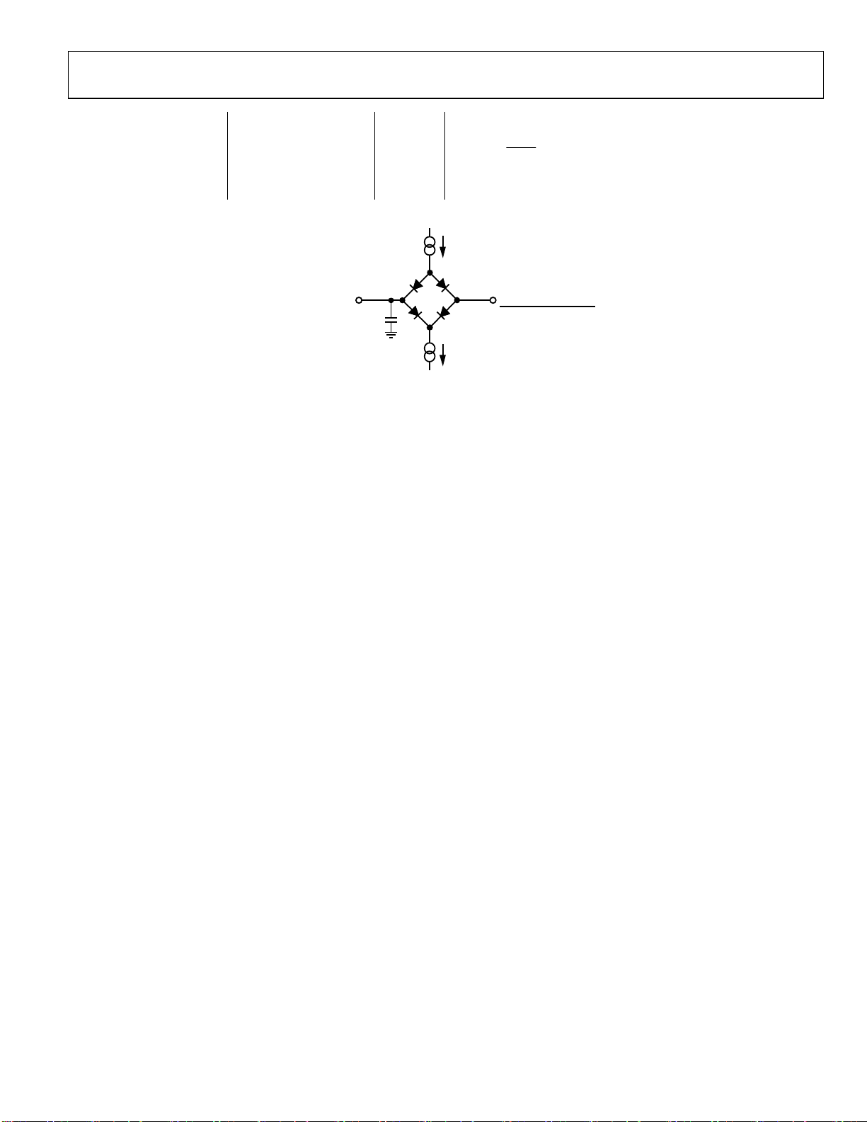
CURRENT OUTPUT ARCHITECTURE
The voltage input from the analog input VIN core (0-4.096v) is
either converted to a current (see Figure 11) which is then
mirrored to the supply rail so that the application simply sees a
current source output with respect to an internal reference
voltage or it is buffered and scaled to output a software
selectable unipolar voltage range (See Figure 12). The
Reference is used to provide internal offsets for range and gain
scaling. The selectable output range is programmable through
the digital interface.
VIN
VREF
VIN
(0-4.096V)
VREF
Voltage Output Amplifier
The voltage output amplifier is capable of generating both
unipolar and bipolar output voltages. It is capable of driving a
load of 1 kΩ in parallel with 1.2 uF. The source and sink
capabilities of the output amplifier can be seen in Figure TBD.
The slew rate is 1 V/μs with a full-scale settling time of 10
μs.(10V step).
The current and voltage are output on separate pins and cannot
be output simultaneously. This allows the user to tie both the
current and voltage output pins together and configuring the
end system as “one channel” output.
Driving Large Capacitive Loads
The voltage output amplifier is capable of driving capacative
loads of up to 1uF with the addition of a non-polarised 4nF
compensation capacitor between the C
Without the compensation capacitor, up to 20nF capacitive
loads can be driven.
RANGE DECODE
FROM INTERFACE
IOUT
RANGE
SCALING
Figure 11. Current Output Configuration
RANGE DECODE
FROM INTERFACE
VOUT RANGE
SCALING
Figure 12. Voltage Output
T1
A1
VOUT SHORT FAULT
and C
COMP1
AVDD
R2
R1
A2
COMP2
R3
T2
I
+VSENSE
VOUT
-VSENSE
pins.
OUT
POWER ON STATE OF AD5751
On Power-up, the AD5751 will sense whether hardware or
software mode is loaded and set the power up conditions
accordingly.
In software SPI mode, the part will power up with all outputs
disabled (OUTEN bit=0). In disabled mode, both the current
and voltage outputs are put into tri-state mode. The user will
have to set the OUTEN bit in the control register to enable the
output and in the same write the user will also set the output
range configuration using the range bits.
If hardware mode is selected, the part will power up to the
conditions defined by the range bits and the status of the
OUTEN pin. It is recommended to keep the output disabled
when powering up the part in hardware mode.
RESET:
The AD5750 contains a reset function.
In Software mode, the part can be reset using the RESET pin
(active low) or the RESET bit (RESET=1). A reset will disable
both the current and voltage outputs. The user will have to
write to the OUTEN bit to enable the output and in the same
write the user will also set the output range configuration. The
RESET pin is a level sensitive input - the part will stay in
RESET mode as long as RESET pin is low. The RESET bit
will clear to zero following a RESET command to the control
register.
In hardware mode, there is no RESET. If using the part in
hardware mode the RESET pin should be tied high.
OUTEN
In Software mode, the output can be enabled/disabled using the
OUTEN bit in the control register. When the output is disabled,
both the current and voltage channels both go into tri-state. The
user will have to set the OUTEN bit to enable the output and at
this time the user will also set the output range configuration.
In Hardware mode, the output can be enabled/disabled using
the OUTEN pin. When the output is disabled, both the current
and voltage channels both go into tri-state. The user will have
to write to the OUTEN pin to enable the output. It is
recommended that the output be disabled when changing the
ranges.
Rev. PrA | Page 14 of 22
Page 15

Preliminary Technical Data AD5751
SOFTWARE CONTROL:
Software control is enabled by connecting the HW SELECT pin to ground. In software mode, the AD5751 is controlled over a versatile 3wire serial interface that operates at clock rates up to 30 MHz. It is compatible with SPI®, QSPI™, MICROWIRE™, and DSP standards The
input shift register is 16 bits wide. Data is loaded into the device MSB first as a 16-bit word under the control of a serial clock input,
SCLK. Data is clocked in on the falling edge of SCLK. The input register consists of 16 control bits as shown in Table 5. The timing
diagram for this operation is shown in Figure 2. The first 3 bits of the Input Register are used to set the hardware address of the AD5751
device on the PCB board. Up to 8 devices can be addressed per board.
Bits D11, D1, D0 must always be set to 0 during any write or read sequence.
Table 3. Input Shift Register Format
MSB LSB
D15 D14 D13 D12 D11 D10 D9 D8 D7 D6 D5 D4 D3 D2 D1 D0
A2 A1 A0
Table 6. Input Shift Register Decoded
Register
A2, A1, A0
A2
R/W
CLEAR
CLRSEL
OUTEN
RSEL
R3,R2,R1,R0
RSEL R3
Used in association with External Pins AD2, AD1, AD0 to determine which part is
being addressed by the system controller.
0
0
0
0
1
1
1
1
Indicates a read from or a write to the addressed register.
Software Clear Bit – Active High.
Sets Clear Mode to zero scale or midscale. See Text.
CLRSEL
0
1
Output Enable Bit. This bit must be set to 1 to enable the outputs.
Select Internal/External Current Sense Resistor.
RSEL
1
0
Selects output Configuration in conjunction with RSEL.
0 0
0 0
0 0
0 0
0 0
0 0
0 0
0 0
0 1
0 1
0 R3 R2 R1 R0 CLRSEL OUTEN CLEAR RSEL RESET 0 0
R/
W
A1 A0 Function
0 0 Addresses Part with pins AD2=0, AD1=0, AD0=0
0 1 Addresses Part with pins AD2=0, AD1=0, AD0=1
1 0 Addresses Part with pins AD2=0, AD1=1, AD0=0
1 1 Addresses Part with pins AD2=0, AD1=1, AD0=1
0 0 Addresses Part with pins AD2=1, AD1=0, AD0=0
0 1 Addresses Part with pins AD2=1, AD1=0, AD0=1
1 0 Addresses Part with pins AD2=1, AD1=1, AD0=0
1 1 Addresses Part with pins AD2=1, AD1=1, AD0=1
Clear to Zero Volts
Clear to Mid Scale in Unipolar Mode, Clear to Zero Scale in Bipolar Mode.
Select Internal Current Sense Resistor /*used with Range bits to select Range */
Select External Current Sense Resistor /*used with Range bits to select Range */
R2 R1 R0 Output Configuration
0 0 0 4-20MA External Current Sense Resistor 15k ohm.
0 0 1 0-20MA External Current Sense Resistor 15k ohm.
0 1 0 0-24MA External Current Sense Resistor 15k ohm.
0 1 1 N/A. If selected output will drive 0V.
1 0 0 N/A. If selected output will drive 0V.
1 0 1 0-5V
1 1 0 0-10V
1 1 1 N/A. If selected output will drive 0V.
0 0 0 N/A. If selected output will drive 0V.
0 0 1 0-6.0V (20% over range)
Rev. PrA | Page 15 of 22
Page 16

AD5751 Preliminary Technical Data
Reset
Readback Operation
Readback mode is invoked by selecting the correct device address (A2,A1,A0) and then setting the R/W bit to 1. By default the SDO pin is
disabled, after having addressed the AD5751 for a read operation, setting R/W to 1 will enable the SDO pin and SDO data will be clocked
out on the 5
pin once again. STATUS and CONTROL register data will be both available during the same read cycle. See Table 7 below.
0 1
0 1
0 1
0 1
0 1
0 1
1 0
1 0
1 0
1 0
1 0
1 0
1 0
1 0
1 1
1 1
1 1
1 1
1 1
1 1
1 1
1 1
Resets the part to its Power on State
th
rising edge of SCLK. After the data has been clocked out on SDO, a rising edge on SYNC will disable (tri- state) the SDO
0 1 0 0-12.0V (20% over range)
0 1 1 N/A. If selected output will drive 0V.
1 0 0 N/A. If selected output will drive 0V.
1 0 1 N/A. If selected output will drive 0V.
1 1 0 0-40V
1 1 1 0-48V
0 0 0 4-20MA Internal Current Sense Resistor.
0 0 1 0-20MA Internal Current Sense Resistor.
0 1 0 0-24MA Internal Current Sense Resistor.
0 1 1 N/A. Output will revert to CLEAR condition.
1 0 0 N/A. Output will revert to CLEAR condition.
1 0 1 0-5V
1 1 0 0-10V
1 1 1 N/A. If selected output will drive 0V.
0 0 0 N/A. If selected output will drive 0V.
0 0 1 0-6.0V (20% over range)
0 1 0 0-12.0V (20% over range)
0 1 1 N/A. If selected output will drive 0V.
1 0 0 N/A. If selected output will drive 0V.
1 0 1 3.92ma – 20.4ma Internal Current Sense Resistor.
1 1 0 0ma – 20.4ma Internal Current Sense Resistor.
1 1 1 0ma – 24.5ma Internal Current Sense Resistor.
Table 7. Input Shift Register Contents for a read operation
MSB LSB
D15 D14 D13 D12 D11 D10 D9 D8 D7 D6 D5 D4 D3 D2 D1 D0
A2 A1 A0
0 R3 R2 R1 R0 CLRSEL OUTEN RSEL
1
PEC Error Bit
OVER TEMP IOUT Fault Vout Fault
The STATUS bits are 5 read only bits. They are used to notify the user of specific fault conditions that have arisen, such as open or short
circuit on the output, over temperature, interface error or a range error. If any one of these fault conditions are set then a general fault
error bit is set (bit D5). This bit also sets a FAULT pin which can be used as a hardware interrupt to the controller.
Full explanation of fault conditions are given in the Features sections.
Table 9. STATUS Bits Options
Option Description
PEC ERROR Bit Set if there is an Interface Error detected by CRC-8 Error Checking. See features section.
VOUT FAULT Bit set if there is a short Circuit on VOUT pin.
IOUT FAULT Bit set is there is an open circuit on IOUT pin.
OVER TEMP This bit will be set if the AD5750 core temperature exceeds approx. 150°C.
Rev. PrA | Page 16 of 22
Page 17
Preliminary Technical Data AD5751
HARDWARE CONTROL:
Hardware control is enabled by connecting the HW SELECT pin to DVCC. In this mode, pins R3,R2,R1,R0 along with RSEL pin are used
to configure the output range as per Table.
RSEL R3
0 0
0 0
0 0
0 0
0 0
0 0
0 0
0 0
0 1
0 1
0 1
0 1
0 1
0 1
0 1
0 1
1 0
1 0
1 0
1 0
1 0
1 0
1 0
1 0
1 1
1 1
1 1
1 1
1 1
1 1
1 1
1 1
In hardware mode there is no status register. The fault conditions; open circuit, short circuit and over temperature are available on pins
IFAULT, VFAULT and TEMP. If any one of these fault conditions are set then a low is asserted on the specific fault pin. IFAULT, VFAULT
and TEMP are open drain outputs and therefore can be connected together to allow the user generate one interrupt to the system
controller to communicate a fault. If hardwired in this way, it will not be possible to isolate which fault occurred in the system.
R2 R1 R0 Output Configuration
0 0 0 4-20MA External Current Sense Resistor 15k ohm.
0 0 1 0-20MA External Current Sense Resistor 15k ohm.
0 1 0 0-24MA External Current Sense Resistor 15k ohm.
0 1 1 N/A. If selected output will drive 0V.
1 0 0 N/A. If selected output will drive 0V.
1 0 1 0-5V
1 1 0 0-10V
1 1 1 N/A. If selected output will drive 0V.
0 0 0 N/A. If selected output will drive 0V.
0 0 1 0-6.0V (20% over range)
0 1 0 0-12.0V (20% over range)
0 1 1 N/A. If selected output will drive 0V.
1 0 0 N/A. If selected output will drive 0V.
1 0 1 N/A. If selected output will drive 0V.
1 1 0 0-40V
1 1 1 0-44V
0 0 0 4-20MA Internal Current Sense Resistor.
0 0 1 0-20MA Internal Current Sense Resistor.
0 1 0 0-24MA Internal Current Sense Resistor.
0 1 1 N/A. If selected output will drive 0V.
1 0 0 N/A. If selected output will drive 0V.
1 0 1 0-5V
1 1 0 0-10V
1 1 1 N/A. If selected output will drive 0V.
0 0 0 N/A. If selected output will drive 0V.
0 0 1 0-6.0V (20% over range)
0 1 0 0-12.0V (20% over range)
0 1 1 N/A. If selected output will drive 0V.
1 0 0 N/A. If selected output will drive 0V.
1 0 1 3.92ma – 20.4ma Internal Current Sense Resistor.
1 1 0 0ma – 20.4ma Internal Current Sense Resistor.
1 1 1 0ma – 24.5ma Internal Current Sense Resistor.
Rev. PrA | Page 17 of 22
Page 18

AD5751 Preliminary Technical Data
DEFAULT CONFIGURATION:
On initial power-up of the AD5751 the power-on-reset circuit ensures that all registers are loaded with zero-code, as such the default
output is the current output with the 4mA to 20mA range selected, the current output until a value is programmed is 0mA. The voltage
output pin will be in three-state. An alternative current range or a voltage output range may be selected via the CONTROL register.
Rev. PrA | Page 18 of 22
Page 19

Preliminary Technical Data AD5751
FEATURES
OUTPUT FAULT ALERT – SOFTWARE MODE
In Software mode, the AD5751 is equipped with one FAULT
pin, this is an open-drain output allowing several AD5751
devices to be connected together to one pull-up resistor for
global fault detection. In software control mode, the FAULT pin
is forced active high by any one of the following fault scenarios;
1) The Voltage at I
compliance range, due to an open-loop circuit or
insufficient power supply voltage. The internal
circuitry that develops the fault output avoids using a
comparator with “window limits” since this would
require an actual output error before the FAULT
output becomes active. Instead, the signal is generated
when the internal amplifier in the output stage has less
than approximately one volt of remaining drive
capability. Thus the FAULT output activates slightly
before the compliance limit is reached. Since the
comparison is made within the feedback loop of the
output amplifier, the output accuracy is maintained by
its open-loop gain and an output error does not occur
before the FAULT output becomes active.
2) A short is detected on the voltage output pin. Short
circuit current limited to 25ma.
3) An interface error is detected due to the PEC error
checking failure. See PEC error checking section.
4) A range change is detected without the user writing to
the Interface.
5) If the core temperature of the AD5751 exceeds approx.
150°C.
attempts to rise above the
OUT
OUTPUT FAULT ALERT – HARDWARE MODE
In Hardware mode, the AD5751 is equipped with 3 FAULT
pins, VFAULT, IFAULT, TEMP. These are an open-drain
outputs allowing several AD5751 devices to be connected
together to one pull-up resistor for global fault detection. In
hardware control mode, these fault pins are forced active by any
one of the following fault scenarios;
1) Open Circuit Detect. The Voltage at I
rise above the compliance range, due to an open-loop
circuit or insufficient power supply voltage. The
internal circuitry that develops the fault output avoids
using a comparator with “window limits” since this
would require an actual output error before the
FAULT output becomes active. Instead, the signal is
generated when the internal amplifier in the output
stage has less than approximately one volt of
remaining drive capability. Thus the FAULT output
activates slightly before the compliance limit is
reached. Since the comparison is made within the
attempts to
OUT
Rev. PrA | Page 19 of 22
VOLTAGE OUTPUT SHORT CIRCUIT PROTECTION
Under normal operation the voltage output will sink/source
5mA and maintain specified operation. The maximum current
that the voltage output will deliver is 25mA, this is the short
circuit current.
ASYNCHRONOUS CLEAR (CLEAR)
CLEAR is an active high clear that allows the voltage output to
be cleared to either zero-scale code or mid-scale code, userselectable via the CLRSEL pin or the CLRSEL bit of the INPUT
register as described in Table 6. (The Clear select feature is a
logical OR function of the CLR SELECT pin and the CLRSEL
bit). The Current loop output will clear to the bottom of its
programmed range. It is necessary to maintain CLEAR high for a
minimum amount of time (see Figure 2) to complete the
operation. When the CLEAR signal is returned low, the output
returns to its programmed value or a new value if programmed.
A clear operation can also be performed via the CLEAR
command in the control register.
Table 11. CLEAR SELECT Options
CLR
SELECT
Unipolar Output Voltage
0 0 V
1 Mid-Scale
Unipolar Current Output
0 Zero-Scale e.g.
1 Mid-Scale e.g.
feedback loop of the output amplifier, the output
accuracy is maintained by its open-loop gain and an
output error does not occur before the FAULT output
becomes active.
If this fault is detected the IFAULT pin is forced low.
2) A short is detected on the voltage output pin. Short
circuit current limited to 25ma. If this fault is detected
the VFAULT pin is forced low.
3) If the core temperature of the AD5751 exceeds approx.
150°C. If this fault is detected the TEMP pin is forced
low.
Output CLR Value
Range
Range
4ma on 4-20ma
0ma on 0-20ma etc...
12ma on 4-20ma
10ma on 0-20ma
Page 20

AD5751 Preliminary Technical Data
EXTERNAL CURRENT SETTING RESISTOR
Referring to Figure 1, RSET is an internal sense resistor as part
of the voltage to current conversion circuitry. The stability of
the output current value over temperature is dependent on the
stability of the value of RSET. As a method of improving the
stability of the output current over temperature an external low
drift resistor can be connected to the RSET pin of the AD5751
to be used instead of the internal resistor RSET. The external
resistor is selected via the input register in software mode or by
setting the RSEL bit in hardware mode. If the external resistor
option is not used the RSET pin should be left floating.
OVER-RANGE MODES
The AD5751 contains an over range mode for most of the
available ranges. In voltage mode the over-range is typically
20% (10% for 0-40v range) and in current mode the over-range
is typically 2%. The overranges are selected by configuring R3,
R1, R1, R0 bits/pins accordingly.
In voltage mode the overranges are typically 20% providing
programmable output ranges of 0-6v, 0-12v, 0-44v The 0-4.096v
analog input remains the same.
In current mode the overranges are typically 2%. In current
mode the overrange capability is only available on 3 ranges, 020ma, 0-24ma, 4-20ma. For these ranges the analog input will
also vary, according to the table below.
Over Range Analog Input
0-20.4ma 0.075v – 4.096v
3.92-20.4ma 0.06v-4.096v
0-24.5ma 0.065-4.096v
PACKET ERROR CHECKING
To verify that data has been received correctly in noisy
environments, the AD5751 offers the option of error
checking based on an 8-bit (CRC-8) cyclic redundancy check.
The device controlling the AD5751 should generate an 8-bit
frame check sequence using the polynomial
C(x) = x
This is added to the end of the data word, and 24 data
8 + x2 + x1 +1.
bits are sent to the AD5751 before taking SYNC high.
If the AD5751 sees a 24-bit data frame, it will perform
the error check when SYNC goes high. If the check is valid,
then the data will be written to the selected register. If the error
check fails, the FAULT will go high and bit D4 of the Status
Register is set. After reading this register, this error flag is
cleared automatically and PEC goes high again.
SYNC
SCLK
DIN
SYNC
SCLK
DIN
PEC
UPDATE ON SYNC HIGH
MSB
D15
MSB
D23
Figure 13. PEC Error Checking Timing
16-BIT DATA
16-BIT DATATRANSFER - NO ERROR CHECKING
16 BIT DATA
16-BIT DATA TRANSFER WITH ERROR CHECKING
LSB
D0
UPDATE AFTER SYNC HIGH
ONLY IF ERROR CHECK PASSED
LSB
D7
D8
PEC GOES LOWIF
ERROR CHECK FAILS
D0
8-BIT FCS
Rev. PrA | Page 20 of 22
Page 21

Preliminary Technical Data AD5751
APPLICATIONS INFORMATION
TRANSIENT VOLTAGE PROTECTION
The AD5751 contains ESD protection diodes which prevent
damage from normal handling. The industrial control
environment can, however, subject I/O circuits to much higher
transients. In order to protect the AD5751 from excessively high
voltage transients , external power diodes and a surge current
limiting resistor may be required, as shown in Figure 15. The
constraint on the resistor value is that during normal operation
the output level at IOUT must remain within its voltage
compliance limit of AV
– 2.0V and the two protection diodes
DD
and resistor must have appropriate power ratings.
AV
DD
AV
DD
AD5751
I
OUT
Figure 15. Output Transient Voltage Protection
R
P
R
LOAD
LAYOUT GUIDELINES
In any circuit where accuracy is important, careful consideration
of the power supply and ground return layout helps to ensure
the rated performance. The printed circuit board on which the
AD5751 is mounted should be designed so that the AD5751 lies
on the analog plane.
The AD5751 should have ample supply bypassing of 10 μF in
parallel with 0.1 μF on each supply located as close to the
package as possible, ideally right up against the device. The 10
μF capacitors are the tantalum bead type. The 0.1 μF capacitor
should have low effective series resistance (ESR) and low
effective series inductance (ESI) such as the common ceramic
types, which provide a low impedance path to ground at high
frequencies to handle transient currents due to internal logic
switching.
The power supply lines of the AD5751 should use as large a
trace as possible to provide low impedance paths and reduce the
effects of glitches on the power supply line. Fast switching
signals such as clocks should be shielded with digital ground to
avoid radiating noise to other parts of the board and should
never be run near the reference inputs. A ground line routed
between the SDIN and SCLK lines helps reduce crosstalk
between them (not required on a multilayer board that has a
separate ground plane, but separating the lines helps). It is
essential to minimize noise on the REFIN line.
Avoid crossover of digital and analog signals. Traces on
opposite sides of the board should run at right angles to each
other. This reduces the effects of feed through the board. A
microstrip technique is by far the best, but not always possible
with a double-sided board. In this technique, the component
side of the board is dedicated to ground plane, while signal
traces are placed on the solder side.
GALVANICALLY ISOLATED INTERFACE
In many process control applications, it is necessary to provide
an isolation barrier between the controller and the unit being
controlled to protect and isolate the controlling circuitry from
any hazardous common-mode voltages that might occur. The
iCoupler® family of products from Analog Devices provides
voltage isolation in excess of 2.5 kV. The serial loading structure
of the AD5751 make it ideal for isolated interfaces because the
number of interface lines is kept to a minimum. Figure 16 shows
a 4-channel isolated interface to the AD5751 using an
ADuM1400. For further information, visit
http://www.analog.com/icouplers.
Controller
Serial Clock Out
Serial Data Out
SYNC Out
Control out
*ADDITIONAL PINS OM I T T ED FOR CLARIT Y
ADuM1400 *
V
IA
ENCODE DECODE
V
IB
ENCODE DECODE
V
IC
ENCODE DECODE
V
ID
ENCODE DECODE
Figure16. Isolated Interface
V
OA
V
OB
V
OC
V
OD
To SCLK
To SDIN
To SYNC
To CLEA R
MICROPROCESSOR INTERFACING
Microprocessor interfacing to the AD5751 is via a serial bus that
uses protocol compatible with microcontrollers and DSP
processors. The communications channel is a 3-wire
(minimum) interface consisting of a clock signal, a data signal,
and a sync signal. The AD5751 require a 16-bit data-word with
data valid on the falling edge of SCLK.
Rev. PrA | Page 21 of 22
Page 22

AD5751 Preliminary Technical Data
OUTLINE DIMENSIONS
0.08
0.60 MAX
25
24
EXPOSED
PAD
(BOTTOM VIEW)
17
16
32
1
8
9
3.50 REF
PIN 1
INDICATOR
3.25
3.10 SQ
2.95
0.25 MIN
5.00
INDICATOR
1.00
0.85
0.80
PIN 1
12° MAX
SEATING
PLANE
BSC SQ
TOP
VIEW
0.80 MAX
0.65 TYP
0.30
0.23
0.18
COMPLIANT TO JEDEC STANDARDS MO-220-VHHD-2
4.75
BSC SQ
0.20 REF
0.05 MAX
0.02 NOM
0.60 MAX
0.50
BSC
0.50
0.40
0.30
COPLANARITY
Figure 17. 32-Lead Lead Frame Chip Scale Package
(CP-32-2)
Dimensions shown in millimeters
ORDERING GUIDE
Model Temperature Range Package Description Package Option
AD5751BCPZ -40°C to 105°C 32 Lead LFCSP CP-32-2
Rev. PrA | Page 22 of 22 PR07269-0-5/08(PrA)
 Loading...