

Page 1

Industrial Current/Voltage Output Driver
with Programmable Ranges
AD5750/AD5750-1/AD5750-2
Rev. E
Trademarks and registered trademarks are the property of their respective owners.
Fax: 781.461.3113 ©2009–2012 Analog Devices, Inc. All rights reserved.
maximum supply, programmable ranges
AD5420
Single channel, 16-bit, serial input, 4 mA to
Data Sheet
FEATURES
Current output ranges: 4 mA to 20 mA, 0 mA to 20 mA, 0 mA
to 24 mA, ±20 mA, and ±24 mA
±0.03% full-scale range (FSR) total unadjusted error (TUE)
±5 ppm/°C typical output drift
Voltage output ranges: 0 V to 5 V, 0 V to 10 V, ±5 V, and ±10 V
with 20% overrange
±0.02% FSR TUE
±3 ppm/°C typical output drift
Flexible serial digital interface
On-chip output fault detection
Packet error checking (PEC)
Asynchronous CLEAR function
Flexible power-up condition to 0 V or tristate
Power supply range
AV
: +12 V (± 10%) to +24 V (± 10%)
DD
AV
: −12 V (± 10%) to −24 V (± 10%)
SS
Output loop compliance to AV
Temperature range: −40°C to +105°C
32-lead, 5 mm × 5 mm LFCSP package
APPLICATIONS
Process controls
Actuator controls
PLCs
GENERAL DESCRIPTION
The AD5750/AD5750-1/AD5750-2 are single-channel, low cost,
precision voltage/current output drivers with hardware- or
software-programmable output ranges. The software ranges are
configured via an SPI-/MICROWIRE™-compatible serial interface.
The AD5750/AD5750-1/AD5750-2 target applications in PLC
and industrial process control. The analog input to the AD5750/
AD5750-1/AD5750-2 is provided from a low voltage, single-supply
digital-to-analog converter (DAC) and is internally conditioned
to provide the desired output current/voltage range. Analog input
ranges available are 0 V to 2.5 V (AD5750-1/AD5750-2) or 0 V
to 4.096 V (AD5750).
− 2.75 V
DD
The output current range is programmable across five current
ranges: 4 mA to 20 mA, 0 mA to 20 mA, 0 mA to 24 mA, ±20 mA,
and ±24 mA. An overrange of 2% is available on the unipolar
current ranges.
Voltage output is provided from a separate pin that can be
configured to provide 0 V to 5 V, 0 V to 10 V, ±5 V, or ±10 V
output ranges. An overrange of 20% is available on the voltage
ranges.
Analog outputs are short-circuit and open-circuit protected and
can drive capacitive loads of 1 µF and inductive loads of 0.1 H.
The devices are specified to operate with a power supply range
from ±12 V to ±24 V. Output loop compliance is 0 V to AV
DD
−
2.75 V.
The flexible serial interface is SPI and MICROWIRE compatible
and can operate in 3-wire mode to minimize the digital isolation
required in isolated applications. The interface also features an
optional PEC feature using CRC-8 error checking, useful in
industrial environments where data communication corruption
can occur.
The devices also include a power-on-reset function, ensuring that
the devices power up in a known state (0 V or tristate), and an
asynchronous CLEAR pin that sets the outputs to a zero scale/midscale voltage output or the low end of the selected current range.
The HW SELECT pin is used to configure the parts for hardware
or software mode on power-up.
Table 1. Related Devices
Part Number Description
AD5422 Single channel, 16-bit, serial input current
source and voltage output DAC
AD5751 Industrial I/V output driver, single supply, 55 V
20 mA current source DAC
Information furnished by Analog Devices is believed to be accurate and reliable. However, no
responsibility is assumed by Analog Devices for its use, nor for any infringements of patents or other
rights of third parties that may result from its use. Specifications subject to change without notice. No
license i s granted by implication or otherwise under any patent or patent rights of Analog Devices.
One Technology Way, P.O. Box 9106, Norwood, MA 02062-9106, U.S.A.
Tel: 781.329.4700
www.analog.com
Page 2

AD5750/AD5750-1/AD5750-2 Data Sheet
TABLE OF CONTENTS
Features .............................................................................................. 1
Applications ....................................................................................... 1
General Description ......................................................................... 1
Revision History ............................................................................... 2
Functional Block Diagram .............................................................. 3
Specifications ..................................................................................... 4
Timing Characteristics ................................................................ 8
Absolute Maximum Ratings .......................................................... 10
ESD Caution ................................................................................ 10
Pin Configuration and Function Descriptions ........................... 11
Typical Performance Characteristics ........................................... 13
Voltage Output ............................................................................ 13
Current Output ........................................................................... 17
Terminology .................................................................................... 22
Theory of Operation ...................................................................... 23
Software Mode ............................................................................ 23
Current Output Architecture .................................................... 25
Driving Inductive Loads ............................................................ 25
Power-On State of AD5750/AD5750-1/AD5750-2 ................... 25
Default Registers at Power-On ................................................. 26
Reset Function ............................................................................ 26
OUTEN ........................................................................................ 26
Software Control ........................................................................ 26
Hardware Control ...................................................................... 28
Transfer Function ....................................................................... 28
Detailed Description of Features .................................................. 29
Output Fault Alert—Software Mode ....................................... 29
Output Fault Alert—Hardware Mode ..................................... 29
Voltage Output Short-Circuit Protection ................................ 29
Asynchronous Clear (CLEAR) ................................................. 29
External Current Setting Resistor ............................................ 30
Programmable Overrange Modes ............................................ 30
Packet Error Checking ............................................................... 30
Applications Information .............................................................. 31
Transient Voltage Protection .................................................... 31
Thermal Considerations ............................................................ 31
Layout Guidelines....................................................................... 31
Galvanically Isolated Interface ................................................. 32
Microprocessor Interfacing ....................................................... 32
Outline Dimensions ....................................................................... 33
Ordering Guide .......................................................................... 33
REVISION HISTORY
6/12—Rev. D to Rev. E
Changes to Figure 3 .......................................................................... 9
Changes to Status Bit Read Operation Section ........................... 28
Updated Outline Dimensions ....................................................... 33
4/12—Rev. C to Rev. D
Added AD5750-2 ................................................................ Universal
Changes to Table 2 ............................................................................ 4
Updated Outline Dimensions ....................................................... 33
Changes to Ordering Guide .......................................................... 33
7/10—Rev. B to Rev. C
Added Leakage Current in Voltage Output Characteristics
Parameter (Table 2) .......................................................................... 5
Added Leakage Current in Current Output Characteristics
Parameter (Table 2) .......................................................................... 6
6/10—Rev. A to Rev. B
Changes to Table 1 ............................................................................ 1
Changes to Table 2, Power Requirements ..................................... 7
Rev. E | Page 2 of 36
8/09—Rev. 0 to Rev. A
Added AD5750-1................................................................ Universal
Changes to Features and General Description Sections .............. 1
Changes to Table 2 ............................................................................. 4
Changes to Theory of Operation Section and Figure 51 .......... 23
Change to Figure 52 and Table 6 Title ......................................... 24
Changes to Current Output Architecture Section and Power-On
State of AD5750/AD5750-1 .......................................................... 25
Changes to Transfer Function Section ........................................ 28
Changes to Programmable Overrange Modes Section ............. 30
Changes to Ordering Guide .......................................................... 33
7/09—Revision 0: Initial Version
Page 3
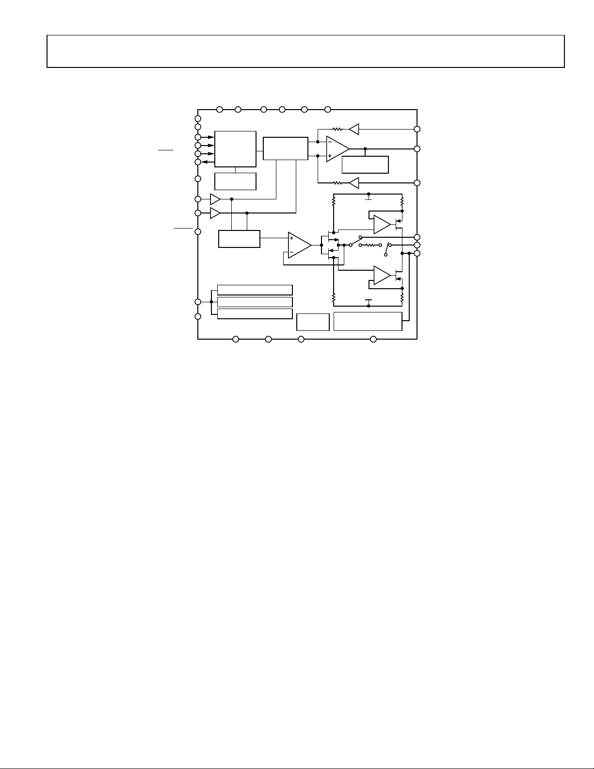
Data Sheet AD5750/AD5750-1/AD5750-2
CLEAR
VSENSE+
VOUT
VSENSE–
REXT1
IOUT
DV
CC
GND
AVDDGND
COMP1 COMP2
AD2/R1* AD1/R2*
AD0/R3* AV
SS
CLRSEL
HW SELECT
VIN
VREF
SCLK/OUTEN*
SDIN/R0*
SYNC/RSET*
SDO/VFAULT*
INPUT SHIFT
REGISTER
AND
CONTROL
LOGIC
STATUS
REGISTER
VOUT RANGE
SCALING
IOUT RANG E
SCALING
VOUT
SHORT FAULT
POWER-
ON RESET
FAULT/TEMP*
NC/IFAULT*
OVERTEMP
VOUT SHO RT FAULT
IOUT OPENFAULT
RESET
R
SET
Vx**
V
SS
V
DD
R2 R3
REXT2
IOUT
OPEN FAULT
AD5750/AD5750-1/AD5750-2
*DENOTES S HARE D P IN. SOF TWARE MODE DE NOTED BY REGUL AR TEXT, HARDWARE MODE
DENOTED BY ITALIC TEXT. FOR EXAMPLE, FOR FAULT/ TEMP PIN, IN SOFTWARE MODE, THIS
PIN TAKES ON FAULT FUNCTION. IN HARDWARE MODE, THIS PIN TAKES ON TEMP FUNCTION.
**Vx IS AN I NTERNAL BIAS V OLTAG E ( CAN BE GROUND OR OT HE R V O LTAGE) T HAT IS USED
TO GENERATE THE INTERNAL SENSE CURRENT S NE E DE D FOR THE CURRENT OUTPUTS.
07268-001
FUNCTIONAL BLOCK DIAGRAM
Figure 1.
Rev. E | Page 3 of 36
Page 4

AD5750/AD5750-1/AD5750-2 Data Sheet
INPUT VOLTAGE RANGE
Output unloaded
−5 +5 V
Bipolar Zero Error (Offset at Midscale)
−10 +10
mV
±10 V range
SPECIFICATIONS
AVDD/AVSS = ±12 V (± 10%) to ±24 V (± 10%), DVCC = 2.7 V to 5.5 V, GND = 0 V. IOUT: R
unless otherwise noted.
Table 2.
Parameter1 Min Typ Max Unit Test Conditions/Comments
0 to 4.096 V AD5750
0 to 2.5 AD5750-1/AD5750-2
Input Leakage Current −1 +1 µA
REFERENCE INPUT
Reference Input Voltage 4.096 V AD5750; external reference must
2.5 V AD5750-2; external reference needs
1.25 V AD5750-1; external reference needs
Input Leakage Current −1 +1 µA
VOLTAGE OUTPUT
Output Voltage Ranges 0 5 V
0 10 V AVDD needs to have minimum
= 300 Ω. All specifications T
LOAD
to be exactly as stated; otherwise,
accuracy errors show up as error
in output
to be exactly as stated; otherwise,
accuracy errors show up as error
in output
to be exactly as stated; otherwise,
accuracy errors show up as error
in output
1.3 V headroom or >11.3 V
MIN
to T
MAX
,
−10 +10 V AVDD/AVSS needs to have minimum
1.3 V headroom or >±11.3 V
Output Voltage Overranges 0 6 V Programmable overranges; see the
Detailed Description of Features
section
0 12 V
−6 +6 V
−12 +12 V
−2.5 +2.5 V
Accuracy
Total Unadjusted Error (TUE)
B Version2 −0.1 +0.1 % FSR
−0.05 ±0.02 +0.05 % FSR TA = 25°C
A Version2 −0.3 +0.3 % FSR
−0.1 ±0.05 +0.1 % FSR TA = 25°C
Relative Accuracy (INL) −0.02 ±0.005 +0.02 % FSR
−8 ±0.5 +8 mV TA = 25°C, ±10 V range
−5 +5 mV ±5 V range
−4 ±0.3 +4 mV TA = 25°C, ± 5 V range
Bipolar Zero Error Temperature
Coefficient
Zero-Scale Error −10 +10 mV ±10 V range
−8 ±0.5 +8 mV TA = 25°C, ±10 V range
−5 +5 mV ± 5 V range
−4 ±0.3 +4 mV TA = 25°C, ±5 V range
3
±1.5 ppm FSR/°C All bipolar ranges
Rev. E | Page 4 of 36
Page 5

Data Sheet AD5750/AD5750-1/AD5750-2
−0.04
±0.015
+0.04
% FSR
TA = 25°C, AD5750 and AD5750-1
Loads section
DC Output Impedance
0.12 Ω
Parameter1 Min Typ Max Unit Test Conditions/Comments
Zero-Scale Error Temperature
Coefficient
3
Zero-Scale/Offset Error −5 +5 mV 0 V to 10 V range
−4 ±0.5 +4 mV TA = 25°C, 0 V to 10 V range
−3 +3 mV 0 V to 5 V range
−2.2 ±0.3 +2.2 mV TA = 25°C, 0 V to 5 V range
Offset Error Temperature Coefficient3 ±2 ppm FSR/°C All unipolar ranges
Gain Error −0.05 +0.05 % FSR All bipolar/unipolar ranges,
−0.07 +0.07 % FSR AD5750-2
−0.04 ±0.015 +0.04 % FSR TA = 25°C, AD5750, AD5750-1, and
Gain Error Temperature Coefficient3 ±0.5 ppm FSR/°C
Full-Scale Error −0.05 +0.05 % FSR All bipolar/unipolar ranges,
−0.07 +0.07 % FSR AD5750-2
Full-Scale Error Temperature
Coefficient
3
VOLTAGE OUTPUT CHARACTERISTICS3
Headroom 1.3 V Output unloaded
Short-Circuit Current 15 mA
Load 1 kΩ
Capacitive Load Stability TA = 25°C
R
= ∞ 1 nF
LOAD
R
= 2 kΩ 1 nF
LOAD
R
= ∞ 2 µF External compensation capacitor
LOAD
±1 ppm FSR/°C All bipolar ranges
AD5750 and AD5750-1
AD5750-2
AD5750 and AD5750-1
±1.5 ppm FSR/°C
required; see the Driving Inductive
Leakage Current −110 +110 nA Output disabled; leakage to ground
0 V to 5 V Range, ¼ to ¾ Step 7 µs Specified with 2 kΩ || 220 pF, ±0.05%
0 V to 5 V Range, 40 mV Input Step 4.5 µs Specified with 2 kΩ || 220 pF, ±0.05%
Slew Rate 2 V/µs Specified with 2 kΩ || 220 pF
Output Noise 2.5 µV rms 0.1 Hz to 10 Hz bandwidth
45.5 µV rms 100 kHz bandwidth
Output Noise Spectral Density 165 nV/√Hz Measured at 10 kHz; specified with
2 kΩ || 220 pF
AC PSRR −65 dB 200 mV, 50 Hz/60 Hz sine wave super-
imposed on power supply voltage
DC PSRR 10 µV/V Outputs unloaded
CURRENT OUTPUT
Output Current Ranges 0 24 mA
0 20 mA
4 20 mA
−20 +20 mA
−24 +24 mA
Output Current Overranges 0 24.5 mA See the Detailed Description of
Features section
0 20.4 mA See the Detailed Description of
Features section
4 20.4 mA See the Detailed Description of
Features section
Rev. E | Page 5 of 36
Page 6

AD5750/AD5750-1/AD5750-2 Data Sheet
A Version2
−0.5 +0.5
% FSR
−10
+5
+10
µA
TA = 25°C
Gain Temperature Coefficient3
±8 ppm FSR/°C
All ranges
Full-Scale Error
−0.1 +0.1
% FSR
All ranges
Parameter1 Min Typ Max Unit Test Conditions/Comments
ACCURACY, INTERNAL R
Total Unadjusted Error (TUE)
B Version2 −0.2 +0.2 % FSR
−0.08 ±0.03 +0.08 % FSR TA = 25°C
−0.3 ±0.15 +0.3 % FSR TA = 25°C
Relative Accuracy (INL) −0.02 ±0.01 +0.02 % FSR Unipolar ranges
−0.03 ±0.015 +0.03 % FSR Bipolar ranges
Offset Error −16 +16 µA 4 mA to 20 mA, 0 mA to 20 mA,
−50 +50 µA ±20 mA, ±24 mA ranges
−26 +8 +26 µA TA = 25°C
Offset Error Temperature Coefficient3 ±3 ppm FSR/°C All ranges
Bipolar Zero Error −35 +35 µA ±20 mA, ±24 mA ranges
−24 +15 +24 µA TA = 25°C
Bipolar Zero Temperature Coefficient3 ±0.5 ppm FSR/°C
Gain Error −0.2 +0.2 % FSR 4 mA to 20 mA, 0 mA to 20 mA,
−0.25 +0.25 % FSR ±20 mA, ±24 mA ranges
−0.03 ±0.006 +0.03 % FSR TA = 25°C
SET
0 mA to 24 mA ranges
0 mA to 24 mA ranges
Full-Scale Error −0.2 +0.2 % FSR All ranges
−0.125 ±0.02 +0.125 % FSR TA = 25°C
Full-Scale Temperature Coefficient3 ±4 ppm FSR/°C All ranges
ACCURACY, EXTERNAL R
SET
Total Unadjusted Error (TUE)
B Version2 −0.1 +0.1 % FSR
−0.08 ±0.03 +0.08 % FSR TA = 25°
A Version2 −0.3 +0.3 % FSR
−0.1 ±0.02 +0.1 % FSR TA = 25°C
Relative Accuracy (INL) −0.02 ±0.01 +0.02 % FSR 4 mA to 20 mA, 0 mA to 20 mA,
0 mA to 24 mA ranges
−0.03 ±0.015 +0.03 % FSR ±20 mA, ±24 mA ranges
Offset Error −14 +14 µA 4 mA to 20 mA, 0 mA to 20 mA,
0 mA to 24 mA ranges
−11 +5 +11 µA TA = 25°C
−20 +20 µA ±20 mA, ±24 mA ranges
+8 +15 µA TA = 25°C
Offset Error Temperature Coefficient3 ±2 ppm FSR/°C All ranges
Bipolar Zero Error −32 +32 µA All ranges
−22 +12 +22 µA TA = 25°C
Bipolar Zero Temperature Coefficient3 ±0.5 ppm FSR/°C
Gain Error −0.08 +0.08 % FSR All ranges
−0.07 ±0.02 +0.07 % FSR TA = 25°C
Gain Temperature Coefficient ±1 ppm FSR/°C All ranges
−0.07 ±0.02 +0.07 % FSR TA = 25°C
Full-Scale Temperature Coefficient3 ±2 ppm FSR/°C All ranges
Rev. E | Page 6 of 36
Page 7

Data Sheet AD5750/AD5750-1/AD5750-2
DIGITAL INPUT
JEDEC compliant
Output High Voltage, VOH
3.6
V
10 kΩ pull-up resistor to DVCC
High Impedance Leakage Current
−1 +1
µA
Parameter1 Min Typ Max Unit Test Conditions/Comments
CURRENT OUTPUT CHARACTERISTICS3
Current Loop Compliance Voltage 0 AVDD − 2.75 V
Resistive Load See test conditions/comments column Chosen such that compliance is
not exceeded
Inductive Load See test conditions/comments column Needs appropriate capacitor at
higher inductance values; see the
Driving Inductive Loads section
Settling Time
4 mA to 20 mA, Full-Scale Step 8.5 µs 250 Ω load
4 mA to 20 mA, 120 µA Step 1.2 µs 250 Ω load
DC PSRR 1 µA/V
Output Impedance 130 MΩ
Leakage Current −12 +12 nA Output disabled; leakage to ground
VOUT/VSENSE− Error 0.9994 1.0006 Gain Error in VOUT voltage due to changes
Input High Voltage, VIH 2 V
Input Low Voltage, VIL 0.8 V
Input Current −1 +1 µA Per pin
Pin Capacitance 5 pF Per pin
DIGITAL OUTPUTS3
FAULT, IFAULT, TEMP, VFAULT
Output Low Voltage, VOL 0.4 V 10 kΩ pull-up resistor to DVCC
0.6 V At 2.5 mA
in VSENSE−; specified as gain, for
example, if VSENSE− moves by 1 V,
VOUT moves by 0.9994 V
SDO
Output Low Voltage, VOL 0.5 0.5 V Sinking 200 µA
Output High Voltage, VOH DVCC − 0.5 DVCC − 0.5 V Sourcing 200 µA
High Impedance Output Capacitance 3 pF
POWER REQUIREMENTS
AVDD 12 24 V ±10%
AVSS −12 −24 V ±10%
DVCC
Input Voltage 2.7 5.5 V
AIDD 4.4 5.6 mA Output unloaded, output disabled,
R3, R2, R1, R0 = 0, 1, 0, 1; RSET = 0
5.2 6.2 mA Current output enabled
5.2 6.2 mA Voltage output enabled
AISS 2.0 2.5 mA Output unloaded, output disabled,
R3, R2, R1, R0 = 0, 1, 0, 1; RSET = 0,
AD5750 and AD5750-1
2.0 3.5 mA AD5750-2
2.5 3 mA Current output enabled
2.5 3 mA Voltage output enabled
DICC 0.3 1 mA VIH = DVCC, VIL = GND
Power Dissipation 108 mW AVDD/AVSS = ±24 V, outputs unloaded
1
Temperature range: −40°C to +105°C; typical at +25°C.
2
Specification includes gain and offset errors over temperature and drift after 1000 hours, TA = 125°C.
3
Guaranteed by characterization, but not production tested.
Rev. E | Page 7 of 36
Page 8
AD5750/AD5750-1/AD5750-2 Data Sheet
t5
10
ns min
16th SCLK falling edge to
rising edge (on 24th SCLK falling edge if using PEC)
TIMING CHARACTERISTICS
AVDD/AVSS = ±12 V (± 10%) to ±24 V (± 10%), DVCC = 2.7 V to 5.5 V, GND = 0 V. VOUT: R
300 Ω. All specifications T
MIN
to T
, unless otherwise noted.
MAX
= 2 kΩ, CL = 200 pF, IOUT: R
LOAD
LOAD
=
Table 3.
Parameter
1, 2
Limit at T
MIN
, T
Unit Description
MAX
t1 20 ns min SCLK cycle time
t2 8 ns min SCLK high time
t3 8 ns min SCLK low time
t4 5 ns min
falling edge to SCLK falling edge setup time
SYNC
SYNC
t6 5 ns min Minimum
high time (write mode)
SYNC
t7 5 ns min Data setup time
t8 5 ns min Data hold time
t9, t10 1.5 µs max CLEAR pulse low/high activation time
t11 5 ns min Minimum
high time (read mode)
SYNC
t12 40 ns max SCLK rising edge to SDO valid (SDO CL = 15 pF)
t13 10 ns min
1
Guaranteed by characterization, but not production tested.
2
All input signals are specified with tR = tF = 5 ns (10% to 90% of DVCC) and timed from a voltage level of 1.2 V.
pulse low time
RESET
Rev. E | Page 8 of 36
Page 9
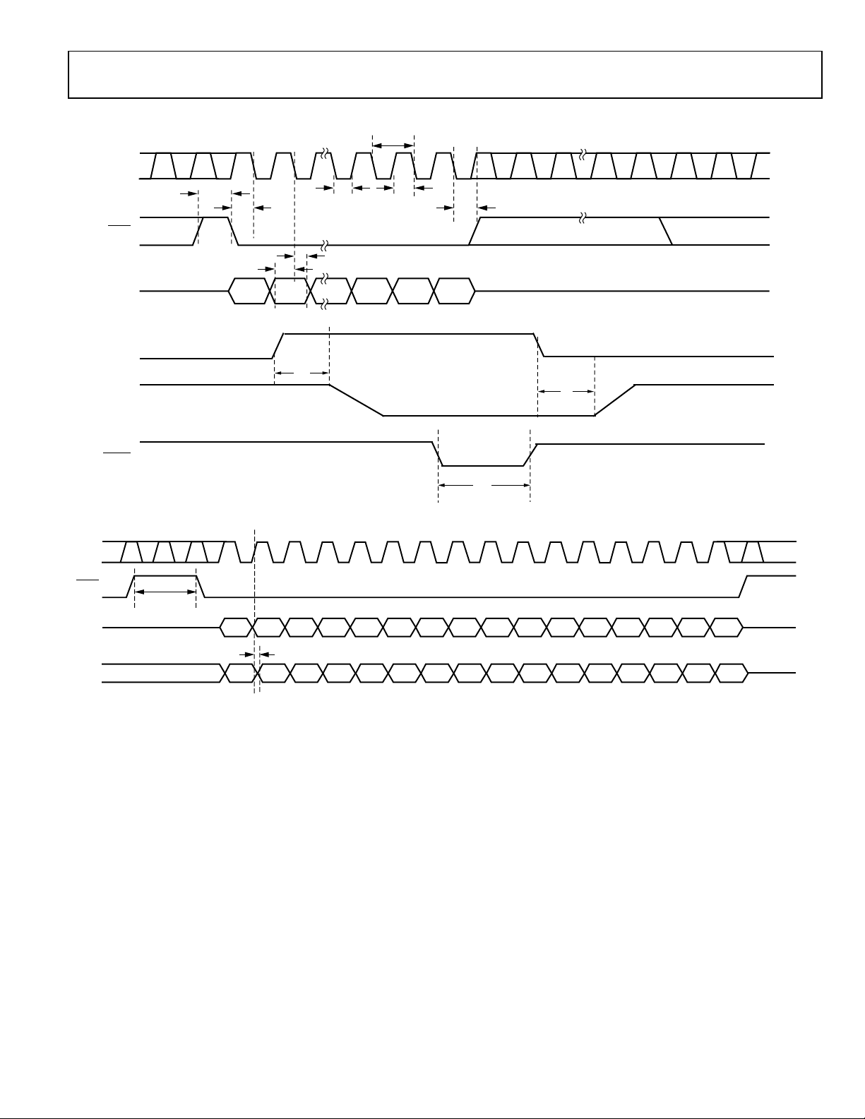
Data Sheet AD5750/AD5750-1/AD5750-2
D15
1 2 16
D0
t
1
t
2
t
5
t
8
t
7
t
3
SCLK
SYNC
SDIN
CLEAR
VOUT
t
10
t
9
t
13
RESET
t
4
t
6
07268-003
t
11
t
12
A2
SDIN
SYNC
SCLK
A0 R = 1 0 R3 R2 R1 R0
CLRSEL OUTEN CLEAR RSET RESET
0 0A1
XSDO X X X R3 R2 R1 R0
CLRSEL OUTEN RSET
PEC
ERROR
OVER
TEMP
IOUT
FAULT
VOUT
FAULT
X
07268-004
Timing Diagrams
Figure 2. Write Mode Timing Diagram
Figure 3. Readback Mode Timing Diagram
Rev. E | Page 9 of 36
Page 10
AD5750/AD5750-1/AD5750-2 Data Sheet
ABSOLUTE MAXIMUM RATINGS
TA = 25°C, unless otherwise noted. Transient currents of up to
100 mA do not cause SCR latch-up.
Table 4.
Parameter Rating
AVDD to GND −0.3 V to +30 V
AVSS to GND +0.3 V to −28 V
AVDD to AVSS −0.3 V to +58 V
DVCC to GND −0.3 V to +7 V
VSENSE+ to GND AVSS to AVDD
VSENSE− to GND ±5.0 V
Digital Inputs to GND
Digital Outputs to GND
VREF to GND −0.3 V to +7 V
VIN to GND −0.3 V to +7 V
VOUT, IOUT to GND AVSS to AVDD
Operating Temperature Range,
Industrial
Storage Temperature Range −65°C to +150°C
Junction Temperature (TJ max) 125°C
32-Lead LFCSP Package
θJA Thermal Impedance 28°C/W
Lead Temperature JEDEC industry standard
Soldering J-STD-020
ESD (Human Body Model) 3 kV
−0.3 V to DV
+7 V (whichever is less)
−0.3 V to DV
+7 V (whichever is less)
−40°C to +105°C
+ 0.3 V or
CC
+ 0.3 V or
CC
Stresses above those listed under Absolute Maximum Ratings
may cause permanent damage to the device. This is a stress
rating only; functional operation of the device at these or any
other conditions above those indicated in the operational
section of this specification is not implied. Exposure to absolute
maximum rating conditions for extended periods may affect
device reliability.
ESD CAUTION
Rev. E | Page 10 of 36
Page 11
Data Sheet AD5750/AD5750-1/AD5750-2
C
2
PIN CONFIGURATION AND FUNCTION DESCRIPTIONS
C
AULT/TEMP
NC/IFAULT
F
RESET
32
31
30
PIN 1
INDICATOR
1SDO/VFAULT
2CLRSEL
AD5750/
3CLEAR
AD5750-1/
4DV
CC
NOTES
1. NC = NO CONNE
. THE EXPOSED PADDLE IS TIED TO AVSS.
5GND
6SYNC/RSET
7SCLK/OUTEN
8SDIN/R0
AD5750-2
TOP VIEW
(Not to Scale)
9
11
10
AD1/R2
AD0/R3
AD2/R1
T.
Figure 4. Pin Configuration
Table 5. Pin Function Descriptions
Pin No. Mnemonic Description
1 SDO/VFAULT
Serial Data Output (SDO). In software mode, this pin is used to clock data from the input shift register in
readback mode. Data is clocked out on the rising edge of SCLK and is valid on the falling edge of SCLK. This pin
is a CMOS output.
Short-Circuit Fault Alert (VFAULT). In hardware mode, this pin acts as a short-circuit fault alert pin and is
asserted low when a short-circuit error is detected. This pin is an open-drain output and must be connected to
a pull-up resistor.
2 CLRSEL
In hardware or software mode, this pin selects the clear value, either zero-scale or midscale code. In software
mode, this pin is implemented as a logic OR with the internal CLRSEL bit.
3 CLEAR
Active High Input. Asserting this pin sets the output current/voltage to zero-scale code or midscale code of the
range selected (user selectable). CLEAR is a logic OR with the internal clear bit.
In software mode, during power-up, the CLEAR pin level determines the power-on condition of the voltage
channel, which can be active 0 V or tristate. See the Asynchronous Clear (CLEAR) section for more details.
4 DVCC Digital Power Supply.
5 GND Ground Connection.
6
/RSET Positive Edge Sensitive Latch (SYNC). In software mode, a rising edge parallel loads the input shift register data
SYNC
into the AD5750/AD5750-1/AD5750-2, also updating the output.
Resistor Select (RSET). In hardware mode, this pin selects whether the internal or the external current sense resistor is
used. If RSET = 0, the external sense resistor is chosen, and if RSET = 1, the internal sense resistor is chosen.
7 SCLK/OUTEN
Serial Clock Input (SCLK). In software mode, data is clocked into the input shift register on the falling edge of
SCLK. This pin operates at clock speeds up to 50 MHz.
Output Enable (OUTEN). In hardware mode, this pin acts as an output enable pin.
8 SDIN/R0 Serial Data Input (SDIN). In software mode, data must be valid on the falling edge of SCLK.
Range Decode Bit (R0). In hardware mode, this pin, in conjunction with R1, R2, and R3, selects the output
current/voltage range setting on the part.
9 AD2/R1
Device Addressing Bit (AD2). In software mode, this pin, in conjunction with AD1 and AD0, allows up to eight
devices to be addressed on one bus.
Range Decode Bit (R1). In hardware mode, this pin, in conjunction with R0, R2, and R3, selects the output
current/voltage range setting on the part.
10 AD1/R2
Device Addressing Bit (AD1). In software mode, this pin, in conjunction with AD2 and AD0, allows up to eight
devices to be addressed on one bus.
Range Decode Bit (R2). In hardware mode, this pin, in conjunction with R0, R1, and R3, selects the output
current/voltage range setting on the part.
C
NC
N
NC
N
HW SELECT
29
28
27
26
25
24 VSENSE+
23 VOUT
22 VSENSE–
21 AV
SS
20 COMP1
19 COMP2
18 IOUT
17 AV
DD
12
15
13
16
14
VIN
GND
VREF
REXT2
REXT1
07268-005
Rev. E | Page 11 of 36
Page 12

AD5750/AD5750-1/AD5750-2 Data Sheet
12, 13
REXT2, REXT1
A 15 kΩ external current setting resistor can be connected between the REXT1 and REXT2 pins to improve the
Pin No. Mnemonic Description
11 AD0/R3 Device Addressing Bit (AD0). In software mode, this pin, in conjunction with AD1 and AD2, allows up to eight
devices to be addressed on one bus.
Range Decode Bit (R3). In hardware mode, this pin, in conjunction with R0, R1, and R2, selects the output
current/voltage range setting on the part.
IOUT temperature drift performance.
14 VREF Buffered Reference Input.
15 VIN Buffered Analog Input (0 V to 4.096 V).
16 GND Ground Connection.
17 AVDD Positive Analog Supply.
18 IOUT Current Output.
19, 20 COMP2,
COMP1
21 AVSS Negative Analog Supply.
22 VSENSE− Sense Connection for the Negative Voltage Output Load Connection. This pin must stay within ±3.0 V of
23 VOUT Buffered Analog Output Voltage.
24 VSENSE+ Sense Connection for the Positive Voltage Output Load Connection.
25, 26,
27, 28
29 HW SELECT This pin is used to configure the part to hardware or software mode. HW SELECT = 0 selects software control,
30
31 FAULT/TEMP Fault Alert (FAULT). In software mode, this pin acts as a general fault alert pin. It is asserted low when an open-
Overtemperature Fault (TEMP). In hardware mode, this pin acts as an overtemperature fault pin. It is asserted
32 N C/ IFA ULT No Connect (NC). In software mode, this pin is a no connect. Instead, tie this pin to GND.
Open-Circuit Fault Alert (IFAULT). In hardware mode, this pin acts as an open-circuit fault alert pin. It is asserted
EPAD The exposed paddle is tied to AVSS.
NC No Connect. Can be tied to GND.
Resets the part to its power-on state.
RESET
Optional Compensation Capacitor Connections for the Voltage Output Buffer. These pins are used to drive
higher capacitive loads on the output. They also reduce overshoot on the output. Care should be taken when
choosing the value of the capacitor connected between the COMP1 and COMP2 pins because it has a direct
influence on the settling time of the output. See the Driving Large Capacitive Loads section for further details.
ground for correct operation.
and HW SELECT = 1 selects hardware control.
circuit error, short-circuit error, overtemperature error, or PEC interface error is detected. This pin is an open-
drain output and must be connected to a pull-up resistor.
low when an overtemperature error is detected. This pin is an open-drain output and must be connected to a
pull-up resistor.
low when an open-circuit error is detected. This pin is an open-drain output and must be connected to a pull-
up resistor.
Rev. E | Page 12 of 36
Page 13

Data Sheet AD5750/AD5750-1/AD5750-2
0.0020
–0.0030
–0.0025
–0.0020
–0.0015
–0.0010
–0.0005
0
0.0005
0.0010
0.0015
0 4.0963.5112.9262.3411.7551.1700.585
INTEGRAL NONLINEARITY ERROR ( %FSR)
V
IN
(V)
+5V
+10V
±5V
±10V
AV
DD
= +24V
AV
SS
= –24V
07268-105
0.005
–0.005
–0.004
–0.003
–0.002
–0.001
0
0.001
0.002
0.003
0.004
10525–40
INTEGRAL NONLINEARITY ERROR ( %FSR)
TEMPERATURE (°C)
AVDD = +24V
AV
SS
= –24V
+5V LINEARITY, NO LOAD
+10V LINEARITY, NO LOAD
±5V LINEARITY, NO LOAD
±10V LINEARITY, NO LOAD
07268-106
0.006
–0.010
–0.008
–0.006
–0.004
–0.002
0.004
0.002
0
0 4.0963.5112.9262.3411.7551.1700.585
TUE (%FSR)
VIN (V)
+5V
+10V
±5V
±10V
AVDD = +24V
AV
SS
= –24V
07268-107
0.10
–0.10
–0.08
–0.06
–0.04
–0.02
0
0.02
0.04
0.06
0.08
10525–40
TUE (%FSR)
TEMPERATURE (°C)
+5V POSITIVE TUE, NO LOAD
+10V POSITIVE TUE, NO LOAD
±5V POSITIVE TUE, NO LOAD
±10V POSITIVE TUE, NO LOAD
+5V NEGATIVE TUE, NO LOAD
+10V NEGATIVE TUE, NO LOAD
±5V NEGATIVE TUE, NO LOAD
±10V NEGATIVE TUE, NO LOAD
07268-108
0.03
–0.04
–0.03
–0.02
–0.01
0
0.01
0.02
10525–40
FULL-S CALE ERROR (%FS R)
TEMPERATURE (°C)
+5V RANGE, F ULL-SCALE E RROR
+10V RANGE, F ULL-SCALE E RROR
±5V RANGE, F ULL-SCALE E RROR
±10V RANGE, F ULL-SCALE E RROR
07268-109
2.5
–2.5
–2.0
–1.5
–1.0
–0.5
0
0.5
1.0
1.5
2.0
10525–40
BIPOLAR ZERO ERROR (mV )
TEMPERATURE (°C)
±5V ZERO ERROR
±10V ZERO ERROR
AVDD = +24V
AV
SS
= –24V
07268-110
TYPICAL PERFORMANCE CHARACTERISTICS
VOLTAGE OUTPUT
Figure 5. Integral Nonlinearity Error vs. V
IN
Figure 6. Integral Nonlinearity Error vs. Temperature
Figure 8. Total Unadjusted Error (TUE) vs. Temperature
Figure 9. Full-Scale Error vs. Temperature
Figure 7. Total Unadjusted Error (TUE) vs. V
IN
Figure 10. Bipolar Zero Error vs. Temperature
Rev. E | Page 13 of 36
Page 14

AD5750/AD5750-1/AD5750-2 Data Sheet
0.020
–0.025
–0.020
–0.015
–0.010
–0.005
0
0.005
0.010
0.015
10525–40
GAIN ERROR ( %FSR)
TEMPERATURE (°C)
AV
DD
= +24V
AV
SS
= –24V
+5V GAIN, NO LOAD
+10V GAIN, NO LOAD
±5V GAIN, NO LOAD
±10V GAIN, NO LOAD
07268-111
2.5
–3.0
–2.5
–2.0
–1.5
–1.0
–0.5
0
0.5
1.5
2.0
1.0
10525–40
ZERO-SCALE ERROR (mV)
TEMPERATURE (°C)
AV
DD
= +24V
AV
SS
= –24V
OUTPUT UNLOADED
+5V RANGE
+10V RANGE
±5V RANGE
±10V RANGE
07268-112
0.003
–0.003
–0.002
–0.001
0
0.001
0.002
INTEGRAL NONLINEARITY ERROR ( %FSR)
SUPPLY VOLTAGES (AVDD/AVSS)
+11.2/–10.8 ±15.0 ±24.0 ±26.4
+5V LINEARITY, NO LOAD
+10V LINEARITY, NO LOAD
±5V LINEARITY, NO LOAD
±10V LINEARITY, NO LOAD
07268-113
0.10
–0.10
–0.08
–0.06
–0.04
–0.02
0
0.02
0.04
0.06
0.08
TUE (%FSR)
SUPPLY VOLTAGES (AV
DD
/AV
SS
)
+11.2/–10.8 ±15.0 ±24.0 ±26.4
+5V POSITIVE TUE, NO LOAD
+10V POSITIVE TUE, NO LOAD
±5V POSITIVE TUE, NO LOAD
±10V POSITIVE TUE, NO LOAD
+5V NEGATIVE TUE, NO LOAD
+10V NEGATIVE TUE, NO LOAD
±5V NEGATIVE TUE, NO LOAD
±10V NEGATIVE TUE, NO LOAD
07268-114
1.2
1.0
0.8
0.6
0.4
0.2
0
10525–40
HEADROOM (V )
TEMPERATURE (°C)
±10V VDD HEADROOM, LOAD OFF
07268-115
0.05
–0.05
–0.04
–0.03
–0.02
–0.01
0
0.01
0.02
0.03
0.04
15–15 –13 –11 –9 –7 –5 –3 –1 1 3 5 7 9 11 13
OUTPUT VOLTAGE DELTA (V)
SOURCE/SINK CURRENT (mA)
+5V RANGE
±10V RANGE
07268-116
Figure 11. Gain Error vs. Temperature
Figure 12. Zero-Scale Error (Offset Error) vs. Temperature
Figure 14. Total Unadjusted Error (TUE) vs. Supply Voltages
Figure 15. AVDD Headroom, ±10 V Range, Output Set to 10 V, Load Off
Figure 13. Integral Nonlinearity Error vs. Supply Voltage
Figure 16. Source and Sink Capability of Output Amplifier
Rev. E | Page 14 of 36
Page 15

Data Sheet AD5750/AD5750-1/AD5750-2
12
10
8
6
4
2
0
2722171272–3–8
VOLTAGE (V)
TIME (µs)
07268-117
12
10
8
6
4
2
0
2722171272–3–8
VOLTAGE (V)
TIME (µs)
07268-118
40
35
30
25
20
15
10
5
0
–5
2.52.01.51.00.50–0.5–1.0
V
OUT
(mV)
TIME (ms)
07268-119
CH1 5.00V CH2 20.0mV
B
W
M1.0µs A CH1 3.00V
1
2
07268-120
5µV/DIV 1s/DIV
07268-121
100µV/DIV
1s/DIV
07268-122
Figure 17. Full-Scale Positive Step
Figure 18. Full-Scale Negative Step
Figure 20. V
Enable Glitch, Load = 2 kΩ || 1 nF
OUT
Figure 21. Peak-to-Peak Noise (0.1 Hz to 10 Hz Bandwidth)
Figure 19. V
vs. Time on Power-Up, Load = 2 kΩ || 200 pF
OUT
Figure 22. Peak-to-Peak Noise (100 kHz Bandwidth)
Rev. E | Page 15 of 36
Page 16

AD5750/AD5750-1/AD5750-2 Data Sheet
4.0
3.5
3.0
2.5
2.0
1.5
1.0
0.5
0
1.0
0.8
0.6
0.4
0.2
0
–0.2
2.01.5
V
DD
V
OUT
1.00.50–0.5–1.0–1.5
V
DD
(V)
V
OUT
(V)
TIME (ms)
07268-123
Figure 23. VDD and V
vs. Time on Power-Up
OUT
Rev. E | Page 16 of 36
Page 17

Data Sheet AD5750/AD5750-1/AD5750-2
0.004
–0.010
–0.008
–0.006
–0.004
–0.002
0.002
0
0 4.0963.5112.9262.3411.7551.1700.585
INTEGRAL NONLINEARITY ERROR ( %FSR)
V
IN
(V)
AV
DD
= +24V
AV
SS
= –24V
+4mA TO +20mA
0mA TO +20mA
0mA TO +24mA
±20mA
±24mA
07268-124
0.004
–0.012
–0.010
–0.008
–0.006
–0.004
–0.002
0.002
0
0 4.0963.5112.9262.3411.7551.1700.585
INTEGRAL NONLINEARITY ERROR ( %FSR)
V
IN
(V)
AV
DD
= +24V
AV
SS
= –24V
+4mA TO +20mA
0mA TO +20mA
0mA TO +24mA
±20mA
±24mA
07268-125
0.010
–0.010
–0.008
–0.006
–0.004
–0.002
0
0.002
0.004
0.006
0.008
INTEGRAL NONLINEARITY ERROR ( %FSR)
SUPPLY VOLTAGES (AVDD/AV
SS
)
+11.2/–10.8 ±15.0 ±24.0 ±26.4
+4mA TO +20mA EXTERNAL R
SET
LINEARITY
0mA TO +20mA EXT E RNAL R
SET
LINEARITY
0mA TO +24mA EXT E RNAL R
SET
LINEARITY
±20mA EXTERNAL R
SET
LINEARITY
±24mA EXTERNAL R
SET
LINEARITY
07268-126
0.010
–0.010
–0.008
–0.006
–0.004
–0.002
0
0.002
0.004
0.006
0.008
INTEGRAL NONLINEARITY ERROR ( %FSR)
SUPPLY VOLTAGES (AVDD/AV
SS
)
+11.2/–10.8 ±15.0 ±24.0 ±26.4
+4mA TO +20mA INTERNAL R
SET
LINEARITY
0mA TO +20mA INT E RNAL R
SET
LINEARITY
0mA TO +24mA INT E RNAL R
SET
LINEARITY
±20mA INTERNAL R
SET
LINEARITY
±24mA INTERNAL R
SET
LINEARITY
07268-127
0.010
–0.008
–0.006
–0.004
–0.002
0
0.002
0.004
0.006
0.008
0 4.0963.5112.9262.3411.7551.1700.585
TUE (%FSR)
VIN (V)
AV
DD
= +24V
AV
SS
= –24V
+4mA TO +20mA
0mA TO +20mA
0mA TO +24mA
±20mA
±24mA
07268-128
0.015
–0.015
–0.010
–0.005
0
0.005
0.010
0 4.0963.5112.9262.3411.7551.1700.585
TUE (%FSR)
VIN (V)
AV
DD
= +24V
AV
SS
= –24V
+4mA TO +20mA
0mA TO +20mA
0mA TO +24mA
±20mA
±24mA
07268-129
CURRENT OUTPUT
Figure 24. Integral Nonlinearity Error vs. VIN, External R
Figure 25. Integral Nonlinearity Error vs. VIN, Internal R
Resistor
SET
Resistor
SET
Figure 27. Integral Nonlinearity Error, Current Mode,
Internal R
Sense Resistor
SET
Figure 28. Total Unadjusted Error (TUE) vs. VIN, External R
Resistor
SET
Figure 26. Integral Nonlinearity Error, Current Mode,
External R
Sense Resistor
SET
Figure 29. Total Unadjusted Error vs. VIN, Internal R
Resistor
SET
Rev. E | Page 17 of 36
Page 18

AD5750/AD5750-1/AD5750-2 Data Sheet
0.10
–0.10
–0.08
–0.06
–0.04
–0.02
0
0.02
0.04
0.06
0.08
TUE (%FSR)
SUPPLY VOLTAGES (AV
DD
/AV
SS
)
+11.2/–10.8 ±15.0 ±24.0 ±26.4
+4mA TO +20mA EXTERNAL R
SET
POSITIVE TUE
0mA TO +20mA EXT E RNAL R
SET
POSITIVE TUE
0mA TO +24mA EXT E RNAL R
SET
POSITIVE TUE
±20mA EXTERNAL R
SET
POSITIVE TUE
±24mA EXTERNAL R
SET
POSITIVE TUE
+4mA TO +20mA EXTERNAL R
SET
NEGATIVE TUE
0mA TO +20mA EXT E RNAL R
SET
NEGATIVE TUE
0mA TO +24mA EXT E RNAL R
SET
NEGATIVE TUE
±20mA EXTERNAL R
SET
NEGATIVE TUE
±24mA EXTERNAL R
SET
NEGATIVE TUE
07268-130
0.10
–0.10
–0.08
–0.06
–0.04
–0.02
0
0.02
0.04
0.06
0.08
TUE (%FSR)
SUPPLY VOLTAGES (AVDD/AV
SS
)
+11.2/–10.8 ±15.0 ±24.0 ±26.4
+4mA TO +20mA INTERNAL R
SET
POSITIVE TUE
0mA TO +20mA INT E RNAL R
SET
POSITIVE TUE
0mA TO +24mA INT E RNAL R
SET
POSITIVE TUE
±20mA INTERNAL R
SET
POSITIVE TUE
±24mA INTERNAL R
SET
POSITIVE TUE
+4mA TO +20mA INTERNAL R
SET
NEGATIVE TUE
0mA TO +20mA INT E RNAL R
SET
NEGATIVE TUE
0mA TO +24mA INT E RNAL R
SET
NEGATIVE TUE
±20mA INTERNAL R
SET
NEGATIVE TUE
±24mA INTERNAL R
SET
NEGATIVE TUE
07268-131
10525–40
TEMPERATURE (°C)
0.010
–0.010
–0.008
–0.006
–0.004
–0.002
0
0.002
0.004
0.006
0.008
LINEARITY (%FSR)
+4mA TO +20mA INTERNAL R
SET
LINEARITY
0mA TO +20mA INT E RNAL R
SET
LINEARITY
0mA TO +24mA INT E RNAL R
SET
LINEARITY
±20mA INTERNAL R
SET
LINEARITY
±24mA INTERNAL R
SET
LINEARITY
AVDD = +24V
AV
SS
= –24V
07268-132
10525–40
TEMPERATURE (°C)
0.010
–0.010
–0.008
–0.006
–0.004
–0.002
0
0.002
0.004
0.006
0.008
LINEARITY (%FSR)
+4mA TO +20mA EXTERNAL R
SET
LINEARITY
0mA TO +20mA EXT E RNAL R
SET
LINEARITY
0mA TO +24mA EXT E RNAL R
SET
LINEARITY
±20mA EXTERNAL R
SET
LINEARITY
±24mA EXTERNAL R
SET
LINEARITY
AV
DD
= +24V
AV
SS
= –24V
07268-133
10525–40
TEMPERATURE (°C)
0.10
–0.10
–0.08
–0.06
–0.04
–0.02
0
0.02
0.04
0.06
0.08
TUE (%FSR)
+4mA TO +20mA INT ERNAL R
SET
POSITIVE TUE
0mA TO + 2 0mA INTERNAL R
SET
POSITIVE TUE
0mA TO + 2 4mA INTERNAL R
SET
POSITIVE TUE
±20mA INT ERNAL R
SET
POSITIVE TUE
±24mA INT ERNAL R
SET
POSITIVE TUE
+4mA TO +20mA INT ERNAL R
SET
NEGATIVE TUE
0mA TO + 2 0mA INTERNAL R
SET
NEGATIVE TUE
0mA TO + 2 4mA INTERNAL R
SET
NEGATIVE TUE
±20mA INT ERNAL R
SET
NEGATIVE TUE
±24mA INT ERNAL R
SET
NEGATIVE TUE
07268-134
0.10
–0.10
–0.08
–0.06
–0.04
–0.02
0
0.02
0.04
0.06
0.08
TUE (%FSR)
+4mA TO +20mA EXTERNAL R
SET
POSITIVE TUE
0mA TO + 2 0mA EXTERNAL R
SET
POSITIVE TUE
0mA TO + 2 4mA EXTERNAL R
SET
POSITIVE TUE
±20mA EXTERNAL R
SET
POSITIVE TUE
±24mA EXTERNAL R
SET
POSITIVE TUE
+4mA TO +20mA EXTERNAL R
SET
NEGATIVE TUE
0mA TO + 2 0mA EXTERNAL R
SET
NEGATIVE TUE
0mA TO + 2 4mA EXTERNAL R
SET
NEGATIVE TUE
±20mA EXTERNAL R
SET
NEGATIVE TUE
±24mA EXTERNAL R
SET
NEGATIVE TUE
10525–40
TEMPERATURE (°C)
07268-135
Figure 30. Total Unadjusted Error (TUE), Current Mode,
External R
Sense Resistor
SET
Figure 31. Total Unadjusted Error (TUE), Current Mode,
Internal R
Sense Resistor
SET
Figure 33. INL vs. Temperature, External R
Sense Resistor
SET
Figure 34. Total Unadjusted Error (TUE) vs. Temperature,
Internal R
Sense Resistor
SET
Figure 32. INL vs. Temperature, Internal R
Sense Resistor
SET
Figure 35. Total Unadjusted Error (TUE) vs. Temperature,
External R
Sense Resistor
SET
Rev. E | Page 18 of 36
Page 19

Data Sheet AD5750/AD5750-1/AD5750-2
6
–6
–4
–2
0
2
4
ZERO-SCALE ERROR (µA)
10525–40
TEMPERATURE (°C)
AVDD = +24V
AV
SS
= –24V
+4mA TO +20mA EXTERNAL R
SET
0mA TO +20mA EXT E RNAL R
SET
0mA TO +24mA EXT E RNAL R
SET
±20mA EXTERNAL R
SET
±24mA EXTERNAL R
SET
07268-136
25
–20
–15
–10
–5
0
5
10
15
20
ZERO-SCALE ERROR (µA)
10525–40
TEMPERATURE (°C)
AV
DD
= +24V
AV
SS
= –24V
+4mA TO +20mA INTERNAL R
SET
0mA TO +20mA INT E RNAL R
SET
0mA TO +24mA INT E RNAL R
SET
±20mA INTERNAL R
SET
±24mA INTERNAL R
SET
07268-137
3
–5
–4
–3
–2
–1
0
1
2
BIPOLAR ZERO-SCALE E RROR (µA)
10525–40
TEMPERATURE (°C)
AV
DD
= +24V
AV
SS
= –24V
±20mA, EXTERNAL R
SET
±24mA, EXTERNAL R
SET
07268-138
2
–6
–5
–4
–3
–2
–1
0
1
BIPOLAR ZERO-SCALE E RROR (µA)
10525–40
TEMPERATURE (°C)
AV
DD
= +24V
AV
SS
= –24V
±20mA, INTERNAL R
SET
±24mA, INTERNAL R
SET
07268-139
0.04
–0.04
–0.03
–0.02
–0.01
0
0.01
0.02
0.03
FULL-S CALE ERROR (%FS R)
10525–40
TEMPERATURE (°C)
AV
DD
= +24V
AV
SS
= –24V
+4mA TO +20mA EXTERNAL R
SET
0mA TO +20mA EXT E RNAL R
SET
0mA TO +24mA EXT E RNAL R
SET
±20mA EXTERNAL R
SET
±24mA EXTERNAL R
SET
07268-140
0.04
–0.06
–0.04
–0.05
–0.03
–0.02
–0.01
0
0.01
0.02
0.03
FULL-S CALE ERROR (%FS R)
10525–40
TEMPERATURE (°C)
AVDD = +24V
AV
SS
= –24V
+4mA TO +20mA INTERNAL R
SET
0mA TO +20mA INT E RNAL R
SET
0mA TO +24mA INT E RNAL R
SET
±20mA INTERNAL R
SET
±24mA INTERNAL R
SET
07268-141
Figure 36. Zero-Scale Error vs. Temperature, External R
Figure 37. Zero-Scale Error vs. Temperature, Internal R
Sense Resistor
SET
Sense Resistor
SET
Figure 39. Bipolar Zero-Scale Error vs. T emperature,
Internal R
Sense Resistor
SET
Figure 40. Full-Scale Error vs. Temperature, External R
Sense Resistor
SET
Figure 38. Bipolar Zero-Scale Error vs. T emperature,
External R
SET
Sense Resistor
Figure 41. Full-Scale Error vs. Temperature, Internal R
Sense Resistor
SET
Rev. E | Page 19 of 36
Page 20

AD5750/AD5750-1/AD5750-2 Data Sheet
0.020
0.015
–0.015
–0.010
–0.005
0
0.005
0.010
GAIN ERROR ( %FSR)
10525–40
TEMPERATURE (°C)
AVDD = +24V
AV
SS
= –24V
+4mA TO +20mA EXTERNAL R
SET
0mA TO +20mA EXT E RNAL R
SET
0mA TO +24mA EXT E RNAL R
SET
±20mA EXTERNAL R
SET
±24mA EXTERNAL R
SET
07268-142
0.08
–0.10
–0.08
–0.06
–0.04
–0.02
0
0.04
0.02
0.06
GAIN ERROR ( %FSR)
10525–40
TEMPERATURE (°C)
AVDD = +24V
AV
SS
= –24V
+4mA TO +20mA INTERNAL R
SET
0mA TO +20mA INT E RNAL R
SET
0mA TO +24mA INT E RNAL R
SET
±20mA INTERNAL R
SET
±24mA INTERNAL R
SET
07268-143
1.4
1.2
1.0
0.8
0.6
0.4
0.2
0
COMPLIANCE (V)
10525–40
TEMPERATURE (°C)
AV
DD
COMPLI ANCE
AV
SS
COMPLI ANCE
07268-144
12
10
8
6
4
2
0
–2
0.000010
–0.000010
–0.000008
–0.000006
–0.000004
–0.000002
0
0.000002
0.000004
0.000006
0.000008
10
V
DD
I
OUT
–10 –8 –6 –4 –2 0 2 4 6 8
V
DD
(V)
I
OUT
(A)
TIME (ms)
07268-145
0
–18
–16
–14
–12
–10
–8
–6
–4
–2
8–2 –1 0 1 2 3 4 5 6 7
I
OUT
(V)
TIME (µs)
07268-146
0.025
0.020
0.015
0.010
0.005
0
68615448413428211481–12 –6
CURRENT (A)
TIME (µs)
07268-147
Figure 42. Gain Error vs. Temperature, External R
Figure 43. Gain Error vs. Temperature, Internal R
Sense Resistor
SET
Sense Resistor
SET
Figure 45. V
and Output Current (I
DD
) vs. Time-On Power-Up
OUT
Figure 46. Output Current (I
) vs. Time-On Output Enable
OUT
Tested When I
Figure 44. Output Compliance vs. Temperature
= 10.8 mA, ±24 mA Range Selected
OUT
Rev. E | Page 20 of 36
Figure 47. 4 mA to 20 mA Output Current Step
Page 21

Data Sheet AD5750/AD5750-1/AD5750-2
3000
2500
2000
1500
1000
500
0
0 0.5 1.0 1.5 2.0 2.5 3.0 3.5 4.0 4.5 5.0
DI
CC
(µA)
LOGIC LEVEL (V)
DV
CC
= 5V
DV
CC
= 3V
07268-148
6
5
4
3
2
1
0
–1
–2
–3
AI
DD
/AI
SS
(mA)
AV
DD
/AVSS (V)
±10.8 ±15.0 ±24.0 ±26.4
AI
DD
AI
SS
07268-149
6
5
4
3
2
1
0
–1
–2
–3
AI
DD
/AI
SS
(mA)
AV
DD
/AVSS (V)
±10.8 ±15.0 ±24.0 ±26.4
AI
DD
AI
SS
07268-150
Figure 48. DICC vs. Logic Input Voltage
Figure 50. AIDD/AISS vs. AVDD/AVSS, I
OUT
= 0 mA
Figure 49. AIDD/AISS vs. AVDD/AVSS, V
OUT
= 0 V
Rev. E | Page 21 of 36
Page 22

AD5750/AD5750-1/AD5750-2 Data Sheet
TERMINOLOGY
Total Unadjusted Error (TUE)
TUE is a measure of the output error taking all the various
errors into account: INL error, offset error, gain error, and
output drift over supplies, temperature, and time. TUE is
expressed as a percentage of full-scale range (% FSR).
Relative Accuracy or Integral Nonlinearity (INL)
INL is a measure of the maximum deviation, in % FSR, from a
straight line passing through the endpoints of the output driver
transfer function. A typical INL vs. input voltage plot can be
seen in Figure 5.
Bipolar Zero Error
Bipolar zero error is the deviation of the actual vs. ideal half-scale
output of 0 V/0 mA with a bipolar range selected. A plot of
bipolar zero error vs. temperature can be seen in Figure 10.
Bipolar Zero Temperature Coefficient (TC)
Bipolar zero TC is a measure of the change in the bipolar zero error
with a change in temperature. It is expressed in ppm FSR/°C.
Full-Scale Error
Full-scale error is the deviation of the actual full-scale analog
output from the ideal full-scale output. Full-scale error is
expressed as a percentage of full-scale range (% FSR).
Full-Scale Temperature Coefficient (TC)
Full-scale TC is a measure of the change in the full-scale error
with a change in temperature. It is expressed in ppm FSR/°C.
Gain Error
Gain error is a measure of the span error of the output. It is the
deviation in slope of the output transfer characteristic from the
ideal expressed in % FSR. A plot of gain error vs. temperature
can be seen in Figure 11.
Gain Error Temperature Coefficient (TC)
Gain error TC is a measure of the change in gain error with
changes in temperature. Gain error TC is expressed in ppm
FSR/°C.
Zero-Scale Error
Zero-scale error is the deviation of the actual zero-scale analog
output from the ideal zero-scale output. Zero-scale error is
expressed in millivolts (mV).
Zero-Scale TC
Zero-scale TC is a measure of the change in zero-scale error
with a change in temperature. Zero-scale error TC is expressed
in ppm FSR/°C.
Offset Error
Offset error is a measurement of the difference between the
actual VOUT and the ideal VOUT, expressed in millivolts (mV)
in the linear region of the transfer function. It can be negative
or positive.
Output Voltage Settling Time
Output voltage settling time is the amount of time it takes for
the output to settle to a specified level for a half-scale input change.
Slew Rate
The slew rate of a device is a limitation in the rate of change of the
output voltage. The output slewing speed is usually limited by the
slew rate of the amplifier used at its output. Slew rate is measured
from 10% to 90% of the output signal and is expressed in V/µs.
Current Loop Voltage Compliance
Current loop voltage compliance is the maximum voltage at
the IOUT pin for which the output current is equal to the
programmed value.
Power-On Glitch Energy
Power-on glitch energy is the impulse injected into the analog
output when the AD5750/AD5750-1/AD5750-2 are powered on.
It is specified as the area of the glitch in nV-sec.
Power Supply Rejection Ratio (PSRR)
PSRR indicates how the output is affected by changes in the
power supply voltage.
Rev. E | Page 22 of 36
Page 23

Data Sheet AD5750/AD5750-1/AD5750-2
07268-045
VSENSE+
VSENSE–
VIN
SCLK
VDD
REFIN
SDI/DIN
SDO
SYNC1
SYNC
SDO
SDIN
SCLK
AD506x
AD566x
MCU
VOUT
0V TO +5V, 0V TO +10V,
±5V, ±10V
IOUT
0mA TO +20mA,
0mA TO +24mA,
+4mA TO +20mA
±20mA, ±24mA
VOUT
RANGE
SCALE
IOUT
RANGE
SCALE
VOUT SHO RT FAULT
IOUT OPENFAULT
OVERTEMP FAULT
STATUS REGISTER
SERIAL
INTERFACE
VREF
HW SELECT
FAULT
ADP1720
ADR392
VDD AGND VSS
AV
DD
GND AV
SS
AD5750/
AD5750-1/
AD5750-2
THEORY OF OPERATION
The AD5750/AD5750-1/AD5750-2 are single-channel, precision
voltage/current output drivers with hardware- or softwareprogrammable output ranges. The software ranges are configured
via an SPI-/MICROWIRE-compatible serial interface. The analog
input to the AD5750/AD5750-1/AD5750-2 is provided from a
low voltage, single-supply DAC and is internally conditioned to
provide the desired output current/voltage range. Analog input
ranges available are 0 V to 2.5 V (AD5750-1/AD5750-2) or 0 V
to 4.096 V (AD5750).
The output current range is programmable across five current
ranges: +4 mA to +20 mA, 0 mA to +20 mA, 0 mA to +24 mA,
±20 mA, and ±24 mA.
The voltage output is provided from a separate pin that can be
configured to provide 0 V to +5 V, 0 V to +10 V, ±5 V, or ±10 V
output ranges. An overrange of 20% is available on the voltage
ranges. An overrange of 2% is available on the 4 mA to 20 mA,
0 mA to 20 mA, and 0 mA to 24 mA current ranges. The current
and voltage outputs are available on separate pins. Only one
output can be enabled at one time. The output range is selected
by programming the R3 to R0 bits in the control register (see
Table 7 and Ta b l e 8).
Figure 51 and Figure 52 show a typical configuration of the
AD5750/AD5750-1/AD5750-2 in software mode and in hardware
mode, respectively, in an output module system. The HW SELECT
pin selects whether the part is configured in software or hardware
mode. The analog input to the AD5750/AD5750-1/AD5750-2 is
provided from a low voltage, single-supply DAC, such as the
AD506x or AD566x, which provides an output range of 0 V to
4.096 V. The supply and reference for the DAC, as well as the
reference for the AD5750/AD5750-1/AD5750-2, can be supplied
from a reference such as the ADR392. The AD5750/AD5750-1/
AD5750-2 can operate from supplies up to ±26.4 V.
SOFTWARE MODE
In current mode, software-selectable output ranges include
±20 mA, ±24 mA, 0 mA to +20 mA, +4 mA to +20 mA, and
0 mA to +24 mA.
In voltage mode, software-selectable output ranges include 0 V
to +5 V, 0 V to +10 V, ±5 V, and ±10 V.
Figure 51. Typical System Configuration in Software Mode (Pull-Up Resistors Not Shown for Open-Drain Outputs)
Rev. E | Page 23 of 36
Page 24

AD5750/AD5750-1/AD5750-2 Data Sheet
07268-046
VSENSE+
VSENSE–
R3
R2
R1
R0
OUTPUT RANGE
SELECT PINS
VIN
SCLK
VDD REFIN
SDI/DIN
SDO
SYNC1
AD506x
AD566x
MCU
VOUT
0V TO +5V, 0V TO +10V,
±5V, ±10V
IOUT
0mA TO +20mA,
0mA TO +24mA,
+4mA TO +20mA
±20mA, ±24mA
VOUT
RANGE
SCALE
IOUT
RANGE
SCALE
VREF
TEMP VFAULT IFAULT
ADP1720
ADR392
VDD AGND VSS
OUTEN
HW SELECT
DV
CC
AVDDGND AV
SS
AD5750/
AD5750-1/
AD5750-2
Figure 52. Typical System Configuration in Hardware Mode Using Internal DAC Reference (Pull-Up Resistors Not Shown for Open-Drain Outputs)
Table 6. Suggested Parts for Use with AD5750, AD5750-1, and AD5750-2
DAC Reference Power Accuracy Description
AD5660 Internal ADP17201 12-bit INL Midend system, single channel, internal reference
AD5664R Internal Not applicable Not applicable Midend system, quad channel, internal reference
AD5668 Internal Not applicable Not applicable Midend system, octal channel, internal reference
AD5060 ADR434 ADP17201 16-bit INL High end system, single channel, external reference
AD5064 ADR434 Not applicable Not applicable High end system, quad channel, external reference
AD5662 ADR3922 ADR3922 12-bit INL Midend system, single channel, external reference
AD5664 ADR3922 Not applicable Not applicable Midend system, quad channel, external reference
1
The input range of the ADP1720 is up to 28 V.
2
The input range of the ADR392 is up to 15 V.
Rev. E | Page 24 of 36
Page 25

IOUT
RANGE
SCALING
REXT1
IOUT
R
SET
Vx
V
SS
V
DD
R1 R4
R2 R3
REXT2
IOUT
OPEN FAULT
VIN
VREF
RANGE DECODE
FROM INT E RFACE
07268-047
VOUT RANGE
SCALING
VSENSE+
VOUT
VSENSE–
VOUT
SHORT FAUL T
RANGE DECODE
FROM INT E RFACE
VIN
(0V TO 4.096V )
VREF
07268-048
Data Sheet AD5750/AD5750-1/AD5750-2
CURRENT OUTPUT ARCHITECTURE
The voltage input from the analog input VIN pin (0 V to 4.096 V
for AD5750 and 0 V to 2.5 V for the AD5750-1/AD5750-2) is
either converted to a current (see Figure 53), which is then
mirrored to the supply rail so that the application simply sees
a current source output with respect to an internal reference
voltage, or it is buffered and scaled to output a software-selectable
unipolar or bipolar voltage range (see Figure 54). The reference
is used to provide internal offsets for range and gain scaling.
The selectable output range is programmable through the
digital interface.
Figure 53. Current Output Configuration
Figure 54. Voltage Output
DRIVING INDUCTIVE LOADS
When driving inductive or poorly defined loads, connect a 0.01 µF
capacitor between IOUT and GND. This ensures stability with
loads beyond 50 mH. There is no maximum capacitance limit.
The capacitive component of the load may cause slower settling.
Voltage Output Amplifier
The voltage output amplifier is capable of generating both unipolar
and bipolar output voltages. It is capable of driving a load of 1 kΩ
in parallel with 1.2 µF (with an external compensation capacitor
on the COMP1 and COMP2 pins). The source and sink capabilities
of the output amplifier can be seen in Figure 16. The slew rate
is 2 V/µs.
Internal to the device, there is a 2.5 MΩ resistor connected
between the VOUT and VSENSE+ pins and, similarly, between
the VSENSE− pin and the internal device ground. If a fault
condition occurs, these resistors act to protect the AD5750/
AD5750-1/AD5750-2 by ensuring that the amplifier loop is closed
so that the part does not enter into an open-loop condition.
The VSENSE− pin can work in a common-mode range of ±3 V
with respect to the remote load ground point.
Rev. E | Page 25 of 36
The current and voltage are output on separate pins and cannot
be output simultaneously. This allows the user to tie both the
current and voltage output pins together and configure the end
system as a single channel output.
Driving Large Capacitive Loads
The voltage output amplifier is capable of driving capacitive loads
of up to 1 µF with the addition of a nonpolarized compensation
capacitor between the COMP1 and COMP2 pins.
Without the compensation capacitor, up to 20 nF capacitive loads
can be driven. Care should be taken to choose an appropriate
value for the C
capacitor. This capacitor, while allowing the
COMP
AD5750/AD5750-1/AD5750-2 to drive higher capacitive loads
and reduce overshoot, increases the settling time of the part
and, therefore, affects the bandwidth of the system. Considered
values of this capacitor should be in the range 100 pF to 4 nF,
depending on the trade-off required between settling time,
overshoot, and bandwidth.
POWER-ON STATE OF AD5750/AD5750-1/AD5750-2
On power-up, the AD5750/AD5750-1/AD5750-2 sense whether
hardware or software mode is loaded and set the power-up
conditions accordingly.
In software SPI mode, the power-up state of the output is
dependent on the state of the CLEAR pin. If the CLEAR pin is
pulled high, the part powers up, driving an active 0 V on the
output. If the CLEAR pin is pulled low, the part powers up with
the voltage output channel in tristate mode. In both cases, the
current output channel powers up in the tristate condition (0 mA).
This allows the voltage and current outputs to be connected
together, if desired.
To put the part into normal operation, the user must set the
OUTEN bit in the control register to enable the output and, in
the same write, set the output range configuration using the R3
to R0 range bits. If the CLEAR pin is still high (active) during
this write, the part automatically clears to its normal clear state
as defined by the programmed range and by the CLRSEL pin or
the CLRSEL bit (see the Asynchronous Clear (CLEAR) section
for more details). To operate the part in normal mode, take the
CLEAR pin low.
The CLEAR pin is typically driven directly from a microcontroller.
In cases where the power supply for the AD5750/AD5750-1/
AD5750-2 supply may be independent of the microcontroller
power supply, connect a weak pull-up resistor to DV
down resistor to ground to ensure that the correct power-up
condition is achieved independent of the microcontroller. A
10 kΩ pull-up/pull-down resistor on the CLEAR pin should be
sufficient for most applications.
If hardware mode is selected, the part powers up to the conditions
defined by the R3 to R0 range bits and the status of the OUTEN
or CLEAR pin. It is recommended to keep the output disabled
when powering up the part in hardware mode.
or a pull-
CC
Page 26

AD5750/AD5750-1/AD5750-2 Data Sheet
A2, A1, A0
Used in association with the AD2, AD1, and AD0 external pins to determine which part is being addressed by the system
0 0 1
Addresses part with Pin AD2 = 0, Pin AD1 = 0, Pin AD0 = 1.
1 0 0
Addresses part with Pin AD2 = 1, Pin AD1 = 0, Pin AD0 = 0.
DEFAULT REGISTERS AT POWER-ON
The AD5750/AD5750-1/AD5750-2 power-on-reset circuit
ensures that all registers are loaded with zero code.
In software SPI mode, the part powers up with all outputs
disabled (OUTEN bit = 0). The user must set the OUTEN bit in
the control register to enable the output and, in the same write,
to set the output range configuration using the R3 to R0 bits.
If hardware mode is selected, the part powers up to the
conditions defined by the R3 to R0 bits and the status of the
OUTEN pin. It is recommended to keep the output disabled
when powering up the part in hardware mode.
RESET FUNCTION
In software mode, the part can be reset using the
(active low) or the reset bit (reset = 1). A reset disables both the
current and voltage outputs to their power-on condition. The
user must write to the OUTEN bit to enable the output and, in
the same write, to set the output range configuration. The
pin is a level-sensitive input; the part stays in reset mode as long
RESET
as the
pin is low. The reset bit clears to 0 following a
reset command to the control register.
In hardware mode, there is no reset. If using the part in hardware
mode, tie the
RESET
pin high.
RESET
pin
RESET
OUTEN
In software mode, the output can be enabled or disabled using
the OUTEN bit in the control register. When the output is
disabled, both the current and voltage channels go into tristate.
The user must set the OUTEN bit to enable the output and
simultaneously set the output range configuration.
In hardware mode, the output can be enabled or disabled using
the OUTEN pin. When the output is disabled, both the current
and voltage channels go into tristate. The user must write to the
OUTEN pin to enable the output. It is recommended that the
output be disabled when changing the ranges.
SOFTWARE CONTROL
Software control is enabled by connecting the HW SELECT pin
to ground. In software mode, the AD5750/AD5750-1/AD5750-2
are controlled over a versatile 3-wire serial interface that operates at
clock rates up to 50 MHz. It is compatible with SPI, QSPI™,
MICROWIRE, and DSP standards.
Input Shift Register
The input shift register is 16 bits wide. Data is loaded into the
device MSB first as a 16-bit word under the control of the serial
clock input, SCLK. Data is clocked in on the falling edge of SCLK.
The input shift register consists of 16 control bits, as shown in
Table 7. The timing diagram for this write operation is shown in
Figure 2. The first three bits of the input shift register are used to
set the hardware address of the AD5750/AD5750-1/AD5750-2
device on the printed circuit board (PCB). Up to eight devices
can be addressed per board.
Bit D11, Bit D1, and Bit D0 must always be set to 0 during any
write sequence.
Table 7. Input Shift Register Contents for a Write Operation—Control Register
MSB LSB
D15 D14 D13 D12 D11 D10 D9 D8 D7 D6 D5 D4 D3 D2 D1 D0
A2 A1 A0 R/W 0 R3 R2 R1 R0 CLRSEL OUTEN Clear RSET Reset 0 0
Table 8. Input Shift Register Descriptions
Bit Description
controller.
A2 A1 A0 Function
R/W Indicates a read from or a write to the addressed register.
0 0 0 Addresses part with Pin AD2 = 0, Pin AD1 = 0, Pin AD0 = 0.
0 1 0 Addresses part with Pin AD2 = 0, Pin AD1 = 1, Pin AD0 = 0.
0 1 1 Addresses part with Pin AD2 = 0, Pin AD1 = 1, Pin AD0 = 1.
1 0 1 Addresses part with Pin AD2 = 1, Pin AD1 = 0, Pin AD0 = 1.
1 1 0 Addresses part with Pin AD2 = 1, Pin AD1 = 1, Pin AD0 = 0.
1 1 1 Addresses part with Pin AD2 = 1, Pin AD1 = 1, Pin AD0 = 1.
Rev. E | Page 26 of 36
Page 27

Data Sheet AD5750/AD5750-1/AD5750-2
RSET
R3
R2
R1
R0
Output Configuration
0 0 1 0 0
±24 mA (external 15 kΩ current sense resistor).
0 0 1 1 1
±5 V.
1 0 0 0 0
4 mA to 20 mA (internal current sense resistor).
Reset
Resets the part to its power-on state.
Bit Description
R3, R2, R1, R0 Selects the output configuration in conjunction with RSET.
CLRSEL Sets clear mode to zero scale or midscale. See the Asynchronous Clear (CLEAR) section.
CLRSEL Function
OUTEN Output enable bit. This bit must be set to 1 to enable the outputs.
Clear Software clear bit, active high.
RSET Select internal/external current sense resistor.
1 Select internal current sense resistor; used with R3 to R0 bits to select range.
0 Select external current sense resistor; used with R3 to R0 bits to select range.
0 0 0 0 0 4 mA to 20 mA (external 15 kΩ current sense resistor).
0 0 0 0 1 0 mA to 20 mA (external 15 kΩ current sense resistor).
0 0 0 1 0 0 mA to 24 mA (external 15 kΩ current sense resistor).
0 0 0 1 1 ±20 mA (external 15 kΩ current sense resistor).
0 0 1 0 1 0 V to 5 V.
0 0 1 1 0 0 V to 10 V.
0 1 0 0 0 ±10 V.
0 1 0 0 1 0 V to 6.0 V (20% overrange).
0 1 0 1 0 0 V to 12.0 V (20% overrange).
0 1 0 1 1 ±6.0 V (20% overrange).
0 1 1 0 0 ±12.0 V (20% overrange).
0 1 1 0 1 ±2.5 V.
0 1 1 1 0 Not applicable; if selected, output drives between 0 V and −1 V.
0 1 1 1 1 Not applicable; if selected, output drives between 0 V and −1 V.
1 0 0 0 1 0 mA to 20 mA (internal current sense resistor).
1 0 0 1 0 0 mA to 24 mA (internal current sense resistor).
1 0 0 1 1 ±20 mA (internal current sense resistor).
1 0 1 0 0 ±24 mA (internal current sense resistor).
1 0 1 0 1 0 V to 5 V.
1 0 1 1 0 0 V to 10 V.
1 0 1 1 1 ±5 V.
1 1 0 0 0 ±10 V.
1 1 0 0 1 0 V to 6.0 V (20% overrange).
1 1 0 1 0 0 V to 12.0 V (20% overrange).
1 1 0 1 1 ±6.0 V (20% overrange).
1 1 1 0 0 ±12.0 V (20% overrange).
1 1 1 0 1 3.92 mA to 20.4 mA (internal current sense resistor).
1 1 1 1 0 0 mA to 20.4 mA (internal current sense resistor).
1 1 1 1 1 0 mA to 24.5 mA (internal current sense resistor).
0 Clear to 0 V.
1 Clear to midscale in unipolar mode; clear to zero scale in bipolar mode.
RSET Function
Rev. E | Page 27 of 36
Page 28

AD5750/AD5750-1/AD5750-2 Data Sheet
Status Bit Read Operation
A read of the status bits can be initiated as part of a normal write
operation. The read is activated by selecting the correct device
address (A2, A1, A0) and then setting the R/
W
bit to 1. By
default, the SDO pin is disabled. After having addressed the
W
AD5750/ AD5750-1/AD5750-2 and setting R/
pin is enabled and data is clocked out on the 5
to 1 the SDO
th
rising edge of
SCLK. After all the data has been clocked out on SDO, a rising
edge on
register data (see
SYNC
disables (tristates) the SDO pin again. Status
Table 9) and control register data are both
available during the same read cycle. Data contained in Bit D10
to Bit D0 of the write operation are still valid and can be used to
change the operating mode of the AD5750/ AD5750-1/AD5750-2
if required.
The status bits comprise three read-only bits. They are used to
notify the user of specific fault conditions that occur, such as an
open circuit or short circuit on the output, an overtemperature
error, or an interface error. If any of these fault conditions occur,
a hardware FAULT is also asserted low, which can be used as a
hardware interrupt to the controller.
See the Detailed Description of Features section for a full
explanation of fault conditions.
HARDWARE CONTROL
Hardware control is enabled by connecting the HW SELECT
pin to DV
. In this mode, the R3, R2, R1, and R0 pins, in
CC
conjunction with the RSET pin, are used to configure the
output range per Table 8.
In hardware mode, there is no status register. The fault conditions
(open circuit, short circuit, and overtemperature) are available
on the I FAU LT, V FAU LT, and T EM P pins. If any one of these
fault conditions are set, a low is asserted on the specific fault pin.
IFAULT, V FAU LT, a nd T E MP a r e op e n-drain outputs and,
therefore, can be connected together to allow the user to generate
one interrupt to the system controller to communicate a fault.
If hardwired in this way, it is not possible to isolate which fault
occurred in the system.
TRANSFER FUNCTION
The AD5750/AD5750-1/AD5750-2 consist of an internal signal
conditioning block that maps the analog input voltage to a
programmed output range. The available analog input ranges are
0 V to 4.096 V (AD5750) and 0 V to 2.5 V (AD5750-1/AD5750-2).
For all ranges, both current and voltage, the AD5750, AD5750-1,
and AD5750-2 implement a straight linear mapping function,
where 0 V maps to the lower end of the selected range and 4.096 V
(or 2.5 V for AD5750-1/AD5750-2) maps to the upper end of the
selected range.
Table 9. Input Shift Register Contents for a Read Operation—Status Register
MSB LSB
D15 D14 D13 D12 D11 D10 D9 D8 D7 D6 D5 D4 D3 D2 D1 D0
A2 A1 A0 1 0 R3 R2 R1 R0 CLRSEL OUTEN RSET PEC
Error
OVER
TEMP
IOUT
Fault
VOUT
Fault
Table 10. Status Bit Options
Bit Description
PEC Error This bit is set if there is an interface error detected by CRC-8 error checking. See the Detailed Description of Features section.
OVER TEMP This bit is set if the AD5750/AD5750-1/AD5750-2 core temperature exceeds approximately 150°C.
IOUT Fault This bit is set if there is an open circuit on the IOUT pin.
VOUT Fault This bit is set if there is a short circuit on the VOUT pin.
Rev. E | Page 28 of 36
Page 29

Data Sheet AD5750/AD5750-1/AD5750-2
DETAILED DESCRIPTION OF FEATURES
OUTPUT FAULT ALERT—SOFTWARE MODE
In software mode, the AD5750/AD5750-1/AD5750-2 are equipped
with one FAULT pin; this is an open-drain output allowing several
AD5750/AD5750-1/AD5750-2 devices to be connected together
to one pull-up resistor for global fault detection. In software mode,
the FAULT pin is forced active low by any one of the following
fault scenarios:
• The voltage at IOUT attempts to rise above the compliance
range due to an open-loop circuit or insufficient power supply
voltage. The internal circuitry that develops the fault output
avoids using a comparator with window limits because this
requires an actual output error before the fault output becomes
active. Instead, the signal is generated when the internal
amplifier in the output stage has less than approximately
1 V of remaining drive capability. Thus, the fault output
activates slightly before the compliance limit is reached.
Because the comparison is made within the feedback loop
of the output amplifier, the output accuracy is maintained
by its open-loop gain, and an output error does not occur
before the fault output becomes active.
• A short is detected on the voltage output pin (VOUT). The
short-circuit current is limited to 15 mA.
• An interface error is detected due to PEC failure. See the
Packet Error Checking section.
• The core temperature of the AD5750/AD5750-1/AD5750-2
exceeds approximately 150°C.
OUTPUT FAULT ALERT—HARDWARE MODE
In hardware mode, the AD5750/AD5750-1/AD5750-2 are
equipped with three fault pins: VFAULT, IFAULT, and TEMP.
These are open-drain outputs allowing several AD5750/AD5750-1/
AD5750-2 devices to be connected together to one pull-up resistor
for global fault detection. In hardware control mode, these fault
pins are forced active by any one of the following fault scenarios:
• An open circuit is detected. The voltage at IOUT attempts
to rise above the compliance range, due to an open-loop
circuit or insufficient power supply voltage. The internal
circuitry that develops the fault output avoids using a
comparator with window limits because this requires an
actual output error before the fault output becomes active.
Instead, the signal is generated when the internal amplifier
in the output stage has less than approximately 1 V of
remaining drive capability. Thus, the fault output activates
slightly before the compliance limit is reached. Because the
comparison is made within the feedback loop of the output
amplifier, the output accuracy is maintained by its openloop gain, and an output error does not occur before the
fault output becomes active. If this fault is detected, the
IFAULT pin is forced low.
• A short is detected on the voltage output pin (VOUT). The
short-circuit current is limited to 15 mA. If this fault is
detected, the VFAULT pin is forced low.
• The core temperature of the AD5750/AD5750-1/AD5750-2
exceeds approximately 150°C. If this fault is detected, the
TEMP pin is forced low.
VOLTAGE OUTPUT SHORT-CIRCUIT PROTECTION
Under normal operation, the voltage output sinks and sources
up to 12 mA and maintains specified operation. The maximum
current that the voltage output delivers is 15 mA; this is the
short-circuit current.
ASYNCHRONOUS CLEAR (CLEAR)
CLEAR is an active high clear that allows the voltage output to
be cleared to either zero-scale code or midscale code and is
user-selectable via the CLRSEL pin or the CLRSEL bit of the input
shift register, as described in Table 8. (The clear select feature is
a logical OR function of the CLRSEL pin and the CLRSEL bit).
The current loop output clears to the bottom of its programmed
range. When the CLEAR signal is returned low, the output returns
to its programmed value or to a new programmed value. A clear
operation can also be performed via the clear command in the
control register (see Table 11).
Table 11. CLRSEL Options
Output Clear Value
CLRSEL
0 0 V Zero scale; for example,
1 Midscale Midscale; for example,
Unipolar Output Voltage Range Unipolar Current Output Range Bipolar Output Range Bipolar Current Output Range
4 mA on the 4 mA to 20 mA range,
0 mA on the 0 mA to 20 mA range
12 mA on the 4 mA to 20 mA range,
10 mA on the 0 mA to 20 mA range
Rev. E | Page 29 of 36
Negative full scale Zero scale; for example,
−24 mA on the ±24 mA range
0 V Midscale; for example,
0 mA on the ±24 mA range
Page 30

AD5750/AD5750-1/AD5750-2 Data Sheet
EXTERNAL CURRENT SETTING RESISTOR
Referring to Figure 1, R
part of the voltage-to-current conversion circuitry. The nominal
value of the internal current sense resistor is 15 kΩ. To allow for
overrange capability in current mode, the user can also select
the internal current sense resistor to be 14.7 kΩ, giving a nominal
2% overrange capability. This feature is available in the 0 mA to
+20 mA, +4 mA to +20 mA, and ±20 mA current ranges.
The stability of the output current value over temperature is
dependent on the stability of the value of R
improving the stability of the output current over temperature,
an external low drift resistor can be connected to the REXT1
and REXT2 pins of the AD5750/AD5750-1/AD5750-2, which
can be used instead of the internal resistor. The external resistor
is selected via the input shift register. If the external resistor option
is not used, leave the REXT1 and REXT2 pins floating.
is an internal sense resistor and is
SET
. As a method of
SET
PROGRAMMABLE OVERRANGE MODES
The AD5750/AD5750-1/AD5750-2 contain an overrange mode
for most of the available ranges. The overranges are selected by
configuring the R3, R2, R1, and R0 bits (or pins) accordingly.
In voltage mode, the overranges are typically 20%, providing
programmable output ranges of 0 V to +6 V, 0 V to +12 V, ±6 V,
and ±12 V. The analog input remains the same.
In current mode, the overranges are typically 2%. In current
mode, the overrange capability is available on only three ranges,
0 mA to 20 mA, 0 mA to 24 mA, and 4 mA to 20 mA. For these
ranges, the analog input also remains the same (0 V to 4.096 V
for the AD5750, and 0 V to 2.5 V for the AD5750-1/AD5750-2).
PACKET ERROR CHECKING
To verify that data has been received correctly in noisy environments, the AD5750/AD5750-1/AD5750-2 offer the option of error
checking based on an 8-bit cyclic redundancy check (CRC-8).
The device controlling the AD5750/AD5750-1/AD5750-2 should
generate an 8-bit frame check sequence using the following
polynomial:
C(x) = x
This is added to the end of the data-word, and 24 data bits are
sent to the AD5750/AD5750-1/AD5750-2 before taking
high. If the AD5750/AD5750-1/AD5750-2 receive a 24-bit data
frame, the parts perform the error check when
If the check is valid, the data is written to the selected register. If
the error check fails, the FAULT pin goes low, and Bit D3 of the
status register is set. After reading this register, this error flag is
cleared automatically, and the FAULT pin goes high again.
SYNC
SCLK
SDIN
SYNC
SCLK
SDIN
+ x2 + x1 + 1
8
UPDATE O N SYNC HIG H
D15
(MSB)
16-BIT DATA
16-BIT DATA TRANSER—NO ERRO R CHECKI NG
D23
(MSB)
16-BIT DATA 8-BIT FCS
D0
(LSB)
UPDATE AFTER SYNC HIGH
ONLY IF ERROR CHECK PASSE D
D8
(LSB) D7 D0
SYNC
SYNC
goes high.
FAULT
16-BIT DATA TRANSER WITH ERROR CHECKING
Figure 55. PEC Error Checking Timing
FAULT GOES LOW IF
ERROR CHECK FAILS
07268-049
Rev. E | Page 30 of 36
Page 31

Data Sheet AD5750/AD5750-1/AD5750-2
A
V
A
APPLICATIONS INFORMATION
TRANSIENT VOLTAGE PROTECTION
The AD5750/AD5750-1/AD5750-2 contain ESD protection
diodes that prevent damage from normal handling. The industrial
control environment can, however, subject I/O circuits to much
higher transients. To protect the AD5750/AD5750-1/AD5750-2
from excessively high voltage transients, external power diodes
and a surge current limiting resistor may be required, as shown
in Figure 56. The constraint on the resistor value is that during
normal operation the output level at IOUT must remain within
its voltage compliance limit of AV
− 2.75 V and the two
DD
protection diodes and resistor must have appropriate power
ratings. Further protection can be added with transient voltage
suppressors, if needed.
DD
AV
DD
AD5750/
AD5750-1/
AD5750-2
Figure 56. Output Transient Voltage Protection
IOUT
AV
SS
R
P
R
LOAD
07268-050
THERMAL CONSIDERATIONS
It is important to understand the effects of power dissipation
on the package and how it affects junction temperature. The
internal junction temperature should not exceed 125°C. The
AD5750/AD5750-1/AD5750-2 are packaged in a 32-lead, 5 mm ×
5 mm LFCSP package. The thermal impedance, θ
is important that the devices are not being operated under
conditions that cause the junction temperature to exceed its
junction temperature.
Worst-case conditions occur when the AD5750/AD5750-1/
AD5750-2 are operated from the maximum AV
are driving the maximum current (24 mA) directly to ground.
The quiescent current of the AD5750/AD5750-1/AD5750-2
should also be taken into account, nominally ~4 mA.
The following calculations estimate maximum power dissipation
under these worst-case conditions and determine the maximum
ambient temperature:
Power Dissipation = 26.4 V × 28 mA = 0.7392 W
Temperature Increase = 28°C × 0.7392 W = 20.7°C
Maximum Ambient Temperature = 125°C − 20.7°C = 104.3°C
These figures assume that proper layout and grounding techniques
are followed to minimize power dissipation, as outlined in the
Layout Guidelines section.
, is 28°C/W. It
JA
(26.4 V) and
DD
Rev. E | Page 31 of 36
LAYOUT GUIDELINES
In any circuit where accuracy is important, careful consideration
of the power supply and ground return layout helps to ensure the
rated performance. The PCB on which the AD5750/AD5750-1/
AD5750-2 are mounted should be designed so that the AD5750/
AD5750-1/AD5750-2 lie on the analog plane.
The AD5750/AD5750-1/AD5750-2 should have ample supply
bypassing of 10 μF in parallel with 0.1 μF on each supply located
as close to the package as possible, ideally right up against the
device. The 10 μF capacitors are the tantalum bead type. The
0.1 μF capacitor should have low effective series resistance
(ESR) and low effective series inductance (ESI) such as the
common ceramic types, which provide a low impedance path to
ground at high frequencies to handle transient currents due to
internal logic switching.
In systems where there are many devices on one board, it is often
useful to provide some heat sinking capability to allow the power
to dissipate easily.
The AD5750/AD5750-1/AD5750-2 have an exposed paddle
beneath the device. Connect this paddle to the AV
the part. For optimum performance, use special considerations to
design the motherboard and to mount the package. For enhanced
thermal, electrical, and board level performance, solder the
exposed paddle on the bottom of the package to the corresponding
thermal land paddle on the PCB. Design thermal vias into the
PCB land paddle area to further improve heat dissipation.
The AV
plane on the device can be increased (as shown in
SS
Figure 57) to provide a natural heat sinking effect.
D5750/
AD5750-1/
AD5750-2
AV
SS
PLANE
BOARD
Figure 57. Paddle Connection to Board
supply of
SS
07268-051
Page 32

AD5750/AD5750-1/AD5750-2 Data Sheet
GALVANICALLY ISOLATED INTERFACE
In many process control applications, it is necessary to provide
an isolation barrier between the controller and the unit being
controlled to protect and isolate the controlling circuitry from
any hazardous common-mode voltages that may occur. The
iCoupler® family of products from Analog Devices, Inc., provides
voltage isolation in excess of 5.0 kV. The serial loading structure
of the AD5750/AD5750-1/AD5750-2 makes it ideal for isolated
interfaces because the number of interface lines is kept to a
minimum. Figure 58 shows a 4-channel isolated interface
using an ADuM1400. For further information, visit
www.analog.com/icouplers.
ENCODE
ENCODE
1
V
OA
TO
SCLK
V
OB
TO
SDIN
V
OC
TO
SYNC
V
OD
TO
CLEAR
ENCODE
ENCODE
DECODE
DECODE
DECODE
DECODE
CONTROLLER ADuM1400
V
SERIAL
CLOCK OUT
SERIAL
DATA OUT
SYNC OUT
CONTROL OUT
1
ADDITIONAL PINS O MITTE D FOR CLARI TY.
IA
V
IB
V
IC
V
ID
Figure 58. Isolated Interface
07268-052
MICROPROCESSOR INTERFACING
Microprocessor interfacing to the AD5750/AD5750-1/AD5750-2
is via a serial bus that uses a protocol that is compatible with
microcontrollers and DSP processors. The communication
channel is a 3-wire (minimum) interface consisting of a clock
signal, a data signal, and a
AD5750-2 require a 16-bit data-word with data valid on the
falling edge of SCLK.
SYNC
signal. The AD5750/AD5750-1/
Rev. E | Page 32 of 36
Page 33

Data Sheet AD5750/AD5750-1/AD5750-2
S
OUTLINE DIMENSIONS
5.00
INDICATOR
1.00
0.85
0.80
EATING
PLANE
PIN 1
12° MAX
BSC SQ
4.75
BSC SQ
TOP VIEW
0.80 MAX
0.65 TYP
0.30
0.25
0.18
COMPLI A NT TO JEDEC STANDARDS MO-220-VHHD- 2
0.20 REF
0.60 MAX
0.05 MAX
0.02 NOM
COPLANARITY
0.08
0.50
BSC
0.50
0.40
0.30
Figure 59. 32-Lead Lead Frame Chip Scale Package [LFCSP_VQ]
5 mm × 5 mm Body, Very Thin Quad
(CP-32-2)
Dimensions shown in millimeters
25
24
17
16
0.60 MAX
32
1
EXPOSED
PAD
BOTTO M VIEW
3.50 REF
FOR PRO P ER CONNECTION OF
THE EXPOSED PAD, REFER TO
THE PIN CO NFIGURAT I ON AND
FUNCTION DESCRIP TIONS
SECTION OF THIS DATA SHEET.
3.25
3.10 SQ
2.95
8
9
PIN 1
INDICATOR
0.25 MIN
05-23-2012-A
ORDERING GUIDE
Analog Input
Model1 TUE Accuracy (%)
Range (V)
AD5750ACPZ ±0.3 0 to 4.096 4.096 −40°C to +105°C 32-Lead LFCSP_VQ CP-32-2
AD5750ACPZ-REEL ±0.3 0 to 4.096 4.096 −40°C to +105°C 32-Lead LFCSP_VQ CP-32-2
AD5750ACPZ-REEL7 ±0.3 0 to 4.096 4.096 −40°C to +105°C 32-Lead LFCSP_VQ CP-32-2
AD5750BCPZ ±0.1 0 to 4.096 4.096 −40°C to +105°C 32-Lead LFCSP_VQ CP-32-2
AD5750BCPZ-REEL ±0.1 0 to 4.096 4.096 −40°C to +105°C 32-Lead LFCSP_VQ CP-32-2
AD5750BCPZ-REEL7 ±0.1 0 to 4.096 4.096 −40°C to +105°C 32-Lead LFCSP_VQ CP-32-2
EVAL-AD5750EBZ Evaluation Board
AD5750-1ACPZ ±0.3 0 to 2.5 1.25 −40°C to +105°C 32-Lead LFCSP_VQ CP-32-2
AD5750-1ACPZ-REEL ±0.3 0 to 2.5 1.25 −40°C to +105°C 32-Lead LFCSP_VQ CP-32-2
AD5750-1ACPZ-REEL7 ±0.3 0 to 2.5 1.25 −40°C to +105°C 32-Lead LFCSP_VQ CP-32-2
AD5750-1BCPZ ±0.1 0 to 2.5 1.25 −40°C to +105°C 32-Lead LFCSP_VQ CP-32-2
AD5750-1BCPZ-REEL ±0.1 0 to 2.5 1.25 −40°C to +105°C 32-Lead LFCSP_VQ CP-32-2
AD5750-1BCPZ-REEL7 ±0.1 0 to 2.5 1.25 −40°C to +105°C 32-Lead LFCSP_VQ CP-32-2
AD5750-2BCPZ ±0.1 0 to 2.5 2.5 −40°C to +105°C 32-Lead LFCSP_VQ CP-32-2
AD5750-2BCPZ-RL7 ±0.1 0 to 2.5 2.5 −40°C to +105°C 32-Lead LFCSP_VQ CP-32-2
1
Z = RoHS Compliant Part.
External
Reference (V)
Te mp e ra tu r e
Range
Package Description
Package
Option
Rev. E | Page 33 of 36
Page 34

AD5750/AD5750-1/AD5750-2 Data Sheet
NOTES
Rev. E | Page 34 of 36
Page 35

Data Sheet AD5750/AD5750-1/AD5750-2
NOTES
Rev. E | Page 35 of 36
Page 36

AD5750/AD5750-1/AD5750-2 Data Sheet
NOTES
©2009–2012 Analog Devices, Inc. All rights reserved. Trademarks and
registered trademarks are the property of their respective owners.
D07268-0-6/12(E)
Rev. E | Page 36 of 36
 Loading...