

Page 1
BLOCK DIAGRAM AND
PIN CONFIGURATION
1
14
28
15
2
3
4
5
6
7
8
9
10
11
12
13
27
26
25
24
23
22
21
20
19
18
17
16
CONTROL
CLOCK
SAR
3
S
T
A
T
E
O
U
T
P
U
T
B
U
F
F
E
R
S
MSB
N
I
B
B
L
E
N
I
B
B
L
E
N
I
B
B
L
E
LSB
10V
REF
12
12
C
B
A
12
AD574A
3k
19.95k
9.95k
5k
5k
N
DAC
V
EE
8k
I
REF
COMP
DIGITAL COMMON
DC
I
DAC
I
DAC
=
4 x N x I
REF
+5V SUPPLY
V
LOGIC
DATA MODE SELECT
12/8
STATUS
STS
DB11
MSB
DB10
DB9
DB8
DB7
DB6
DB5
DB4
DB3
DB2
DB1
DB0
LSB
DIGITAL
DATA
OUTPUTS
CHIP SELECT
CS
BYTE ADDRESS/
SHORT CYCLE
A
O
READ/CONVERT
R/C
CHIP ENABLE
CE
+12/+15V SUPPLY
V
CC
+10V REFERENCE
REF OUT
ANALOG COMMON
AC
REFERENCE INPUT
REF IN
-12/-15V SUPPLY
V
EE
BIPOLAR OFFSET
BIP OFF
10V SPAN INPUT
10V
IN
20V SPAN INPUT
20V
IN
REV. B
Information furnished by Analog Devices is believed to be accurate and
reliable. However, no responsibility is assumed by Analog Devices for its
use, nor for any infringements of patents or other rights of third parties
which may result from its use. No license is granted by implication or
otherwise under any patent or patent rights of Analog Devices.
a
Complete
12-Bit A/D Converter
AD574A*
One Technology Way, P.O. Box 9106, Norwood, MA 02062-9106, U.S.A.
Tel: 617/329-4700 Fax: 617/326-8703
PRODUCT DESCRIPTION
The AD574A is a complete 12-bit successive-approximation
analog-to-digital converter with 3-state output buffer circuitry
for direct interface to an 8- or 16-bit microprocessor bus. A high
precision voltage reference and clock are included on-chip, and
the circuit guarantees full-rated performance without external
circuitry or clock signals.
The AD574A design is implemented using Analog Devices’
Bipolar/I
2
L process, and integrates all analog and digital functions on one chip. Offset, linearity and scaling errors are minimized by active laser-trimming of thin-film resistors at the wafer
stage. The voltage reference uses an implanted buried Zener for
low noise and low drift. On the digital side, I
2
L logic is used for
the successive-approximation register, control circuitry and
3-state output buffers.
The AD574A is available in six different grades. The AD574AJ,
K, and L grades are specified for operation over the 0°C to
+70°C temperature range. The AD574AS, T, and U are specified for the –55°C to +125°C range. All grades are available in a
28-pin hermetically-sealed ceramic DIP. Also, the J, K, and L
grades are available in a 28-pin plastic DIP and PLCC, and the
J and K grades are available in ceramic LCC.
The S, T, and U grades in ceramic DIP or LCC are available
with optional processing to MIL-STD-883C Class B; the T
and U grades are available as JAN QPL. The Analog Devices’
Military Products Databook should be consulted for details on
/883B testing of the AD574A.
*Protected by U.S. Patent Nos. 3,803,590; 4,213,806; 4,511,413; RE 28,633.
FEATURES
Complete 12-Bit A/D Converter with Reference
and Clock
8- and 16-Bit Microprocessor Bus Interface
Guaranteed Linearity Over Temperature
08C to +708C – AD574AJ, K, L
–558C to +1258C – AD574AS, T, U
No Missing Codes Over Temperature
35 ms Maximum Conversion Time
Buried Zener Reference for Long-Term Stability
and Low Gain T.C. 10 ppm/8C max AD574AL
12.5 ppm/8C max AD574AU
Ceramic DIP, Plastic DIP or PLCC Package
Available in Higher Speed, Pinout-Compatible Versions
(15 ms AD674B, 80 ms AD774B; 10 ms (with SHA) AD1674)
Available in Versions Compliant with MIL-STD-883 and
JAN QPL
PRODUCT HIGHLIGHTS
1. The AD574A interfaces to most 8- or 16-bit microprocessors. Multiple-mode three-state output buffers connect directly to the data bus while the read and convert commands
are taken from the control bus. The 12 bits of output data
can be read either as one 12-bit word or as two 8-bit bytes
(one with 8 data bits, the other with 4 data bits and 4 trailing
zeros).
2. The precision, laser-trimmed scaling and bipolar offset resistors provide four calibrated ranges: 0 volts to +10 volts and 0
volts to +20 volts unipolar, –5 volts to +5 volts and –10 volts
to +10 volts bipolar. Typical bipolar offset and full-scale calibration errors of ±0.1% can be trimmed to zero with one external component each.
3. The internal buried Zener reference is trimmed to 10.00
volts with 0.2% maximum error and 15 ppm/°C typical T.C.
The reference is available externally and can drive up to
1.5 mA beyond the requirements of the reference and bipolar
offset resistors.
4. AD674B (15 µs) and AD774B (8 µs) provide higher speed,
pin compatibility; AD1674 (10 µs) includes on-chip Sample-
Hold Amplifier (SHA).
Page 2
AD574A–SPECIFICATIONS
AD574AJ AD574AK AD574AL
Model Min Typ Max Min Typ Max Min Typ Max Units
RESOLUTION 12 12 12 Bits
LINEARITY ERROR @ +25°C ±1 ±1/2 ±1/2 LSB
T
MIN
to T
MAX
±1 ±1/2 ±1/2 LSB
DIFFERENTIAL LINEARITY ERROR
(Minimum Resolution for Which No
Missing Codes are Guaranteed)
T
MIN
to T
MAX
11 12 12 Bits
UNIPOLAR OFFSET (Adjustable to Zero) ±2 ±1 ±1 LSB
BIPOLAR OFFSET (Adjustable to Zero) ±4 ±4 ±2 LSB
FULL-SCALE CALIBRATION ERROR
(With Fixed 50 Ω Resistor from REF OUT to REF IN)
(Adjustable to Zero) 0.25 0.25 0.125 % of FS
TEMPERATURE RANGE 0 +70 0 +70 0 +70 °C
TEMPERATURE COEFFICIENTS
(Using Internal Reference)
T
MIN
to T
MAX
Unipolar Offset ± 2 (10) ±1 (5) ±1 (5) LSB (ppm/°C)
Bipolar Offset ±2 (10) ±1 (5) ±1 (5) LSB (ppm/°C)
Full-Scale Calibration ± 9 (50) ± 5 (27) ±2 (10) LSB (ppm/°C)
POWER SUPPLY REJECTION
Max Change in Full-Scale Calibration
V
CC
= 15 V ± 1.5 V or 12 V ± 0.6 V ±2 ±1 ±1 LSB
V
LOGIC
= 5 V ± 0.5 V ±1/2 ±1/2 ±1/2 LSB
VEE = –15 V ± 1.5 V or –12 V ± 0.6 V ±2 ±1 ±1 LSB
ANALOG INPUT
Input Ranges
Bipolar –5 +5 –5 +5 –5 +5 Volts
–10 +10 –10 +10 –10 +10 Volts
Unipolar 0 +10 0 +10 0 +10 Volts
0 +20 0 +20 0 +20 Volts
Input Impedance
10 Volt Span 3 5 7 3 5 7 3 5 7 kΩ
20 Volt Span 6 10 14 6 10 14 6 10 14 kΩ
DIGITAL CHARACTERISTICS1 (T
MIN–TMAX
)
Inputs2 (CE, CS, R/C, A0)
Logic “1” Voltage +2.0 +5.5 +2.0 +5.5 +2.0 +5.5 Volts
Logic “0” Voltage –0.5 +0.8 –0.5 +0.8 –0.5 +0.8 Volts
Current –20 +20 –20 +20 –20 +20 µA
Capacitance 5 5 5 pF
Output (DB11–DB0, STS)
Logic “1” Voltage (I
SOURCE
≤ 500 µA) +2.4 +2.4 +2.4 Volts
Logic “0” Voltage (I
SINK
≤ 1.6 mA) +0.4 +0.4 +0.4 Volts
Leakage (DB11–DB0, High-Z State) –20 +20 –20 +20 –20 +20 µA
Capacitance 5 5 5 pF
POWER SUPPLIES
Operating Range
V
LOGIC
+4.5 +5.5 +4.5 +5.5 +4.5 +5.5 Volts
V
CC
+11.4 +16.5 +11.4 +16.5 +11.4 +16.5 Volts
V
EE
–11.4 –16.5 –11.4 –16.5 –11.4 –16.5 Volts
Operating Current
I
LOGIC
30 40 30 40 30 40 mA
I
CC
25 25 25mA
I
EE
18 30 18 30 18 30 mA
POWER DISSIPATION 390 725 390 725 390 725 mW
INTERNAL REFERENCE VOLTAGE 9.98 10.0 10.02 9.98 10.0 10.02 9.99 10.0 10.01 Volts
Output Current (Available for External Loads)
3
1.5 1.5 1.5 mA
(External Load Should not Change During Conversion)
PACKAGE OPTIONS
4
Ceramic (D-28) AD574ASD AD574AKD AD574ALD
Plastic (N-28) AD574AJN AD574AKN AD574ALN
PLCC (P-28A) AD574AJP AD574AKP
LCC (E-28A) AD574AJE AD574AKE
NOTES
1
Detailed Timing Specifications appear in the Timing Section.
2
12/8 Input is not TTL-compatible and must be hard wired to V
LOGIC
or Digital Common.
3
The reference should be buffered for operation on ±12 V supplies.
4
D = Ceramic DIP; N = Plastic DIP; P = Plastic Leaded Chip Carrier.
Specifications subject to change without notice.
(@ +258C with VCC = +15 V or +12 V, V
LOGIC
= +5 V, VEE = –15 V or –12 V
unless otherwise noted)
REV. B
–2–
Page 3

AD574AS AD574AT AD574AU
Model Min Typ Max Min Typ Max Min Typ Max Units
RESOLUTION 12 12 12 Bits
LINEARITY ERROR @ +25°C ±1 ±1/2 ±1/2 LSB
T
MIN
to T
MAX
±1 ±1 ±1 LSB
DIFFERENTIAL LINEARITY ERROR
(Minimum Resolution for Which No
Missing Codes are Guaranteed)
T
MIN
to T
MAX
11 12 12 Bits
UNIPOLAR OFFSET (Adjustable to Zero) ±2 ±1 ± 1 LSB
BIPOLAR OFFSET (Adjustable to Zero) ±4 ±4 ± 2 LSB
FULL-SCALE CALIBRATION ERROR
(With Fixed 50 Ω Resistor from REF OUT to REF IN)
(Adjustable to Zero) 0.25 0.25 0.125 % of FS
TEMPERATURE RANGE –55 +125 –55 +125 –55 +125 °C
TEMPERATURE COEFFICIENTS
(Using Internal Reference)
(T
MIN
to T
MAX
)
Unipolar Offset ± 2 (5) ± 1 (2.5) ±1 (2.5) LSB (ppm/°C)
Bipolar Offset ±4 (10) ±2 (5) ±1 (2.5) LSB (ppm/°C)
Full-Scale Calibration ± 20 (50) ±10 (25) ±5 (12.5) LSB (ppm/°C)
POWER SUPPLY REJECTION
Max Change in Full-Scale Calibration
V
CC
= 15 V ± 1.5 V or 12 V ± 0.6 V ±2 ±1 ±1 LSB
V
LOGIC
= 5 V ± 0.5 V ±1/2 ±1/2 ±1/2 LSB
VEE = –15 V ± 1.5 V or –12 V ± 0.6 V ±2 ±1 ±1 LSB
ANALOG INPUT
Input Ranges
Bipolar –5 +5 –5 +5 –5 +5 Volts
–10 +10 –10 +10 –10 +10 Volts
Unipolar 0 +10 0 +10 0 +10 Volts
0 +20 0 +20 0 +20 Volts
Input Impedance
10 Volt Span 3 5 7 3 5 7 3 5 7 kΩ
20 Volt Span 6 10 14 6 10 14 6 10 14 kΩ
DIGITAL CHARACTERISTICS1 (T
MIN–TMAX
)
Inputs
2
(CE, CS, R/C, A0)
Logic “1” Voltage +2.0 +5.5 +2.0 +5.5 +2.0 +5.5 Volts
Logic “0” Voltage –0.5 +0.8 –0.5 +0.8 –0.5 +0.8 Volts
Current –20 +20 –20 +20 –20 +20 µA
Capacitance 5 5 5 pF
Output (DB11–DB0, STS)
Logic “1” Voltage (I
SOURCE
≤ 500 µA) +2.4 +2.4 +2.4 Volts
Logic “0” Voltage (I
SINK
≤ 1.6 mA) +0.4 +0.4 +0.4 Volts
Leakage (DB11–DB0, High-Z State) –20 +20 –20 +20 –20 +20 µA
Capacitance 5 5 5 pF
POWER SUPPLIES
Operating Range
V
LOGIC
+4.5 +5.5 +4.5 +5.5 +4.5 +5.5 Volts
V
CC
+11.4 +16.5 +11.4 +16.5 +11.4 +16.5 Volts
V
EE
–11.4 –16.5 –11.4 –16.5 –11.4 –16.5 Volts
Operating Current
I
LOGIC
30 40 30 40 30 40 mA
I
CC
25 25 25 mA
I
EE
18 30 18 30 18 30 mA
POWER DISSIPATION 390 725 390 725 390 725 mW
INTERNAL REFERENCE VOLTAGE 9.98 10.0 10.02 9.98 10.0 10.02 9.99 10.0 10.01 Volts
Output Current (Available for External Loads)
3
1.5 1.5 1.5 mA
(External Load Should not Change During Conversion)
PACKAGE OPTION
4
Ceramic (D-28) AD574ASD AD574ATD AD574AUD
NOTES
1
Detailed Timing Specifications appear in the Timing Section.
2
12/8 Input is not TTL-compatible and must be hard wired to V
LOGIC
or Digital Common.
3
The reference should be buffered for operation on ±12 V supplies.
4
D = Ceramic DIP.
Specifications subject to change without notice.
AD574A
REV. B
–3–
Page 4
AD574A
REV. B–4–
ORDERING GUIDE
Resolution Max
Temperature Linearity Error No Missing Codes Full Scale
Model
1
Range Max (T
MIN
to T
MAX
)(T
MIN
to T
MAX
) T.C. (ppm/°C)
AD574AJ(X) 0°C to +70°C ±1 LSB 11 Bits 50.0
AD574AK(X) 0°C to +70°C ±1/2 LSB 12 Bits 27.0
AD574AL(X) 0°C to +70°C ±1/2 LSB 12 Bits 10.0
AD574AS(X)
2
–55°C to +125°C ±1 LSB 11 Bits 50.0
AD574AT(X)
2
–55°C to +125°C ±1 LSB 12 Bits 25.0
AD574AU(X)2–55°C to +125°C ±1 LSB 12 Bits 12.5
NOTES
1
X = Package designator. Available packages are: D (D-28) for all grades. E (E-28A) for J and K grades and /883B processed S, T
and U grades. N (N-28) for J, K, and L grades. P (P-28A) for PLCC in J, K grades. Example: AD574AKN is K grade in plastic DIP.
2
For details on grade and package offerings screened in accordance with MIL-STD-883, refer to Analog Devices Military Products
Databook.
1
14
28
15
2
3
4
5
6
7
8
9
10
11
12
13
27
26
25
24
23
22
21
20
19
18
17
16
CONTROL
CLOCK
SAR
3
S
T
A
T
E
O
U
T
P
U
T
B
U
F
F
E
R
S
MSB
N
I
B
B
L
E
N
I
B
B
L
E
N
I
B
B
L
E
LSB
10V
REF
12
12
C
B
A
12
AD574A
3k
19.95k
9.95k
5k
5k
N
DAC
V
EE
8k
I
REF
COMP
DIGITAL COMMON
DC
I
DAC
I
DAC
=
4 x N x I
REF
+5V SUPPLY
V
LOGIC
DATA MODE SELECT
12/8
STATUS
STS
DB11
MSB
DB10
DB9
DB8
DB7
DB6
DB5
DB4
DB3
DB2
DB1
DB0
LSB
DIGITAL
DATA
OUTPUTS
CHIP SELECT
CS
BYTE ADDRESS/
SHORT CYCLE
A
O
READ/CONVERT
R/C
CHIP ENABLE
CE
+12/+15V SUPPLY
V
CC
+10V REFERENCE
REF OUT
ANALOG COMMON
AC
REFERENCE INPUT
REF IN
-12/-15V SUPPLY
V
EE
BIPOLAR OFFSET
BIP OFF
10V SPAN INPUT
10V
IN
20V SPAN INPUT
20V
IN
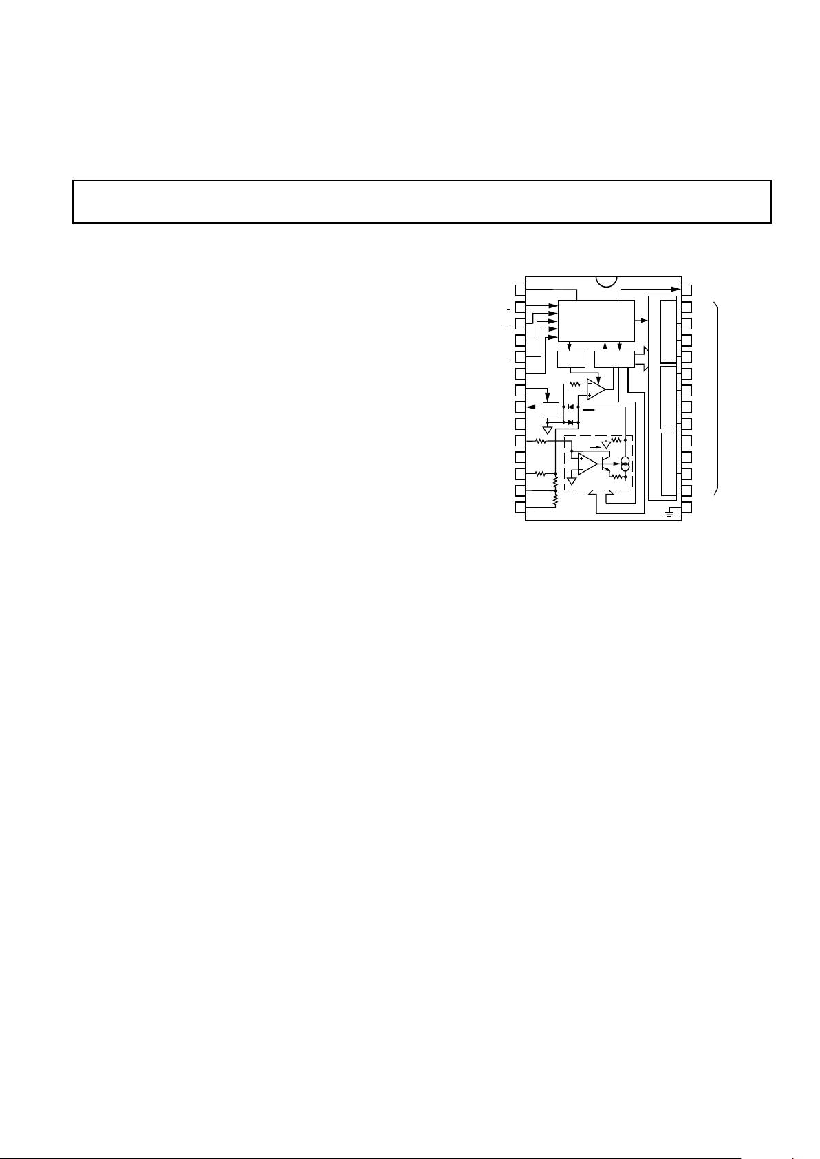
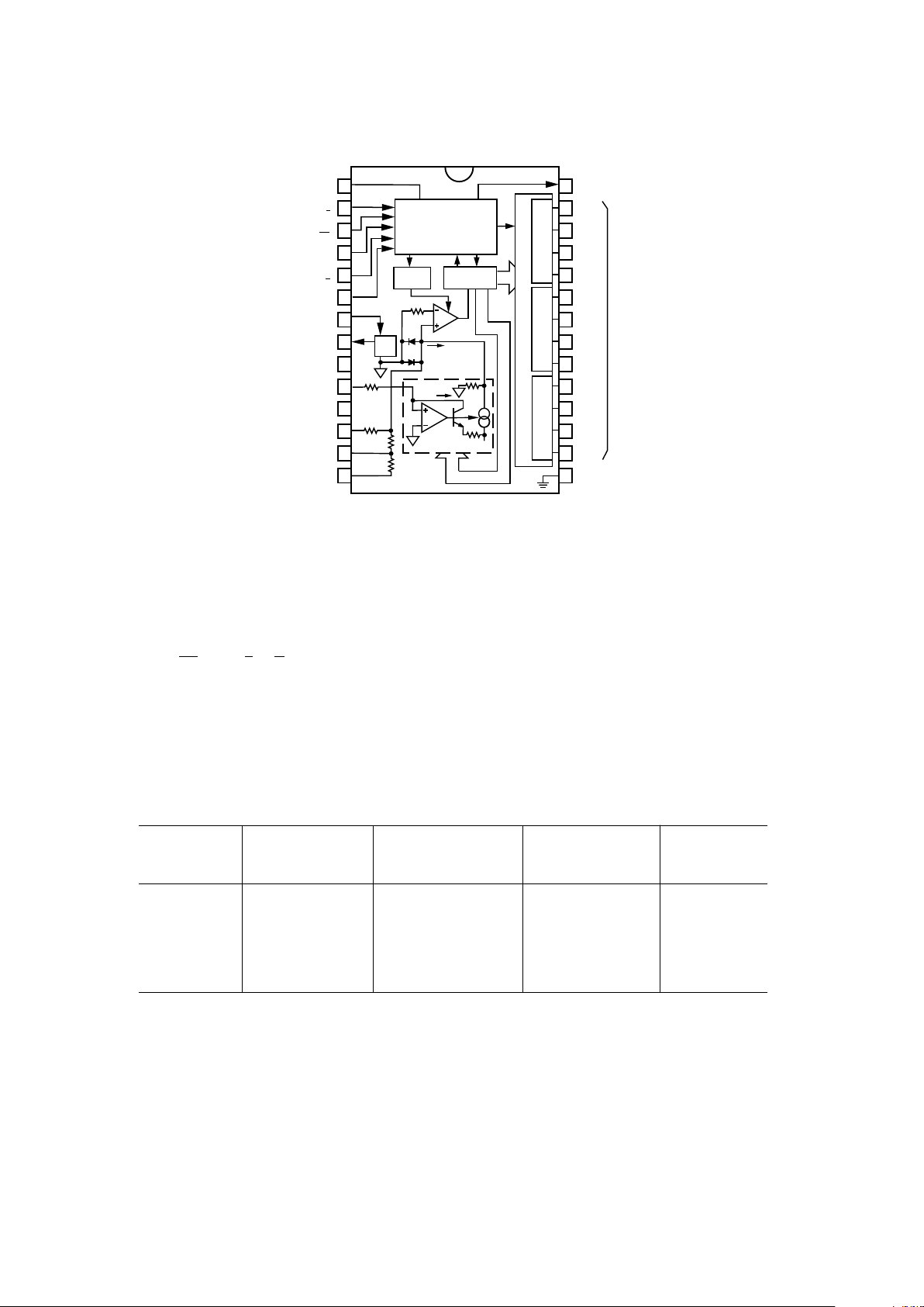
AD574A Block Diagram and Pin Configuration
ABSOLUTE MAXIMUM RATINGS*
(Specifications apply to all grades, except where noted)
VCC to Digital Common . . . . . . . . . . . . . . . . . . 0 V to +16.5 V
V
EE
to Digital Common . . . . . . . . . . . . . . . . . . . 0 V to –16.5 V
V
LOGIC
to Digital Common . . . . . . . . . . . . . . . . . . 0 V to +7 V
Analog Common to Digital Common . . . . . . . . . . . . . . . ±1 V
Control Inputs (CE,
CS, AO 12/8, R/C) to
Digital Common . . . . . . . . . . . . . . –0.5 V to V
LOGIC
+ 0.5 V
Analog Inputs (REF IN, BIP OFF, 10 V
IN
) to
Analog Common . . . . . . . . . . . . . . . . . . . . . . . . . V
EE
to V
CC
20 VIN to Analog Common . . . . . . . . . . . . . . . . . . . . . . ±24 V
REF OUT . . . . . . . . . . . . . . . . . . Indefinite Short to Common
Momentary Short to V
CC
Chip Temperature . . . . . . . . . . . . . . . . . . . . . . . . . . . . . 175°C
Power Dissipation . . . . . . . . . . . . . . . . . . . . . . . . . . . .825 mW
Lead Temperature (Soldering, 10 sec). . . . . . . . . . . . . +300°C
Storage Temperature (Ceramic) . . . . . . . . . .–65°C to +150°C
(Plastic) . . . . . . . . . . . . . . . . . . . . . . . . . . .–25°C to +100°C
*Stresses above those listed under “Absolute Maximum Ratings” may cause
permanent damage to the device. This is a stress rating only and functional
operation of the device at these or any other conditions above those indicated in the
operational sections of this specification is not implied. Exposure to absolute
maximum rating conditions for extended periods may affect device reliability.
Page 5

AD574A
REV. B
–5–
DEFINITIONS OF SPECIFICATIONS
LINEARITY ERROR
Linearity error refers to the deviation of each individual code
from a line drawn from “zero” through “full scale”. The point
used as “zero” occurs 1/2 LSB (1.22 mV for 10 volt span) before the first code transition (all zeros to only the LSB “on”).
“Full scale” is defined as a level 1 1/2 LSB beyond the last code
transition (to all ones). The deviation of a code from the true
straight line is measured from the middle of each particular
code.
The AD574AK, L, T, and U grades are guaranteed for maximum nonlinearity of ±1/2 LSB. For these grades, this means
that an analog value which falls exactly in the center of a given
code width will result in the correct digital output code. Values
nearer the upper or lower transition of the code width may produce the next upper or lower digital output code. The AD574AJ
and S grades are guaranteed to ± 1 LSB max error. For these
grades, an analog value which falls within a given code width
will result in either the correct code for that region or either
adjacent one.
Note that the linearity error is not user-adjustable.
DIFFERENTIAL LINEARITY ERROR (NO MISSING
CODES)
A specification which guarantees no missing codes requires that
every code combination appear in a monotonic increasing sequence as the analog input level is increased. Thus every code
must have a finite width. For the AD574AK, L, T, and U
grades, which guarantee no missing codes to 12-bit resolution,
all 4096 codes must be present over the entire operating temperature ranges. The AD574AJ and S grades guarantee no missing codes to 11-bit resolution over temperature; this means that
all code combinations of the upper 11 bits must be present; in
practice very few of the 12-bit codes are missing.
UNIPOLAR OFFSET
The first transition should occur at a level 1/2 LSB above analog
common. Unipolar offset is defined as the deviation of the actual
transition from that point. This offset can be adjusted as discussed
on the following two pages. The unipolar offset temperature
coefficient specifies the maximum change of the transition point
over temperature, with or without external adjustment.
BIPOLAR OFFSET
In the bipolar mode the major carry transition (0111 1111 1111
to 1000 0000 0000) should occur for an analog value 1/2 LSB
below analog common. The bipolar offset error and temperature
coefficient specify the initial deviation and maximum change in
the error over temperature.
QUANTIZATION UNCERTAINTY
Analog-to-digital converters exhibit an inherent quantization
uncertainty of ±1/2 LSB. This uncertainty is a fundamental
characteristic of the quantization process and cannot be reduced
for a converter of given resolution.
LEFT-JUSTIFIED DATA
The data format used in the AD574A is left-justified. This
means that the data represents the analog input as a fraction of
full-scale, ranging from 0 to
4095
4096
. This implies a binary point
to the left of the MSB
.
FULL-SCALE CALIBRATION ERROR
The last transition (from 1111 1111 1110 to 1111 1111 1111)
should occur for an analog value 1 1/2 LSB below the nominal
full scale (9.9963 volts for 10.000 volts full scale). The full-scale
calibration error is the deviation of the actual level at the last
transition from the ideal level. This error, which is typically
0.05% to 0.1% of full scale, can be trimmed out as shown in
Figures 3 and 4.
TEMPERATURE COEFFICIENTS
The temperature coefficients for full-scale calibration, unipolar
offset, and bipolar offset specify the maximum change from the
initial (25°C) value to the value at T
MIN
or T
MAX
.
POWER SUPPLY REJECTION
The standard specifications for the AD574A assume use of
+5.00 V and ±15.00 V or ±12.00 V supplies. The only effect of
power supply error on the performance of the device will be a
small change in the full-scale calibration. This will result in a
linear change in all lower order codes. The specifications show
the maximum full-scale change from the initial value with the
supplies at the various limits.
CODE WIDTH
A fundamental quantity for A/D converter specifications is the
code width. This is defined as the range of analog input values
for which a given digital output code will occur. The nominal
value of a code width is equivalent to 1 least significant bit
(LSB) of the full-scale range or 2.44 mV out of 10 volts for a
12-bit ADC.
THE AD574A OFFERS GUARANTEED MAXIMUM LINEARITY ERROR OVER THE FULL OPERATING
TEMPERATURE RANGE
Page 6

AD574A
REV. B–6–
CIRCUIT OPERATION
The AD574A is a complete 12-bit A/D converter which requires
no external components to provide the complete successiveapproximation analog-to-digital conversion function. A block
diagram of the AD574A is shown in Figure 1.
1
14
28
15
2
3
4
5
6
7
8
9
10
11
12
13
27
26
25
24
23
22
21
20
19
18
17
16
CONTROL
CLOCK
SAR
3
S
T
A
T
E
O
U
T
P
U
T
B
U
F
F
E
R
S
MSB
N
I
B
B
L
E
N
I
B
B
L
E
N
I
B
B
L
E
LSB
10V
REF
12
12
C
B
A
12
AD574A
3k
19.95k
9.95k
5k
5k
N
DAC
V
EE
8k
I
REF
COMP
DIGITAL COMMON
DC
I
DAC
I
DAC
=
4 x N x I
REF
+5V SUPPLY
V
LOGIC
DATA MODE SELECT
12/8
STATUS
STS
DB11
MSB
DB10
DB9
DB8
DB7
DB6
DB5
DB4
DB3
DB2
DB1
DB0
LSB
DIGITAL
DATA
OUTPUTS
CHIP SELECT
CS
BYTE ADDRESS/
SHORT CYCLE
A
O
READ/CONVERT
R/C
CHIP ENABLE
CE
+12/+15V SUPPLY
V
CC
+10V REFERENCE
REF OUT
ANALOG COMMON
AC
REFERENCE INPUT
REF IN
-12/-15V SUPPLY
V
EE
BIPOLAR OFFSET
BIP OFF
10V SPAN INPUT
10V
IN
20V SPAN INPUT
20V
IN
Figure 1. Block Diagram of AD574A 12-Bit A-to-D Converter
When the control section is commanded to initiate a conversion
(as described later), it enables the clock and resets the successiveapproximation register (SAR) to all zeros. Once a conversion
cycle has begun, it cannot be stopped or restarted and data is
not available from the output buffers. The SAR, timed by the
clock, will sequence through the conversion cycle and return an
end-of-convert flag to the control section. The control section
will then disable the clock, bring the output status flag low, and
enable control functions to allow data read functions by external
command.
During the conversion cycle, the internal 12-bit current output
DAC is sequenced by the SAR from the most significant bit
(MSB) to least significant bit (LSB) to provide an output current which accurately balances the input signal current through
the 5 kΩ (or 10 kΩ) input resistor. The comparator determines
whether the addition of each successively-weighted bit current
causes the DAC current sum to be greater or less than the input
current; if the sum is less, the bit is left on; if more, the bit is
turned off. After testing all the bits, the SAR contains a 12-bit
binary code which accurately represents the input signal to
within ±1/2 LSB.
The temperature-compensated buried Zener reference provides
the primary voltage reference to the DAC and guarantees excellent stability with both time and temperature. The reference is
trimmed to 10.00 volts ±0.2%; it can supply up to 1.5 mA to an
external load in addition to the requirements of the reference input resistor (0.5 mA) and bipolar offset resistor (1 mA) when
the AD574A is powered from ±15 V supplies. If the AD574A is
used with ±12 V supplies, or if external current must be supplied over the full temperature range, an external buffer amplifier is recommended. Any external load on the AD574A
reference must remain constant during conversion. The
thin-film application resistors are trimmed to match the
full-scale output current of the DAC. There are two 5 kΩ input
scaling resistors to allow either a 10 volt or 20 volt span. The
10 kΩ bipolar offset resistor is grounded for unipolar operation
and connected to the 10 volt reference for bipolar operation.
DRIVING THE AD574 ANALOG INPUT
The internal circuitry of the AD574 dictates that its analog
input be driven by a low source impedance. Voltage changes at
the current summing node of the internal comparator result in
abrupt modulations of the current at the analog input. For accurate 12-bit conversions the driving source must be capable of
holding a constant output voltage under these dynamically
changing load conditions.
CURRENT
OUTPUT
DAC
SAR
COMPARATOR
AD574A
I
IN
i
TEST
R
IN
i
DIFF
V+
V–
FEEDBACK TO AMPLIFIER
ANALOG COMMON
IIN IS MODULATED BY
CHANGES IN TEST CURRENT.
AMPLIFIER PULSE LOAD
RESPONSE LIMITED BY
OPEN LOOP OUTPUT IMPEDANCE.
CURRENT
LIMITING
RESISTORS
Figure 2. Op Amp – AD574A Interface
The output impedance of an op amp has an open-loop value
which, in a closed loop, is divided by the loop gain available at
the frequency of interest. The amplifier should have acceptable
loop gain at 500 kHz for use with the AD574A. To check
whether the output properties of a signal source are suitable,
monitor the AD574’s input with an oscilloscope while a conversion is in progress. Each of the 12 disturbances should subside
in 1 µs or less.
For applications involving the use of a sample-and-hold amplifier, the AD585 is recommended. The AD711 or AD544 op
amps are recommended for dc applications.
SAMPLE-AND-HOLD AMPLIFIERS
Although the conversion time of the AD574A is a maximum of
35 µs, to achieve accurate 12-bit conversions of frequencies
greater than a few Hz requires the use of a sample-and-hold
amplifier (SHA). If the voltage of the analog input signal driving
the AD574A changes by more than 1/2 LSB over the time
interval needed to make a conversion, then the input requires a
SHA.
The AD585 is a high linearity SHA capable of directly driving
the analog input of the AD574A. The AD585’s fast acquisition
time, low aperture and low aperture jitter are ideally suited for
high-speed data acquisition systems. Consider the AD574A
converter with a 35 µs conversion time and an input signal of
10 V p-p: the maximum frequency which may be applied to
achieve rated accuracy is 1.5 Hz. However, with the addition of
an AD585, as shown in Figure 3, the maximum frequency
increases to 26 kHz.
The AD585’s low output impedance, fast-loop response, and
low droop maintain 12-bits of accuracy under the changing load
conditions that occur during a conversion, making it suitable for
use in high accuracy conversion systems. Many other SHAs
cannot achieve 12-bits of accuracy and can thus compromise a
system. The AD585 is recommended for AD574A applications
requiring a sample and hold.
An alternate approach is to use the AD1674, which combines
the ADC and SHA on one chip, with a total throughput time of
10 µs.
Page 7

AD574A
REV. B
–7–
A
8
10
13
12
3
15
4
9
A2
AD574A
27
16
12-BIT
3-STATE
DATA
+
C3
C1
C2
+
+
+15V
+5V
–15V
+V
S
TO A1
–V
S
TO A1
14 13 12 11 10 9 8
1234567
A
R4
100k
+15V
–15V
R1
100k
OFFSET
R3
100Ω
7404 OR EQ.
CONVERT
STATUS
GAIN
R2
100Ω
V
REF
AGND
+V
S
–V
S
ANALOG
INPUT
0V TO +10V
10k 10k
100pF
A1
AD585
176211
NOTE
1. C1, C2, C3 ARE 47mF TANTALUM, BYPASSED BY
0.1mF CERAMIC. LOCATE AT ASSOCIATED A2 PINS.µ
µ
28
5
Figure 3. AD574A with AD585 Sample and Hold
SUPPLY DECOUPLING AND LAYOUT
CONSIDERATIONS
It is critically important that the AD574A power supplies be filtered, well regulated, and free from high frequency noise. Use of
noisy supplies will cause unstable output codes. Switching
power supplies are not recommended for circuits attempting to
achieve 12-bit accuracy unless great care is used in filtering any
switching spikes present in the output. Remember that a few
millivolts of noise represents several counts of error in a 12-bit
ADC.
Decoupling capacitors should be used on all power supply pins;
the +5 V supply decoupling capacitor should be connected
directly from Pin 1 to Pin 15 (digital common) and the +V
CC
and –VEE pins should be decoupled directly to analog common
(Pin 9). A suitable decoupling capacitor is a 4.7 µF tantalum
type in parallel with a 0.1 µF disc ceramic type.
Circuit layout should attempt to locate the AD574A, associated
analog input circuitry, and interconnections as far as possible
from logic circuitry. For this reason, the use of wire-wrap circuit
construction is not recommended. Careful printed circuit construction is preferred.
GROUNDING CONSIDERATIONS
The analog common at Pin 9 is the ground reference point for
the internal reference and is thus the “high quality” ground for
the AD574A; it should be connected directly to the analog reference point of the system. In order to achieve all of the high
accuracy performance available from the AD574A in an environment of high digital noise content, the analog and digital
commons should be connected together at the package. In some
situations, the digital common at Pin 15 can be connected to
the most convenient ground reference point; analog power
return is preferred.
UNIPOLAR RANGE CONNECTIONS FOR THE AD574A
The AD574A contains all the active components required to
perform a complete 12-bit A/D conversion. Thus, for most situations, all that is necessary is connection of the power supplies
(+5 V, +12 V/+15 V and –12 V/–15 V), the analog input, and
the conversion initiation command, as discussed on the next
page. Analog input connections and calibration are easily accomplished; the unipolar operating mode is shown in Figure 4.
9
14
13
12
8
10
6
5
4
3
2
28
15
11
7
1
27
24
19
16
23
20
AD574A
STS
HIGH
BIT
MIDDLE
BITS
LOW
BITS
+5V
+15V
–15V
DIG COM
12/8
CS
A
O
R/C
CE
REF IN
REF OUT
BIP OFF
10V
IN
20V
IN
ANA COM
OFFSET
R1
100k
–12V/–15V
+12V/+15V
GAIN
100k
R2
100Ω
100Ω
ANALOG
INPUTS
0 TO +10V
0 TO +20V
Figure 4. Unipolar Input Connections
All of the thin-film application resistors of the AD574A are
trimmed for absolute calibration. Therefore, in many applications, no calibration trimming will be required. The absolute
accuracy for each grade is given in the specification tables.
For example, if no trims are used, the AD574AK guarantees
±1 LSB max zero offset error and ±0.25% (10 LSB) max
full-scale error. (Typical full-scale error is ± 2 LSB.) If the offset
trim is not required, Pin 12 can be connected directly to Pin 9;
the two resistors and trimmer for Pin 12 are then not needed. If
the full-scale trim is not needed, a 50 Ω ± 1% metal film resistor
should be connected between Pin 8 and Pin 10.
The analog input is connected between Pin 13 and Pin 9 for a
0 V to +10 V input range, between 14 and Pin 9 for a 0 V to
+20 V input range. The AD574A easily accommodates an input
signal beyond the supplies. For the 10 volt span input, the LSB
has a nominal value of 2.44 mV; for the 20 volt span, 4.88 mV.
If a 10.24 V range is desired (nominal 2.5 mV/bit), the gain
trimmer (R2) should be replaced by a 50 Ω resistor, and a
200 Ω trimmer inserted in series with the analog input to Pin 13
for a full-scale range of 20.48 V (5 mV/bit), use a 500 Ω trimmer into Pin 14. The gain trim described below is now done
with these trimmers. The nominal input impedance into Pin 13
is 5 kΩ, and 10 kΩ into Pin 14.
UNIPOLAR CALIBRATION
The AD574A is intended to have a nominal 1/2 LSB offset so
that the exact analog input for a given code will be in the middle
of that code (halfway between the transitions to the codes above
and below it). Thus, the first transition (from 0000 0000 0000
to 0000 0000 0001) will occur for an input level of +1/2 LSB
(1.22 mV for 10 V range).
If Pin 12 is connected to Pin 9, the unit will behave in this manner, within specifications. If the offset trim (R1) is used, it
should be trimmed as above, although a different offset can be
set for a particular system requirement. This circuit will give approximately ±15 mV of offset trim range.
Page 8

AD574A
REV. B–8–
The full-scale trim is done by applying a signal 1 1/2 LSB below
the nominal full scale (9.9963 for a 10 V range). Trim R2 to
give the last transition (1111 1111 1110 to 1111 1111 1111).
BIPOLAR OPERATION
The connections for bipolar ranges are shown in Figure 5.
Again, as for the unipolar ranges, if the offset and gain specifications are sufficient, one or both of the trimmers shown can be
replaced by a 50 Ω ± 1% fixed resistor. Bipolar calibration is
similar to unipolar calibration. First, a signal 1/2 LSB above
negative full scale (–4.9988 V for the ± 5 V range) is applied and
R1 is trimmed to give the first transition (0000 0000 0000 to
0000 0000 0001). Then a signal 1 1/2 LSB below positive full
scale (+4.9963 V the ±5 V range) is applied and R2 trimmed to
give the last transition (1111 11111110 to 1111 1111 1111).
9
14
13
12
8
10
6
5
4
3
2
28
15
11
7
1
27
24
19
16
23
20
AD574A
STS
HIGH
BIT
MIDDLE
BITS
LOW
BITS
+5V
+15V
–15V
DIG COM
12/8
CS
A
O
R/C
CE
REF IN
REF OUT
BIP OFF
10V
IN
20V
IN
ANA COM
GAIN
R2
100Ω
ANALOG
INPUTS
65V
R1
100Ω
610V
OFFSET
Figure 5. Bipolar Input Connections
CONTROL LOGIC
The AD574A contains on-chip logic to provide conversion initiation and data read operations from signals commonly available in microprocessor systems. Figure 6 shows the internal
logic circuitry of the AD574A.
The control signals CE,
CS, and R/C control the operation of
the converter. The state of R/
C when CE and CS are both
asserted determines whether a data read (R/
C = 1) or a convert
(R/
C = 0) is in progress. The register control inputs AO and
12/
8 control conversion length and data format. The AO line is
usually tied to the least significant bit of the address bus. If a
conversion is started with A
O
low, a full 12-bit conversion cycle
is initiated. If A
O
is high during a convert start, a shorter 8-bit
conversion cycle results. During data read operations, A
O
determines whether the three-state buffers containing the 8 MSBs of
the conversion result (A
O
= 0) or the 4 LSBs (AO = 1) are
enabled. The 12/
8 pin determines whether the output data is
to be organized as two 8-bit words (12/
8 tied to DIGITAL
COMMON) or a single 12-bit word (12/
8 tied to V
LOGIC
). The
12/
8 pin is not TTL-compatible and must be hard-wired to
either V
LOGIC
or DIGITAL COMMON. In the 8-bit mode, the
byte addressed when A
O
is high contains the 4 LSBs from the
conversion followed by four trailing zeroes. This organization
allows the data lines to be overlapped for direct interface to
8-bit buses without the need for external three-state buffers.
It is not recommended that A
O
change state during a data read
operation. Asymmetrical enable and disable times of the
three-state buffers could cause internal bus contention resulting
in potential damage to the AD574A.
READ
CONVERT
LOW IF CONVERSION
IN PROGRESS
VALUE OF A0
AT LAST CONVERT
COMMAND
EOC8
EOC12
FROM
NOTE 1
NIBBLE A, B,
ENABLE
NIBBLE C
ENABLE
NIBBLE B = O
ENABLE
TO OUTPUT
BUFFERS
START CONVERT
STATUS
R/C
CE
CS
A0
12/8
(NOTE 2)
NOTE 1: WHEN START CONVERT GOES LOW, THE EOC (END OF CONVERSION) SIGNALS GO LOW.
EOC8 RETURNS HIGH AFTER AN 8-BIT CONVERSION CYCLE IS COMPLETE, AND EOC12
RETURNS HIGH WHEN ALL 12-BITS HAVE BEEN CONVERTED. THE EOC SIGNALS PREVENT
DATA FROM BEING READ DURING CONVERSIONS.
NOTE 2: 12/8 IS NOT A TTL-COMPATABLE INPUT AND SHOULD ALWAYS BE WIRED DIRECTLY TO
V
LOGIC
OR DIGITAL COMMON.
Figure 6. AD574A Control Logic
An output signal, STS, indicates the status of the converter.
STS goes high at the beginning of a conversion and returns low
when the conversion cycle is complete.
Table I. AD574A Truth Table
CE CS R/C 12/8 AOOperation
0 X X X X None
X 1 X X X None
1 0 0 X 0 Initiate 12-Bit Conversion
1 0 0 X 1 Initiate 8-Bit Conversion
1 0 1 Pin 1 X Enable 12-Bit Parallel Output
1 0 1 Pin 15 0 Enable 8 Most Significant Bits
1 0 1 Pin 15 1 Enable 4 LSBs + 4 Trailing Zeroes
TIMING
The AD574A is easily interfaced to a wide variety of microprocessors and other digital systems. The following discussion of
the timing requirements of the AD574A control signals should
provide the system designer with useful insight into the operation of the device.
Table II. Convert Start Timing—Full Control Mode
Symbol Parameter Min Typ Max Units
t
DSC
STS Delay from CE 400 ns
t
HEC
CE Pulse Width 300 ns
t
SSC
CS to CE Setup 300 ns
t
HSC
CS Low During CE High 200 ns
t
SRC
R/C to CE Setup 250 ns
t
HRC
R/C Low During CE High 200 ns
t
SAC
AO to CE Setup 0 ns
t
HAC
AO Valid During CE High 300 ns
t
C
Conversion Time
8-Bit Cycle 10 24 µs
12-Bit Cycle 15 35 µs
Page 9

AD574A
REV. B
–9–
Figure 7 shows a complete timing diagram for the AD574A convert start operation. R/
C should be low before both CE and CS
are asserted; if R/
C is high, a read operation will momentarily
occur, possibly resulting in system bus contention. Either CE or
CS may be used to initiate a conversion; however, use of CE is
recommended since it includes one less propagation delay than
CS and is the faster input. In Figure 7, CE is used to initiate the
conversion.
Figure 7. Convert Start Timing
Once a conversion is started and the STS line goes high, convert
start commands will be ignored until the conversion cycle is
complete. The output data buffers cannot be enabled during
conversion.
Figure 8 shows the timing for data read operations. During data
read operations, access time is measured from the point where
CE and R/
C both are high (assuming CS is already low). If CS
is used to enable the device, access time is extended by 100 ns.
Figure 8. Read Cycle Timing
In the 8-bit bus interface mode (12/8 input wired to DIGITAL
COMMON), the address bit, A
O
, must be stable at least 150 ns
prior to
CE going high and must remain stable during the entire
read cycle. If A
O
is allowed to change, damage to the AD574A
output buffers may result.
Table III. Read Timing—Full Control Mode
Symbol Parameter Min Typ Max Units
t
DD
1
Access Time (from CE) 200 ns
t
HD
Data Valid After CE Low 25 ns
t
HL
2
Output Float Delay 100 ns
t
SSR
CS to CE Setup 150 ns
t
SRR
R/C to CE Setup 0 ns
t
SAR
AO to CE Setup 150 ns
t
HSR
CS Valid After CE Low 50 ns
t
HRR
R/C High After CE Low 0 ns
t
HAR
AO Valid After CE Low 50 ns
NOTES
1
tDD is measured with the load circuit of Figure 9 and defined as the time
required for an output to cross 0.4 V or 2.4 V.
2
tHL is defined as the time required for the data lines to change 0.5 V when
loaded with the circuit of Figure 10.
a. High-Z to Logic 1 b. High-Z to Logic 0
Figure 9. Load Circuit for Access Time Test
a. Logic 1 to High-Z b. Logic 0 to High-Z
Figure 10. Load Circuit for Output Float Delay Test
“STAND-ALONE” OPERATION
The AD574A can be used in a “stand-alone” mode, which is
useful in systems with dedicated input ports available and thus
not requiring full bus interface capability.
In this mode, CE and 12/
8 are wired high, CS and AO are wired
low, and conversion is controlled by R/
C. The three-state buff-
ers are enabled when R/
C is high and a conversion starts when
R/
C goes low. This allows two possible control signals—a high
pulse or a low pulse. Operation with a low pulse is shown in
Figure 11. In this case, the outputs are forced into the high
impedance state in response to the falling edge of R/
C and return
Figure 11. Low Pulse for R/C—Outputs Enabled After
Conversion
Page 10

AD574A
REV. B–10–
to valid logic levels after the conversion cycle is completed. The
STS line goes high 600 ns after R/
C goes low and returns low
300 ns after data is valid.
If conversion is initiated by a high pulse as shown in Figure 12,
the data lines are enabled during the time when R/
C is high.
The falling edge of R/
C starts the next conversion, and the data
lines return to three-state (and remain three-state) until the next
high pulse of R/
C.
Figure 12. High Pulse for R/C—Outputs Enabled While R/
C
High, Otherwise High-Z
Table IV. Stand-Alone Mode Timing
Symbol Parameter Min Typ Max Units
t
HRL
Low R/C Pulse Width 250 ns
t
DS
STS Delay from R/C 600 ns
t
HDR
Data Valid After R/C Low 25 ns
t
HL
Output Float Delay 150 ns
t
HS
STS Delay After Data Valid 300 1000 ns
t
HRH
High R/C Pulse Width 300 ns
t
DDR
Data Access Time 250 ns
Usually the low pulse for R/C stand-alone mode will be used.
Figure 13 illustrates a typical stand-alone configuration for 8086
type processors. The addition of the 74F/S374 latches improves
bus access/release times and helps minimize digital feedthrough
to the analog portion of the converter.
Figure 13. 8086 Stand-Alone Configuration
INTERFACING THE AD574A TO MICROPROCESSORS
The control logic of the AD574A makes direct connection to
most microprocessor system buses possible. While it is impossible to describe the details of the interface connections for every
microprocessor type, several representative examples will be
described here.
GENERAL A/D CONVERTER INTERFACE
CONSIDERATIONS
A typical A/D converter interface routine involves several
operations. First, a write to the ADC address initiates a conversion. The processor must then wait for the conversion cycle to
complete, since most ADCs take longer than one instruction
cycle to complete a conversion. Valid data can, of course, only
be read after the conversion is complete. The AD574A provides
an output signal (STS) which indicates when a conversion is in
progress. This signal can be polled by the processor by reading
it through an external three-state buffer (or other input port).
The STS signal can also be used to generate an interrupt upon
completion of conversion, if the system timing requirements are
critical (bear in mind that the maximum conversion time of the
AD574A is only 35 microseconds) and the processor has other
tasks to perform during the ADC conversion cycle. Another
possible time-out method is to assume that the ADC will take
35 microseconds to convert, and insert a sufficient number of
“do-nothing” instructions to ensure that 35 microseconds of
processor time is consumed.
Once it is established that the conversion is finished, the data
can be read. In the case of an ADC of 8-bit resolution (or less),
a single data read operation is sufficient. In the case of converters with more data bits than are available on the bus, a choice of
data formats is required, and multiple read operations are needed.
The AD574A includes internal logic to permit direct interface
to 8-bit or 16-bit data buses, selected by connection of the 12/
8
input. In 16-bit bus applications (12/
8 high) the data lines
(DB11 through DB0) may be connected to either the 12 most
significant or 12 least significant bits of the data bus. The remaining four bits should be masked in software. The interface
to an 8-bit data bus (12/
8 low) is done in a left-justified format.
The even address (A0 low) contains the 8 MSBs (DB11 through
DB4). The odd address (A0 high) contains the 4 LSBs (DB3
through DB0) in the upper half of the byte, followed by four
trailing zeroes, thus eliminating bit masking instructions.
It is not possible to rearrange the AD574A data lines for right
justified 8-bit bus interface.
Figure 14. AD574A Data Format for 8-Bit Bus
SPECIFIC PROCESSOR INTERFACE EXAMPLES
Z-80 System Interface
The AD574A may be interfaced to the Z-80 processor in an I/O
or memory mapped configuration. Figure 15 illustrates an I/O
or mapped configuration. The Z-80 uses address lines A0–A7 to
decode the I/O port address.
An interesting feature of the Z-80 is that during I/O operations a
single wait state is automatically inserted, allowing the AD574A
to be used with Z-80 processors having clock speeds up to 4 MHz.
For applications faster than 4 MHz use the wait state generator
in Figure 16. In a memory mapped configuration the AD574A
may be interfaced to Z-80 processors with clock speeds of up to
2.5 MHz.
Page 11

AD574A
REV. B
–11–
Figure 15. Z80—AD574A Interface
Figure 16. Wait State Generator
IBM PC Interface
The AD574A appears in Figure 17 interfaced to the 4 MHz
8088 processor of an IBM PC. Since the device resides in I/O
space, its address is decoded from only the lower ten address
lines and must be gated with AEN (active low) to mask out internal DMA cycles which use the same I/O address space. This
active low signal is applied to
CS. IOR and IOW are used to
initiate the conversion and read, and are gated together to drive
the chip enable, CE. Because the data bus width is limited to
8 bits, the AD574A data resides in two adjacent addresses
selected by A0.
Figure 17. IBM PC—AD574A Interface
Note: Due to the large number of options that may be installed
in the PC, the I/O bus loading should be limited to one Schottky
TTL load. Therefore, a buffer/driver should be used when interfacing more than two AD574As to the I/O bus.
8086 Interface
The data mode select pin (12/8) of the AD574A should be connected to V
LOGIC
to provide a 12-bit data output. To prevent
possible bus contention, a demultiplexed and buffered address/
data bus is recommended. In the cases where the 8-bit short
conversion cycle is not used, A0 should be tied to digital common. Figure 18 shows a typical 8086 configuration.
Figure 18. 8086—AD574A with Buffered Bus lnterface
For clock speeds greater than 4 MHz wait state insertion similar
to Figure 16 is recommended to ensure sufficient CE and R/
C
pulse duration.
The AD574A can also be interfaced in a stand-alone mode (see
Figure 13). A low going pulse derived from the 8086’s
WR signal logically ORed with a low address decode starts the conversion. At the end of the conversion, STS clocks the data into the
three-state latches.
68000 Interface
The AD574, when configured in the stand-alone mode, will easily interface to the 4 MHz version of the 68000 microprocessor.
The 68000 R/
W signal combined with a low address decode ini-
tiates conversion. The
UDS or LDS signal, with the decoded
address, generates the
DTACK input to the processor, latching
in the AD574A’s data. Figure 19 illustrates this configuration.
Figure 19. 68000—AD574A Interface
Page 12

AD574A
REV. B–12–
OUTLINE DIMENSIONS
Dimensions shown in inches and (mm).
28-Pin Ceramic DIP Package (D-28) 28-Lead Plastic DIP Package (N-28A)
28-Terminal PLCC Package (P-28A)
4
PIN 1
IDENTIFIER
5
26
25
11
12
19
18
TOP VIEW
(PINS DOWN)
0.495 (12.57)
0.485 (12.32)
SQ
0.456 (11.58)
0.450 (11.43)
SQ
0.048 (1.21)
0.042 (1.07)
0.048 (1.21)
0.042 (1.07)
0.020
(0.50)
R
0.050
(1.27)
BSC
0.021 (0.53)
0.013 (0.33)
0.430 (10.92)
0.390 (9.91)
0.032 (0.81)
0.026 (0.66)
0.180 (4.57)
0.165 (4.19)
0.040 (1.01)
0.025 (0.64)
0.056 (1.42)
0.042 (1.07)
0.025 (0.63)
0.015 (0.38)
0.110 (2.79)
0.085 (2.16)
28–Terminal LCC Package (E-28A)
0.075
(1.91)
REF
0.075 (1.91) REF
SQ
0.458 (11.63)
0.442 (11.23)
TOP VIEW
0.088 (2.24)
0.054 (1.37)
0.100 (2.54)
0.064 (1.63)
0.458
(11.63)
MAX
SQ
0.150 (3.81) BSC
0.011 (0.28)
0.007 (0.18)
R TYP
BOTTOM
VIEW
1
28
18
12
0.095 (2.41)
0.075 (1.90)
0.055 (1.40)
0.045 (1.14)
45
°
TYP
0.200
(5.08)
BSC
0.015 (0.38)
MIN
0.028 (0.71)
0.022 (0.56)
0.050
(1.27)
BSC
0.300 (7.62) BSC
C704d–10–8/88
PRINTED IN U.S.A.
 Loading...