

Page 1
16-Bit Monotonic
a
FEATURES
Guaranteed 16-Bit Monotonicity
Monolithic BiMOS II Construction
60.01% Typical Nonlinearity
8- and 16-Bit Bus Compatibility
3 ms Settling to 16 Bits
Low Drift
Low Power
Low Noise
APPLICATIONS
Robotics
Closed-Loop Positioning
High-Resolution ADCs
Microprocessor-Based Process Control
MIL-STD-883 Compliant Versions Available
PRODUCT DESCRIPTION
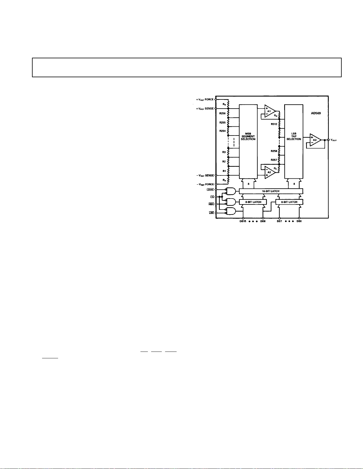
The AD569 is a monolithic 16-bit digital-to-analog converter
(DAC) manufactured in Analog Devices’ BiMOS II process.
BiMOS II allows the fabrication of low power CMOS logic
functions on the same chip as high precision bipolar linear circuitry. The AD569 chip includes two resistor strings, selector
switches decoding logic, buffer amplifiers, and double-buffered
input latches.
The AD569’s voltage-segmented architecture insures 16-bit
monotonicity over time and temperature. Integral nonlinearity is
maintained at ±0.01%, while differential nonlinearity is
±0.0004%. The on-chip, high-speed buffer amplifiers provide a
voltage output settling time of 3 µs to within ±0.001% for a
full-scale step.
The reference input voltage which determines the output range
can be either unipolar or bipolar. Nominal reference range is
±5 V and separate reference force and sense connections are
provided for high accuracy applications. The AD569 can operate with an ac reference in multiplying applications.
Data may be loaded into the AD569’s input latches from 8- and
16-bit buses. The double-buffered structure simplifies 8-bit bus
interfacing and allows multiple DACs to be loaded asynchronously and updated simultaneously. Four TTL/LSTTL/5 V
CMOS-compatible signals control the latches:
and
LDAC
The AD569 is available in five grades: J and K versions are
specified from 0°C to +70°C and are packaged in a 28-pin plastic DIP and 28-pin PLCC package; AD and BD versions are
specified from –25°C to +85°C and are packaged in a 28-pin
ceramic DIP. The SD version, also in a 28-pin ceramic DIP, is
specified from –55°C to +125°C.
CS, LBE, HBE,
Voltage Output D/A Converter
AD569
FUNCTIONAL BLOCK DIAGRAM
PRODUCT HIGHLIGHTS
1. Monotonicity to 16 bits is insured by the AD569’s voltagesegmented architecture.
2. The output range is ratiometric to an external reference or ac
signal. Gain error and gain drift of the AD569 are negligible.
3. The AD569’s versatile data input structure allows loading
from 8- and 16-bit buses.
4. The on-chip output buffer amplifier can supply ± 5 V into a
1 kΩ load, and can drive capacitive loads of up to 1000 pF.
5. Kelvin connections to the reference inputs preserve the gain
and offset accuracy of the transfer function in the presence of
wiring resistances and ground currents.
6. The AD569 is available in versions compliant with MIL-STD-
883. Refer to the Analog Devices Military Products Databook or current AD569/883B data sheet for detailed
specifications.
REV. A
Information furnished by Analog Devices is believed to be accurate and
reliable. However, no responsibility is assumed by Analog Devices for its
use, nor for any infringements of patents or other rights of third parties
which may result from its use. No license is granted by implication or
otherwise under any patent or patent rights of Analog Devices.
One Technology Way, P.O. Box 9106, Norwood, MA 02062-9106, U.S.A.
Tel: 617/329-4700 Fax: 617/326-8703
Page 2

AD569–SPECIFICATIONS
(TA = +258C, +VS = +12 V, –VS = –12 V, +V
otherwise noted.)
= +5 V, –V
REF
= –5 V, unless
REF
Model AD569JN/JP/AD AD569KN/KP/BD AD569SD
Parameter Min Typ Max Min Typ Max Min Typ Max Units
RESOLUTION 16 16 16 Bits
LOGIC INPUTS
V
(Logic “l”) 2.0 5.5 2.0 5.5 2.0 5.5 Volts
IH
V
(Logic “0”) 0 0.8 0 0.8 0 0.8 Volts
IL
I
(VIH = 5.5 V) 10 10 10 µA
IH
IIL (VIL = 0 V) 10 10 10 µA
TRANSFER FUNCTION
CHARACTERISTICS
Integral Nonlinearity ±0.02
T
MIN
to T
MAX
±0.02
Differential Nonlinearity ±1/2
T
to T
MIN
MAX
MAX
MAX
MAX
2
MAX
3
2
2
2
–5 +5 –5 +5 –5 +5 Volts
Unipolar Offset
T
to T
MIN
Bipolar Offset
T
to T
MIN
Full Scale Error
T
to T
MIN
Bipolar Zero
T
to T
MIN
REFERENCE INPUT
+V
Range
REF
–V
Range –5 +5 –5 +5 –5 +5 Volts
REF
±1/2
Resistance 15 20 25 15 20 25 15 20 25 kΩ
6
0.04 ±0.01
6
0.04 ±0.02060.024
6
1 ±1/4
6
1 ±1/2
6
500
6
750
6
500
6
750
6
350
6
750
6
0.04
6
0.04
6
0.024
6
1/2
6
1
6
350
6
450
6
350
6
450
6
350
6
750
6
0.024
6
0.024
6
0.04 % FSR
6
0.04 % FSR
6
1 LSB
6
1 LSB
6
500 µV
6
750 µV
6
500 µV
6
750 µV
6
350 µV
6
750 µV
6
0.04 % FSR
6
0.04 % FSR
4
1
OUTPUT CHARACTERISTICS
Voltage –5 +5 –5 +5 –5 +5 Volts
Capacitive Load 1000 1000 1000 pF
Resistive Load 1 1 1 kΩ
Short Circuit Current 10 10 10 mA
POWER SUPPLIES
Voltage
+V
–V
S
S
+10.8 +12 +13.2 +10.8 +12 +13.2 +10.8 +12 +13.2 Volts
–10.8 –12 –13.2 –10.8 –12 –13.2 –10.8 –12 –13.2 Volts
Current
+I
S
–I
S
Power Supply Sensitivity
5
+9 +13 +9 +13 +9 +13 mA
–9 –13 –9 –13 –9 –13 mA
+10.8 V ≤ +VS ≤ +13.2 V ±0.5 62 ±0.5 62 ±0.5 62 ppm/%
–10.8 V ≥ –VS ≥ –13.2 V ±1 63 ±1 63 ±1 63 ppm/%
TEMPERATURE RANGE
Specified
JN, KN, JP, KP 0 +70 0 +70 °C
AD, BD –25 +85 –25 +85 °C
SD –55 +125 °C
Storage
JN, KN, JP, KP –65 +150 –65 +150 °C
AD, BD, SD –65 +150 –65 +150 –65 +150 °C
NOTES
1
FSR stands for Full-Scale Range, and is 10 V for a –5 V to +5 V span.
2
Refer to Definitions section.
3
For operation with supplies other than ±12 V, refer to the Power Supply and Reference Voltage Range Section.
4
Measured between +V
5
Sensitivity of Full-Scale Error due to changes in +VS and sensitivity of Offset to changes in –VS.
Specifications subject to change without notice.
Specifications shown in boldface are tested on all production units at final electrical test. Results from those tests are used to calculate outgoing quality levels. All min
and max specifications are guaranteed, although only those shown in boldface are tested on all production units.
Force and –V
REF
REF
Force.
–2–
REV. A
Page 3
AC PERFORMANCE CHARACTERISTICS
These characteristics are included for Design Guidance Only and are not subject to test.
+VS = +12 V; –VS = –12 V; +V
Parameter Limit Units Test Conditions/Comments
Output Voltage Settling 5 µs max No Load Applied
(Time to ±0.001% FS 3 µs typ (DAC output measured from falling edge of
For FS Step) 6 µs max V
= +5 V; –V
REF
= –5 V excepts where stated.
REF
Load = 1 kΩ, C
OUT
= 1000 pF.
LOAD
4 µs typ (DAC output measured from falling edge of LDAC. )
AD569
LDAC.)
Digital-to-Analog Glitch 500 nV-sec typ Measured with V
= 0 V. DAC registers alternatively loaded
REF
Impulse with input codes of 8000
transition). Load = 1 kΩ.
Multiplying Feedthrough –100 dB max +V
= 1 V rms 10 kHz sine wave,
REF
–V
= 0 V
REF
Output Noise Voltage 40 nV/ÏHz typ Measured between V
Density (1 kHz-1 MHz)
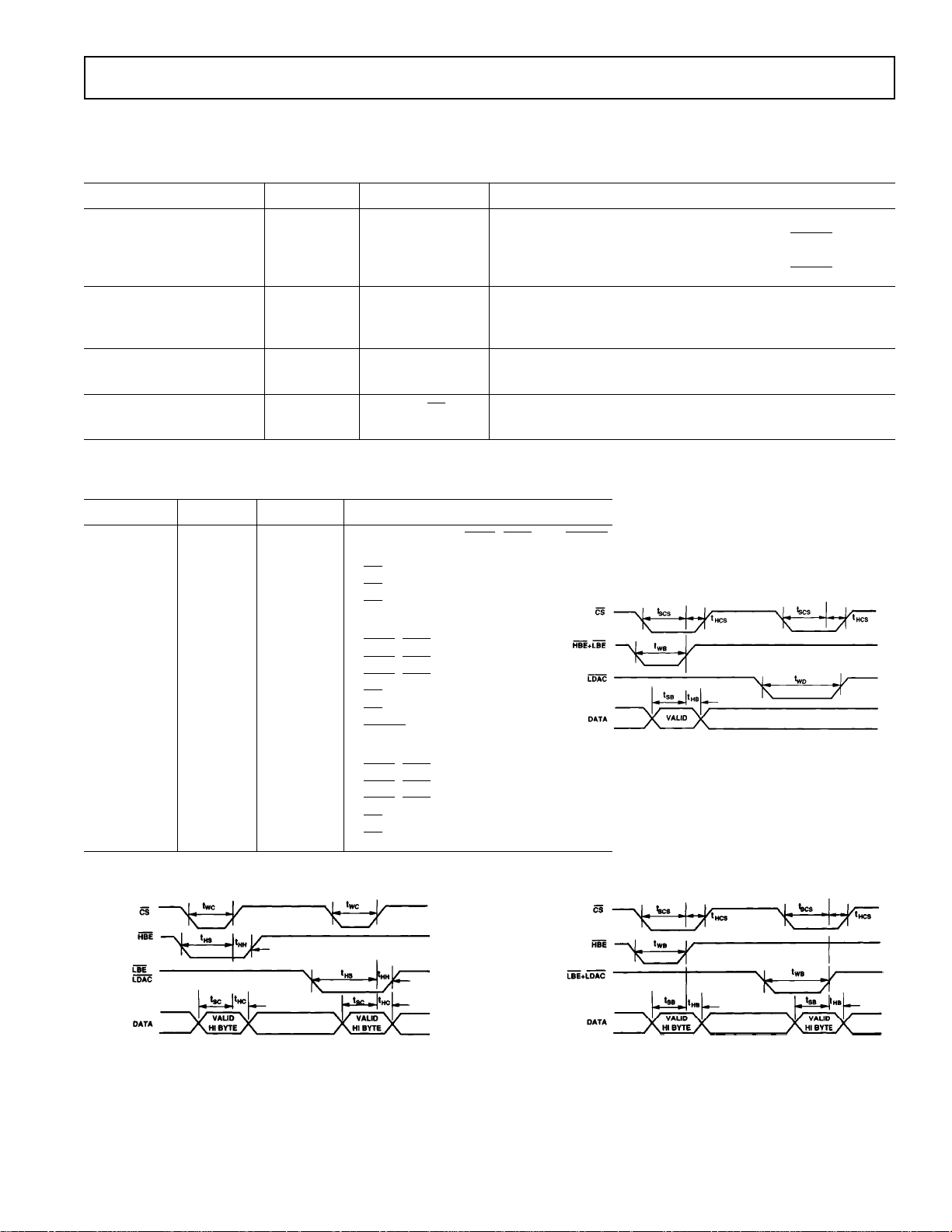
TIMING CHARACTERISTICS
(+VS = +12 V, –VS = –12 V, VIH = 2.4 V, VIL = 0.4 V,T
Parameter Limit Units Test Conditions/Comments
Case A 150 ns Pulse on HBE, LBE, and LDAC
T
= 140 ns min, THH = 10 ns min
t
t
t
WC
SC
HC
120 ns min CS Pulse Width
60 ns min CS Data Setup Time
20 ns min CS Data Hold Time
HS
Case B None
t
WB
t
SB
t
HB
t
SCS
t
HCS
t
WD
Case C None
t
WB
t
SB
t
HB
t
SCS
t
HCS
70 ns min HBE, LBE Pulse Width
80 ns min HBE, LBE Data Setup Time
20 ns min HBE, LBE Data Hold Time
120 ns min CS Setup Time
10 ns min CS Hold Time
120 ns min LDAC Pulse Width
Figure 2a. AD569 Timing Diagram – Case B
120 ns min HBE, LBE Pulse Width
80 ns min HBE, LBE Data Setup Time
20 ns min HBE, LBE Data Hold Time
120 ns min CS Setup Time
10 ns min CS Hold Time
and 0FFFH (worst-case
H
and –V
OUT
MIN
to T
MAX
REF
)
REV. A
Figure 1. AD569 Timing Diagram – Case A
Figure 2b. AD569 Timing Diagram – Case C
–3–
Page 4
AD569
WARNING!
ESD SENSITIVE DEVICE
ABSOLUTE MAXIMUM RATINGS*
(TA = +25°C unless otherwise noted)
+VS (Pin 1) to GND (Pin 18) . . . . . . . . . . . . . . +18 V, –0.3 V
–V
(Pin 28) to GND (Pin 18) . . . . . . . . . . . . . . –18 V, +0.3 V
S
+V
(Pin 1) to –VS (Pin 28) . . . . . . . . . . . . . . . +26.4 V, –0.3 V
S
Digital Inputs
(Pins 4-14, 19-27) to GND (Pin 18) . . . . . . . . . +V
+V
Force (Pin 3) to +V
REF
–V
Force (Pin 15) to –V
REF
V
Force (Pins 3, 15) to GND (Pin 18) . . . . . . . . . . . . . ±V
REF
V
Sense (Pins 2, 16) to GND (Pin 18) . . . . . . . . . . . . . ±V
REF
V
(Pin 17) . . . . . . . . . . . . . . . . . . Indefinite Short to GND
OUT
Sense (Pin 2) . . . . . . . . ±16.5 V
REF
Sense (Pin 16) . . . . . . . ±16.5 V
REF
. . . . . . . . . . . . . . . . . . . . . . . . Momentary Short to +V
, –0.3 V
S
–V
S,
Power Dissipation (Any Package) . . . . . . . . . . . . . . . 1000 mW
Operating Temperature Range
Commercial Plastic (JN, KN, JP, KP Versions) 0°C to +70°C
Industrial Ceramic (AD, BD Versions) . . . . –25°C to +85°C
Extended Ceramic (SD Versions) . . . . . . . –55°C to +125°C
Storage Temperature . . . . . . . . . . . . . . . . . . . –65°C to +150°C
Lead Temperature Range (Soldering, 10 secs) . . . . . . . +300°C
*Stresses above those listed under “Absolute Maximum Ratings” may cause
permanent damage to the device. This is a stress rating only and functional
S
operation of the device at these or any other conditions above those indicated in the
S
operational sections of this specification is not implied. Exposure to absolute
maximum rating conditions for extended periods may affect device reliability.
S
ESD SENSITIVITY
The AD569 features input protection circuitry consisting of large “distributed” diodes and polysilicon
series resistors to dissipate both high-energy discharges (Human Body Model) and fast, low-energy
pulses (Charged Device Model). Per Method 3015.2 of MIL-STD-883C, the AD569 has been
classified as a Category A device.
Proper ESD precautions are strongly recommended to avoid functional damage or performance
degradation. Charges as high as 4000 volts readily accumulate on the human body and test equipment
and discharge without detection. Unused devices must be stored in conductive foam or shunts, and
the foam should be discharged to the destination socket before devices are removed. For further
information on ESD precautions, refer to Analog Devices’ ESD Prevention Manual.
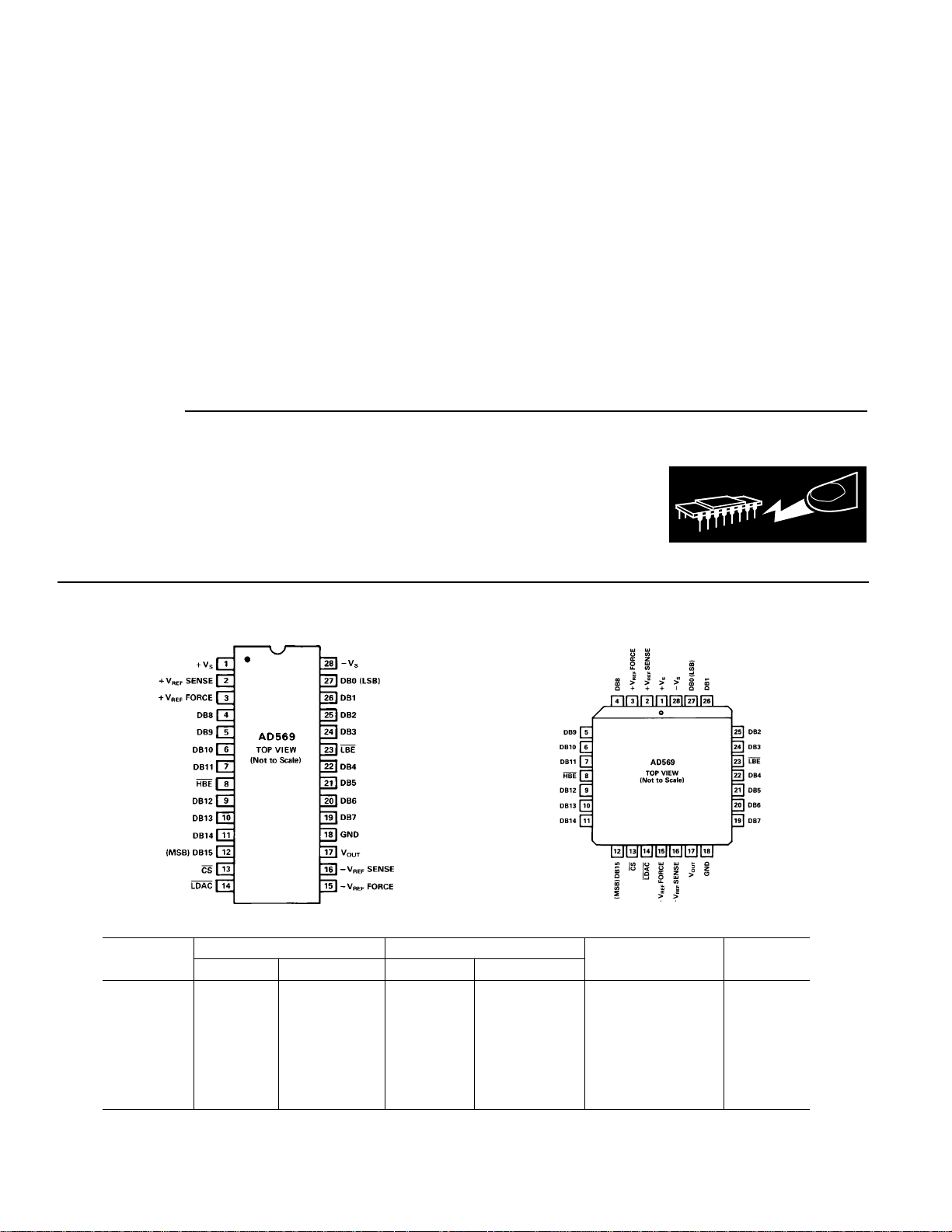
PIN DESIGNATIONS
ORDERING GUIDE
Integral Nonlinearity Differential Nonlinearity Temperature Package
+258CT
MIN–TMAX
+258CT
MIN–TMAX
Range Option
2
Model
1
AD569JN ±0.04% ±0.04% ±1 LSB ±1 LSB 0°C to +70°C N-28
AD569JP ±0.04% ±0.04% ±1 LSB ±1 LSB 0°C to +70°C P-28A
AD569KN ±0.024% ±0.024% ±1/2 LSB ±1 LSB 0°C to +70°C N-28
AD569KP ±0.024% ±0.024% ±1/2 LSB ±1 LSB 0°C to +70°C P-28A
AD569AD ±0.04% ±0.04% ±1 LSB ±1 LSB –25°C to +85°C D-28
AD569BD ±0.024% ±0.024% ±1/2 LSB ±1 LSB –25°C to +85°C D-28
AD569SD ±0.04% ±0.04% ±1 LSB ±1 LSB –55°C to +125°C D-28
NOTES
1
For details on grade and package offerings screened in accordance with MIL-STD-883, refer to the Analog Devices Military Products Databook
or current AD569/883B data sheet.
2
D = Ceramic DIP; N = Plastic DIP; P = Plastic Leaded Chip Carrier.
–4–
REV. A
Page 5

FUNCTIONAL DESCRIPTION
The AD569 consists of two resistor strings, each of which is divided into 256 equal segments (see Figure 3). The 8 MSBs of
the digital input word select one of the 256 segments on the first
string. The taps at the top and bottom of the selected segment
are connected to the inputs of the two buffer amplifiers A1 and
A2. These amplifiers exhibit extremely high CMRR and low
bias current, and thus accurately preserve the voltages at the top
and bottom of the segment. The buffered voltages from the segment endpoints are applied across the second resistor string,
where the 8LSBs of the digital input word select one of the 256
taps. Output amplifier A3 buffers this voltage and delivers it to
the output.
Buffer amplifiers A1 and A2 leap-frog up the first string to preserve monotonicity at the segment boundaries. For example,
when increasing the digital code from 00FF
to 0100H, (the first
H
segment boundary), A1 remains connected to the same tap on
the first resistor, while A2 jumps over it and is connected to the
tap which becomes the top of the next segment. This design
guarantees monotonicity even if the amplifiers have offset voltages. In fact, amplifier offset only contributes to integral linearity error.
CAUTION
It is generally considered good engineering practice to avoid
inserting integrated circuits into powered-up sockets. This
guideline is especially important with the AD569. An empty,
powered-up socket configures external buffer amplifiers in an
open-loop mode, forcing their outputs to be at the positive or
AD569
Figure 3. AD569 Block Diagram
negative rail. This condition may result in a large current surge
between the reference force and sense terminals. This current
surge may permanently damage the AD569.
ANALOG CIRCUIT DETAILS
Definitions
LINEARITY ERROR: Analog Devices defines linearity error as
the maximum deviation of the actual, adjusted DAC output
from the ideal output (a straight line drawn from 0 to FS–1LSB)
for any bit combination. The AD569’s linearity is primarily limited by resistor uniformity in the first divider (upper byte of
16-bit input). The plot in Figure 4 shows the AD569’s typical
linearity error across the entire output range to be within
±0.01% of full scale. At 25°C the maximum linearity error for
the AD569JN, AD and SD grades is specified to be ±0.04%,
and ±0.024% for the KN and BD versions.
Figure 4. Typical Linearity
MONOTONICITY: A DAC is monotonic if the output either
increases or remains constant for increasing digital inputs. All
versions of the AD569 are monotonic over their full operating
temperature range.
DIFFERENTIAL NONLINEARITY: DNL is the measure of
the change in the analog output, normalized to full scale, associated: with a 1 LSB change in the digital input code. Monotonic
behavior requires that the differential linearity error be less than
1 LSB over the temperature range of interest. For example, for a
±5 V output range, a change of 1 LSB in digital input code
should result in a 152 µV change in the analog output (1 LSB =
10 V/65,536). If the change is actually 38 µV, however, the dif-
ferential linearity error would be –114 µV, or –3/4 LSB. By leap-
frogging the buffer amplifier taps on the first divider, a typical
AD569 keeps DNL within ±38 µV (±1/4 LSB) around each of
the 256 segment boundaries defined by the upper byte of the input word (see Figure 5). Within the second divider, DNL also
typically remains less than ±38 µV as shown in Figure 6. Since
the second divider is independent of absolute voltage, DNL is
the same within the rest of the 256 segments.
OFFSET ERROR: The difference between the actual analog
output and the ideal output (–V
), with the inputs loaded with
REF
all zeros is called the offset error. For the AD569, Unipolar Offset is specified with 0 V applied to –V
specified with –5 V applied to –V
adjusting the voltage applied to the –V
and Bipolar Offset is
REF
. Either offset is trimmed by
REF
terminals.
REF
BIPOLAR ZERO ERROR: The deviation of the analog output
from the ideal half-scale output of 0.0000 V when the inputs are
loaded with 8000
is called the Bipolar Zero Error. For the
H
AD569, it is specified with ±5 V applied to the reference
terminals.
REV. A
–5–
Page 6

AD569
Figure 5. Typical DNL at Segment Boundary Transitions
a. Segment 1
b. Segment 256
Figure 6. Typical DNL Within Segments
MULTIPLYING FEEDTHROUGH ERROR: This is the error
due to capacitive feedthrough from the reference to the output
with the input registers loaded with all zeroes.
FULL-SCALE ERROR: The AD569’s voltage dividing architecture gives rise to a fixed full-scale error which is independent
of the reference voltage. This error is trimmed by adjusting the
voltage applied to the +V
DIGITAL-TO-ANALOG GLITCH IMPULSE: The charge injected into the analog output when a new input is latched into
the DAC register gives rise to the Digital-to-Analog Glitch
Impulse.
terminals.
REF
Glitches can be due to either time skews between the input bits
or charge injection from the internal switches. Glitch Impulse
for the AD569 is mainly due to charge injection, and is measured with the reference connections tied to ground. It is specified as the area of the glitch in nV-secs.
TOTAL ERROR: The worst-case Total Error is the sum of the
fixed full-scale and offset errors and the linearity error.
POWER SUPPLY AND REFERENCE VOLTAGE RANGES
The AD569 is specified for operation with ± 12 volt power
supplies. With ±10% power supply tolerances, the maximum
reference voltage range is ± 5 volts. Reference voltages up to
±6 volts can be used but linearity will degrade if the supplies
approach their lower limits of ± 10.8 volts (12 volts - 10%).
If ±12 volt power supplies are unavailable in the system, several
alternative schemes may be used to obtain the needed supply
voltages. For example, in a system with ± 15 V supplies, a single
Zener diode can be used to reduce one of the supplies to 9 volts
with the remaining one left at 15 volts. Figure 7a illustrates this
scheme. A 1N753A or equivalent diode is an appropriate choice
for the task. Asymmetrical power supplies can be used since the
AD569’s output is referenced to –V
only and thus floats
REF
relative to logic ground (GND, Pin 18). Assuming a worst-case
±1.5 volt tolerance on both supplies (10% of 15 volts), the
maximum reference voltage ranges would be +6 and –2 volts for
+V
= +15 V and VS = –9 V, and +2 to –8 volts for +VS = 9 V
S
and –V
= –15 V .
S
Alternately, two 3 V Zener diodes or voltage regulators can be
used to drop each ±15 volt supply to ±12 volts, respectively. In
Figure 7b, 1N746A diodes are a good choice for this task.
A third method may be used if both ± 15 volt and ±5 volt supplies are available. Figure 7c shows this approach. A combination of +V
range of 0 to 6 volts, while supplies of +V
= +15 V and –VS = –5 V can support a reference
S
= +5 V and –VS =
S
–15 V can support a reference range of 0 to –8 volts. Again,
10% power supply tolerances are assumed.
NOTE: Operation with +V
= +5 V alters the input latches’ op-
S
erating conditions causing minimum write pulse widths to extend to 1 µs or more. Control signals
CS, HBE, LBE, and
LDAC should, therefore, be tied low to render the latches trans-
parent.
No timing problems exist with operation at +V
–V
= –15 V. However, 10% tolerances on these supplies gener-
S
ate a worst-case condition at –V
(assuming +V
is derived from a +15 V supply). Under these
S
= –16.5 V and +VS = +7.5 V
S
= 9 V and
S
conditions, write pulse widths can stretch to 200 ns with similar
degradation of data setup and hold times. However, ±0.75 V
tolerances (±5%) yield minimal effects on digital timing with
write pulse widths remaining below 100 ns.
Finally, Figure 7d illustrates the use of the combination of an
AD588 and AD569 in a system with ± 15 volt supplies. As
shown, the AD588 is connected to provide ±5 V to the reference inputs of the AD569. It is doing double-duty by simultaneously regulating the supply voltages for the AD569 through
the use of the level shifting Zeners and transistors. This scheme
utilizes the capability of the outputs of the AD588 to source as
well as sink current. Two other benefits are realized by using
this approach. The first is that the AD569 is no longer directly
connected to the system power supplies. Output sensitivity to
variations in those supplies is, therefore, eliminated. The second
–6–
REV. A
Page 7

AD569
benefit is that, should a Zener diode fail (a short circuit would
be the most likely failure), the supply voltage decreases. This
differs from the situation where the diode is used as a series
regulator. In that case, a failure would place the unregulated
supply voltage on the AD569 terminal.
a. Zener Regulates Negative Supply
b. Diodes Regulate Both Supplies
ANALOG CIRCUIT CONNECTIONS
The AD569 is intended for use in applications where high resolution and stability are critical. Designed as a multiplying D/A
converter, the AD569 may be used with a fixed dc reference or
an ac reference. V
voltages at +V
may be any voltage or combination of
REF
FORCE
and –V
that remain within the bounds
FORCE
set for reference voltages as discussed in the power supply range
section. Since the AD569 is a multiplying D/A converter, its
output voltage, V
, is proportional to the product of the digi-
OUT
tal input word and the voltage at the reference terminal. The
transfer function is V
OUT
= D·V
where D is the fractional bi-
REF
nary value of the digital word applied to the converter using
offset-binary coding. Therefore, the output will range from
–V
for a digital input code of all zeros (0000H) to +V
REF
an input code of all ones (FFFF
).
H
REF
for
For applications where absolute accuracy is not critical, the
simple reference connection in Figure 8 can be used. Using only
the reference force inputs, this configuration maintains linearity
and 16-bit monotonicity, but introduces small, fixed offset and
gain errors. These errors are due to the voltage drops across resistors R
and RB shown in Figure 9. With a 10 V reference
A
voltage, the gain and offset errors will range from 80 mV to
100 mV. Resistors R
and RB were included in the first resistor
A
string to avoid degraded linearity due to uneven current densities at the string’s endpoints. Similarly, linearity would degrade
if the reference voltage were connected across the reference
sense terminals. Note that the resistance between the force and
sense terminals cannot be measured with an ohmmeter; the layout of the thin-film resistor string adds approximately 4 kΩ of
resistance (R
) at the sense tap.
S
c. Use of ±15 V and ±5 V Supplies
d. AD588 Produces References and Supply Voltages
Figure 7. Power Supply Options
REV. A
Figure 8. Simple Reference Connection
For those applications in which precision references and high
accuracy are critical, buffer amplifiers are used at +V
–V
as shown in Figure 10 to force the voltage across resistors
REF
REF
and
R1 to R256. This insures that any errors induced by currents
flowing through the resistances of the package pins, bond wires,
aluminum interconnections, as well as R
and RB are mini-
A
mized. Suitable amplifiers are the AD517, AD OP07, AD OP27,
or the dual amplifier, the AD712. Errors will arise, however, as
the buffer amplifiers’ bias currents flow through R
(4 kΩ). If
S
the bias currents produce such errors, resistance can be inserted
at the noninverting terminal (R
) of the buffer amplifiers to
BC
compensate for the errors.
–7–
Page 8

AD569
Figure 9. MSB Resistor Divider
Figures 11, 12, and 13 show reference configurations for various
output ranges. As shown in Figure 11, the pin-programmable
AD588 can be connected to provides tracking ± 5 V outputs
with 1-3ppm/°C temperature stability. Buffer amplifiers are included for direct connection to the AD569. The optional gain
and balance adjust trimmers allow bipolar offset and full-scale
errors to be nulled. In Figure 12, the low-cost AD586 provides
Figure 10. Reference Buffer Amplifier Connections
+5 V reference. A dual op amp, the AD712, buffers the reference input terminals preserving the absolute accuracy of the
AD569. The optional noise-reduction capacitor and gain
adjust trimmer allow further elimination of errors. The lowcost AD584 offers 2.5 V, 5 V, 7.5 V, and 10 V options and
can be connected for ±5 V tracking outputs as shown in Figure
13. Again, an AD712 is used to buffer the reference input
terminals.
Figure 11. Ultralow Drift ±5 V Tracking Reference
Figure 12. Low-Cost ±5 V Reference
–8–
REV. A
Page 9

Figure 13. Low-Cost ±5 V Tracking Reference
AD569
MULTIPLYING PERFORMANCE
Figure 14 illustrates the gain and phase characteristics of the
AD569 when operated in the multiplying mode. Full-power
bandwidth is shown in Figure 14a and the corresponding phase
shift is shown in Figure 14b. Performance is plotted for both a
full-scale input of FFFF
and an input of 8080H. An input rep-
H
resents worst-case conditions because it places the buffer taps at
a. Bandwidth
the midpoints of both dividers. Figure 15 illustrates the
AD569’s ability to resolve 16-bits (where 1 LSB is 96 dB below
full scale) while keeping the noise floor below –130 dB with an
ac reference of 1 V rms at 200 Hz.
Multiplying feedthrough is due to capacitive coupling between
the reference inputs and the output. As shown in Figure 16,
a. Time Domain
b. Phase Shift
Figure 14. Full Power Multiplying Performance
REV. A
b. Frequency Domain
Figure 15. Multiplying Mode Performance (Input Code
)
0001
H
–9–
Page 10

AD569
under worst-case conditions (hex input code 0000), feedthrough
remains below –100 dB at ac reference frequencies up to 10 kHz.
Figure 16. Multiplying Feedthrough
BYPASSING AND GROUNDING RULES
It is generally considered good engineering practice to use bypass
capacitors on the device supply voltage pins and to insert small
valued resistors in the supply lines to provide a measure of decoupling between various circuits in a system. For the AD569, bypass
capacitors of at least 4.7 µF and series resistors of 10 Ω are recom-
mended. The supply voltage pins should be decoupled to Pin 18.
NOISE
In high-resolution systems, noise is often the limiting factor. A
16-bit DAC with a 10 volt span has an LSB size of 152 µV
(–96 dB). Therefore, the noise floor must remain below this
level in the frequency ranges of interest. The AD569’s noise
spectral density is shown in Figures 17 and 18. The lowband
noise spectrum in Figure 17 shows the 1/f corner frequency at
1.2 kHz and Figure 18 shows the wideband noise to be below
40 nV/Ï
Hz.
Figure 17. Lowband Noise Spectrum
DIGITAL CIRCUIT CONNECTIONS
The AD569’s truth table appears in Table I. The High Byte Enable (
HBE) and Low Byte Enable (LBE) inputs load the upper
and lower bytes of the 16-bit input when Chip Select (
valid (low). A similar strobe to Load DAC (
16-bit input into the DAC register and completes the DAC update. The DAC register can either be loaded with a separate
write cycle or synchronously with either of the 8-bit registers in
the first rank. A simultaneous update of several AD569s can be
achieved by controlling their
signal.
Table I. AD569 Truth Table
CS HBE LBE LDAC OPERATION
1 X X X No Operation
X 1 1 1 No Operation
0 0 1 1 Enable 8 MSBs of First Rank
0 1 0 1 Enable 8 LSBs of First Rank
0 1 1 0 Enable 16-Bit DAC Register
0 0 0 0 All Latches Transparent
All four control inputs latches are level-triggered and active low.
When the DAC register is loaded directly from a bus, the data at
the digital inputs will be reflected in the output any time
LDAC, LBE and HBE are low. Should this not be the desired
case, bring
data. Alternately, use a second write cycle to transfer the data to
the DAC register or delay the write strobe pulse until the appropriate data is valid. Be sure to observe the appropriate data
setup and hold times (see Timing Characteristics).
Whenever possible, the write strobe signal should be applied to
HBE and LBE with the AD569’s decoded address applied to
CS. A minimum pulse width of 60 ns at HBE and LBE allows
the AD569 to interface to the fastest microprocessors. Actually,
data can be latched with narrower pulses, but the data setup and
hold times must be lengthened.
16-Bit Microprocessor Interfaces
Since 16-bit microprocessors supply the AD569’s complete 16bit input in one write cycle, the DAC register is often unnecessary. If so, it should be made transparent by grounding
The DAC’s decoded address should be applied to
write strobe applied to
terface in Figure 19.
LDAC (or HBE or LBE) high before changing the
LDAC inputs with a single control
HBE and LBE as shown in the 68000 in-
LDAC) loads the
CS) is
CS,
LDAC.
CS, with the
Figure 18. Wideband Noise Spectrum
–10–
Figure 19. AD569/68000 Interface
REV. A
Page 11

a. Simple Interface
b. Fast Interface
Figure 20. 8-Bit Microprocessor Interface
8-Bit Microprocessor Interfaces
Since 8-bit microprocessors require two write cycles to provide
the AD569’s 16-bit input, the DAC register must be utilized. It
is most often loaded as the second byte enters the first rank of
latches. This synchronous load method, shown in Figure 20, requires
LDAC to be tied to either LBE or HBE, depending upon
the byte loading sequence. In either case, the propagation delay
through the first rank gives rise to longer timing requirements as
shown in Figure 2. If the DAC register (
separately using a third write cycle, the minimum write pulse on
LDAC is 70 ns, as shown in Figure 1.
Two basic methods exist for interfacing the AD569 to an 8-bit
microprocessor’s address and control buses. In either case, at
least one address line is needed to differentiate between the upper and lower bytes of the first rank (
LDAC) is controlled
HBE and LBE). The sim-
AD569
plest method involves applying the two addresses directly to
HBE and LBE and strobing the data using CS as shown in Fig-
ure 20a. However, the minimum pulse width on
with a minimum data setup time of 60 ns. If operation with a
shorter pulse width is required, the base address should be applied to
supply the
since the write pulse sees a propagation delay, the data still must
remain valid at least 20 ns after the rising edge of the delayed
write pulse.
OUTPUT SETTLING
The AD569’s output buffer amplifier typically settles to within
±0.001% FS of its final value in 3 µs for a 10 V step. Figure 21
shows settling for negative and positive full-scale steps with no
load applied. Capable of sourcing or sinking 5 mA, the output
buffer can also drive loads of 1 kΩ and 1000 pF without loss of
stability. Typical settling to 0.001% under these worst-case conditions is 4 µs, and is guaranteed to be a maximum of 6 µs. The
plots of Figure 21 were generated using the settling test procedure developed specifically for the AD569.
Subranging 16-Bit ADC
The subranging ADC shown in Figure 22 completes a conversion in less than 20 µs, including the sample-hold amplifier’s
sample time. The sample-hold amplifier is allocated 5 µs to
settle to 16 bits.
Before the first flash, the analog input signal is routed through
the AD630 at a gain of +1. The lower AD7820 quantizes the
signal to the 8-bit level within 1.4 µs, and the 8-bit result is
routed to the AD569 via a digital latch which holds the 8-bit
word for the AD569 and the output logic.
The AD569’s reference polarity is reversed so that a full-scale
output is –5 V and zero scale is 0 V, thereby subtracting an 8-bit
approximation from the original sampled signal. The residue
from the analog subtraction is then quantized by the second 8bit flash conversion to recover the 8 LSBs. Even though only the
AD569’s upper 8 MSBs are used, the AD569’s accuracy defines the A/D converter’s overall accuracy. Any errors are directly reflected in the output.
CS with an address line gated with the strobe signal to
HBE and LBE inputs (see Figure 20b). However,
CS is 70 ns
REV. A
a. Turn-On Settling
b. Turn-Off Settling
Figure 21. Full-Scale Output Settling
–11–
Page 12

AD569
Preceding the second flash, the residue signal must be amplified
by a factor of 256. The OP37 provides a gain of 25.6 and the
AD630 provides another gain of 10. In this case, the AD630
acts as a gain element as well as a channel control switch. The
second flash conversion yields a 9-bit word. This provides one
extra bit of overlap for digital correction of any errors that occurred in the first flash. The correction bit is digitally added to
the first flash before the entire 16-bit output is strobed into the
output register.
C949a–12–8/87
28-Pin Ceramic DIP (D)
Figure 22. 16-Bit Subranging ADC
OUTLINE DIMENSIONS
Dimensions shown in inches and (mm).
28-Pin Plastic DIP (N)
28-Pin Plastic Leaded Chip Carrier (P)
PRINTED IN U.S.A.
–12–
REV. A
 Loading...