

Page 1
Octal, 12-14-16 Bit Dac with 10ppm/°C Max
On-Chip Reference in 14-Lead TSSOP
Preliminary Technical Data
FEATURES
Low Power Smallest Pin compatible Octal DACs
AD5668: 16 Bits
AD5648: 14 Bits
AD5628: 12 Bits
14/16-Lead TSSOP Package
On-chip 1.25/2.5V, 10ppm/°C Reference
Power-Down to 200 nA @ 5V, 50 nA @ 3V
3V/5V Power Supply
Guaranteed Monotonic by Design
Power-On-Reset to Zero/Midscale
Three Power-Down Functions
Hardware /LDAC and /CLR functions
Rail-to-Rail Operation
APPLICATIONS
ProcessControl
Data Acquisition Systems
Portable Battery Powered Instruments
Digital Gain and Offset Adjustment
Programmable Voltage and Current Sources
GENERAL DESCRIPTION
The AD5628/48/68 family of devices are low power, octal, 1214-16-bit buffered voltage-out DACs. All devices operate from
a single +2.7V to +5.5V, and are guaranteed monotonic by
design.
The AD5628/48/68 have an on-chip reference with an internal
gain of two. The AD56x8-1 has a 1.25V 10ppm/°C max
reference and the AD56x8-2,-3 have a 2.5V 10ppm/°C max
reference. The on-board reference is off at power-up allowing
the use of an external reference. The internal reference is
turned on by writing to the DAC. The part incorporates a
power-on-reset circuit that ensures that the DAC output
powers up to zero volts (AD56x8-1,-2/) or midscale (AD5668-
3) and remains there until a valid write takes place. The part
contains a power-down feature that reduces the current
consumption of the device to 200nA at 5V and provides
software selectable output loads while in power-down mode for
any or all DACs channels.
AD5628/AD5648/AD5668
Programmable Attenuators
V
I
NPUT
REGISTER
I
NPUT
REGISTER
I
NPUT
REGISTER
I
NPUT
REGISTER
I
NPUT
REGIS-
TER
I
NPUT
REGISTER
I
NPUT
REGISTER
I
NPUT
REGISTER
POWER-ON
DD
REGISTER
REGISTER
REGISTER
REGISTER
REGISTER
REGISTER
REGISTER
RESET
SCLK
SYNC
DIN
*RU-16 PACKAGE ONLY
AD5628/AD5648/AD5668
LDAC
INTERFACE
LOGIC
LDAC*
CLR*
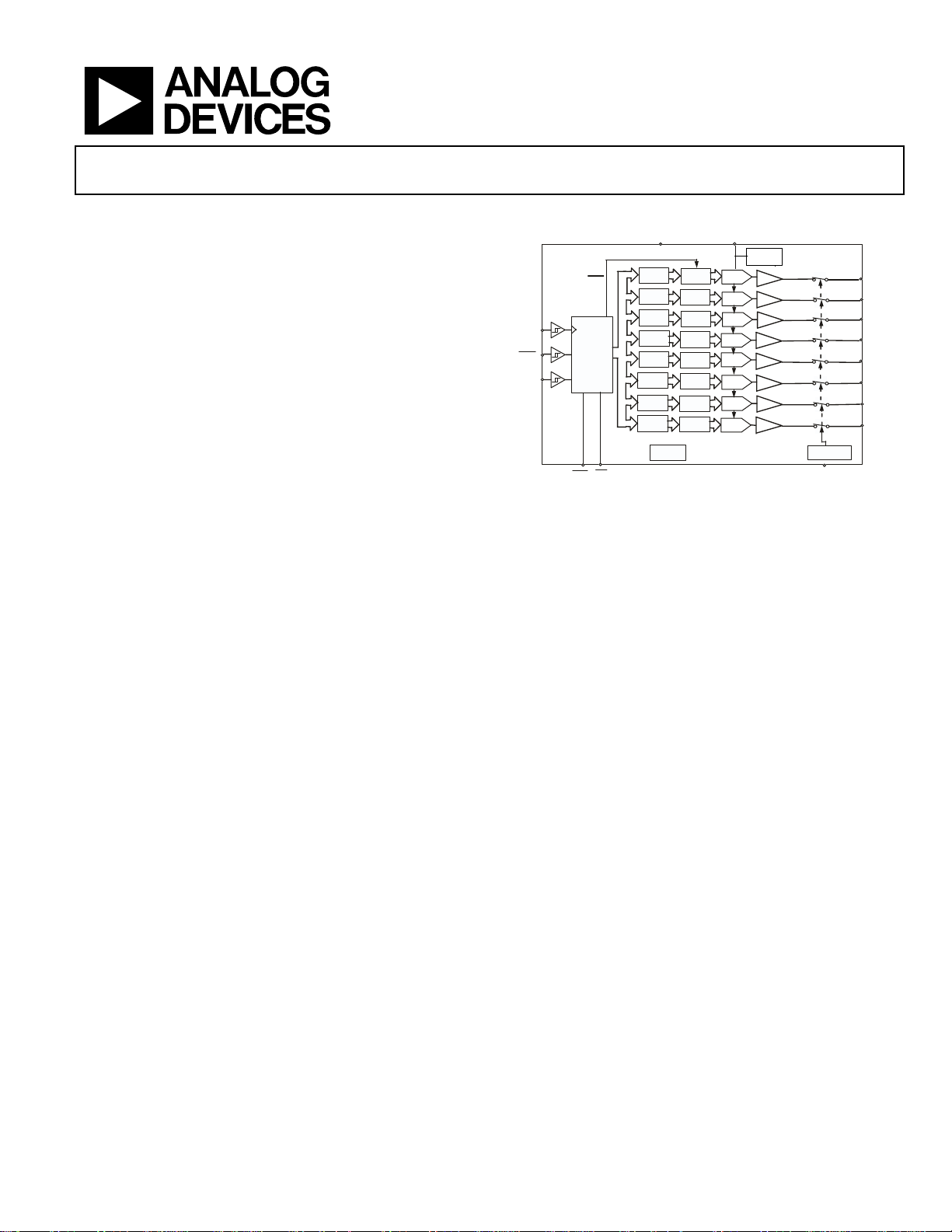
Figure 1. Functional Block Diagram
The outputs of all DACs may be updated simultaneously using
the /LDAC function, with the added functionality of selecting
through software any number of DAC channels to synchronize.
There is also an asynchronous active low /CLR that clears all
DACs to a software selectable code - 0 V, midscale or fullscale .
The AD5628/48/68 utilizes a versatile three-wire serial
interface that operates at clock rates up to 50 MHz and is
compatible with standard SPI™, QSPI™, MICROWIRE™ and
DSP interface standards. Its on-chip precision output amplifier
allows rail-to-rail output swing to be achieved.
PRODUCT HIGHLIGHTS
1. Octal 12/14/16-Bit DAC
2. On-chip 1.25/2.5V, 10ppm/°C max Reference.
3. Available in 14/16-lead TSSOP package.
4. Power-On-Reset to Zero volts or Midscale.
5. Power-down capability. When powered down, the
DAC typically consumes 50nA at 3V and 200nA at 5V.
DAC
DAC
DAC
D
AC
REGISTER
D
AC
D
AC
D
AC
D
AC
V
STRING
DAC A
STRING
DAC B
STRING
DAC C
STRING
DAC D
STRING
DAC E
STRING
DAC F
STRING
DAC G
STRING
DAC H
REF
1.25/2.5V
Ref
BUFFER
BUFFER
BUFFER
BUFFER
BUFFER
BUFFER
BUFFER
BUFFER
POWER-DOWN
GND
LOGIC
V
A
OUT
V
B
OUT
V
C
OUT
V
D
OUT
V
E
OUT
V
F
OUT
V
G
OUT
V
H
OUT
Rev. PrB
Information furnished by Analog Devices is believed to be accurate and reliable.
However, no responsibility is assumed by Analog Devices for its use, nor for any
infringements of patents or other rights of third parties that may result from its use.
Specifications subject to change without notice. No license is granted by implication
or otherwise under any patent or patent rights of Analog Devices. Trademarks and
registered trademarks are the property of their respective owners.
One Technology Way, P.O. Box 9106, Norwood, MA 02062-9106, U.S.A.
Tel: 781.329.4700 www.analog.com
Fax: 781.326.8703 © 2005 Analog Devices, Inc. All rights reserved.
Page 2

AD5628/AD5648/AD5668
Rev. PrB | Page 2 of 24
TABLE OF CONTENTS
Features.......................................................................................... 1
Applications................................................................................... 1
General Description..................................................................... 1
Product Highlights....................................................................... 1
AD5628/AD5648/AD5668–Specifications ................................... 3
Timing Characteristics..................................................................... 9
Pin Configuration and Function Descriptions........................... 10
Absolute Maximum Ratings.......................................................... 11
ESD Caution................................................................................ 11
Terminology ................................................................................ 12
REVISION HISTORY
Preliminary Technical Data
AD5628/AD5648/AD5668–Typical Performance
Characteristics ................................................................................ 14
General Description................................................................... 17
Serial Interface............................................................................ 17
Microprocessor Interfacing............................................................
Applications .....................................................................................
Outline Dimensions....................................................................... 24
Ordering Guide ...............................................................................
Revision 0: Initial Version
Rev.PrB | Page 2 of 25
Page 3
Preliminary Technical Data
Rev. PrB | Page 3 of 24
AD5628/AD5648/AD5668
AD5628/AD5648/AD5668–SPECIFICATIONS
(VDD = +4.5 V to +5.5 V; RL = 2 kΩ to GND; CL = 200 pF to GND; External REFIN = VDD; all specifications T
noted)
Table 1.
A Grade
B Version
Parameter Min Typ Max Unit
STATIC PERFORMANCE
3,4
Conditions/Comments
1,2
AD5628
Resolution 12 Bits
Relative Accuracy ±0.5 ±6 LSB See Figure 4
Differential Nonlinearity ±1 LSB Guaranteed Monotonic by Design. See Figure 5.
AD5648
Resolution 14 Bits
Relative Accuracy ±2 ±8 LSB See Figure 4
Differential Nonlinearity ±1 LSB Guaranteed Monotonic by Design. See Figure 5.
AD5668
Resolution 16 Bits
Relative Accuracy ±32 LSB See Figure 4
Differential Nonlinearity ±1 LSB Guaranteed Monotonic by Design. See Figure 5.
Load Regulation 2 LSB/mA
VDD=Vref=5V, Midscale
sourcing/sinking
Zero Code Error +1 +9 mV All Zeroes Loaded to DAC Register. See Figure 8.
Zero Code Error Drift3 ±20 µV/°C
Full-Scale Error -0.15 -1.25 % of FSR All Ones Loaded to DAC Register. See Figure 8.
Gain Error ±1.5 % of FSR
Gain Temperature Coefficient ±5 ppm of FSR/°C
Offset Error ±1 ±9 mV
Offset Temperature Coefficient 1.7 µV/°C
DC Power Supply Rejection Ratio6
DC Crosstalk6 (Ext Ref)
DC Crosstalk6 (Int Ref)
10
4.5
10
20
4.5
20
–80
dB VDD ±10%
µV
µV/mA
µV
µV
µV/mA
µV
RL = 2 k. to GND or VDD
Due to Load current change
Due to Powering Down (per channel)
RL = 2 k. to GND or VDD
Due to Load current change
Due to Powering Down (per channel)
OUTPUT CHARACTERISTICS6
Output Voltage Range 0 VDD V
Capacitive Load Stability 2 pF RL=∞
10 pF RL=2 kΩ
DC Output Impedance 0.5 Ω
Short Circuit Current 30 mA VDD=+5V
Power-Up Time 4 µs Coming out of Power-Down Mode. VDD=+5V
1
Temperature ranges are as follows: B Version: -40°C to +125°C, typical at 25°C.
2
Linearity calculated using a reduced code range of 485 to 64714. Output unloaded.
3
DC specifications tested with the outputs unloaded unless stated otherwise.
4
Linearity is tested using a reduced code range: AD5628 (Code 48 to Code 4047), AD5648 (Code / to Code /), and AD5668 (Code 485 to 64714).
6
Guaranteed by design and characterization; not production tested.
8
Interface inactive. All DACs active. DAC outputs unloaded.
9
All eight DACs powered down.
Specifications subject to change without notice.
MIN
to T
unless otherwise
MAX
Iout=0mA to 1mA
Rev. PrB| Page 3 of 25
Page 4
AD5628/AD5648/AD5668
Rev. PrB | Page 4 of 24
A Grade
Parameter Min Typ Max Unit
REFERENCE INPUTS3
Reference Input voltage
Reference Current 35 45 µ A V
Reference Input Range 0 VDD
Reference Input Impedance 14.6
REFERENCE OUTPUT
Output Voltage
AD5628/AD5648/AD5668x-2/3 2.495 2.5 2.505 V
Reference TC ±10 ppm/°C
Reference Output Impedance 2
LOGIC INPUTS3
Input Current ±1 µA
V
, Input Low Voltage 0.8 V VDD=+5 V
INL
V
, Input High Voltage 2 V VDD=+5 V
INH
Pin Capacitance 3 pF
POWER REQUIREMENTS
VDD 4.5 5.5 V All Digital Inputs at 0 or VDD
IDD (Normal Mode)8 DAC Active and Excluding Load Current
VDD=4.5 V to +5.5 V 2 4 mA VIH=VDD and VIL=GND
IDD (All Power-Down Modes)9
VDD=4.5 V to +5.5 V 0.2 1 µA VIH=VDD and VIL=GND
POWER EFFICIENCY
I
89 % I
OUT/IDD
VDD
V ±1% for specified performance
kΩ
kΩ
Preliminary Technical Data
B Version
Conditions/Comments
REF
Per DAC channel
LOAD
1,2
= VDD = +5.5V (per DAC channel)
=2 mA, VDD=+5 V
Rev.PrB | Page 4 of 25
Page 5
Preliminary Technical Data
Rev. PrB | Page 5 of 24
1
AC CHARACTERISTICS
specifications T
MIN
to T
unless otherwise noted)
MAX
(VDD = +4.5 V to +5.5 V; RL = 2 kΩ to GND; CL = 200 pF to GND; External REFIN = VDD; all
AD5628/AD5648/AD5668
Parameter2 Min Typ Max Unit
Output Voltage Settling Time
AD5628 6 8 µs ¼ to ¾ scale settling to ±2LSB
AD5648 7 9 µs ¼ to ¾ scale settling to ±2LSB
AD5668 8 10 µs ¼ to ¾ scale settling to ±2LSB
Settling Time for 1LSB Step
Slew Rate 1.5 V/µs
Digital-to-Analog Glitch Impulse 5 nV-s 1 LSB Change Around Major Carry. See Figure 21.
Channel –to-Channel Isolation 100 dB
Digital Feedthrough 0.1 nV-s
Digital Crosstalk 0.5 nV-s
Analog Crosstalk 1 nV-s
DAC-to-DAC Crosstalk 3 nV-s
Multiplying Bandwidth 200 kHz VREF = 2V ± 0.1 V p-p.
Total Harmonic Distortion -80 dB VREF = 2V ± 0.1 V p-p. Frequency = 10kHz
Output Noise Spectral Density 120 nV/√Hz DAC code=8400H, 1kHz
100 nV/√Hz DAC code=8400H, 10kHz
Output Noise 15
1
µVp-p
B Version
Conditions/Comments
0.1Hz to 10Hz;
NOTES
1Guaranteed by design and characterization; not production tested.
2See the Terminology section.
3Temperature range (Y Version): –40°C to +125°C; typical at +25°C.
Specifications subject to change without notice.
Rev. PrB| Page 5 of 25
Page 6
AD5628/AD5648/AD5668
Rev. PrB | Page 6 of 24
Preliminary Technical Data
AD5628/AD5648/AD5668–SPECIFICATIONS
(VDD = +2.7 V to +3.6 V; RL = 2 kΩ to GND; CL = 200 pF to GND; External REFIN = V
noted)
Table 2.
A Grade
Parameter Min Typ Max Unit
STATIC PERFORMANCE
AD5628
Resolution 12 Bits
Relative Accuracy ±0.5 ±6 LSB See Figure 4
Differential Nonlinearity ±1 LSB
AD5648
Resolution 14 Bits
Relative Accuracy ±2 ±8 LSB See Figure 4
Differential Nonlinearity ±1 LSB
AD5668
Resolution 16 Bits
Relative Accuracy ±32 LSB See Figure 4
Differential Nonlinearity ±1 LSB
Load Regulation 4 LSB/mA
Zero Code Error +1 +9 mV
Zero Code Error Drift1 ±20 µV/°C
Full-Scale Error -0.15 -1.25 % of FSR
Gain Error ±0.7 % of FSR
Gain Temperature Coefficient ±5 ppm of FSR/°C
Offset Error ±1 ±9 mV
Offset Temperature Coefficient 1.7 µV/°C
DC Power Supply Rejection Ratio6
DC Crosstalk6 (Ext Ref)
DC Crosstalk6 (Int Ref)
OUTPUT CHARACTERISTICS6
Output Voltage Range 0 VDD V
Capacitive Load Stability 2 pF RL=∞
10 pF RL=2 kΩ
DC Output Impedance 0.5 Ω
Short Circuit Current 30 mA VDD=+3V
Power-Up Time 5 µs Coming Out of Power-Down Mode. VDD=+3V
REFERENCE INPUTS3
Reference Input voltage
3,4
–80
10
4.5
10
20
4.5
20
V
DD
V ±1% for specified performance
dB VDD ±10%
µV
µV/mA
µV
µV
µV/mA
µV
; all specifications T
DD
B Version
Conditions/Comments
Guaranteed Monotonic by Design. See Figure
5.
Guaranteed Monotonic by Design. See Figure
5.
Guaranteed Monotonic by Design. See Figure
5.
VDD=Vref=3V, Midscale
sourcing/sinking
All Zeroes Loaded to DAC Register. See Figure
8.
All Ones Loaded to DAC Register. See Figure
8.
RL = 2 k. to GND or VDD
Due to Load current change
Due to Powering Down (per channel)
RL = 2 k. to GND or VDD
Due to Load current change
Due to Powering Down (per channel)
1,1
to T
MIN
unless otherwise
MAX
Iout=0mA to 7.5mA
Rev.PrB | Page 6 of 25
Page 7
Preliminary Technical Data
Rev. PrB | Page 7 of 24
AD5628/AD5648/AD5668
Reference Current 20 20 µ A V
= VDD = +3.6V (per DAC channel)
REF
Reference Input Range 0 VDD
Reference Input Impedance 14.6
kΩ
Per DAC channel
REFERENCE OUTPUT
Output Voltage
AD5628/AD5648/AD5668x-1 1.248 1.25 1.252 V
Reference TC ±10 ppm/°C
Reference Output Impedance 2
kΩ
LOGIC INPUTS3
Input Current ±1 µA
V
, Input Low Voltage 0.8 V VDD=+3 V
INL
V
, Input High Voltage 2 V VDD=+3 V
INH
Pin Capacitance 3 pF
POWER REQUIREMENTS
VDD 2.7 3.6 V All Digital Inputs at 0 or VDD
IDD (Normal Mode)8 DAC Active and Excluding Load Current
VDD=2.7 V to +3.6 V 2 4 mA VIH=VDD and VIL=GND
IDD (All Power-Down Modes)9
VDD=2.7 V to +3.6 V 0.2 1 µA VIH=VDD and VIL=GND
POWER EFFICIENCY
I
89 % I
OUT/IDD
=2 mA, VDD=+5 V
LOAD
AC CHARACTERISTICS1
(VDD = +2.7 V to +3.6 V; RL = 2 kΩ to GND; CL = 200 pF to GND; External REFIN = VDD; all specifications T
noted)
B Version
Parameter2 Min Typ Max Unit
Conditions/Comments
1
Output Voltage Settling Time
AD5628 6 8 µs ¼ to ¾ scale settling to ±2LSB
AD5648 7 9 µs ¼ to ¾ scale settling to ±2LSB
AD5668 8 10 µs ¼ to ¾ scale settling to ±2LSB
Settling Time for 1LSB Step
Slew Rate 1.5 V/µs
Digital-to-Analog Glitch Impulse 10 nV-s 1 LSB Change Around Major Carry. See Figure 21.
Channel –to-Channel Isolation 100 dB
Digital Feedthrough 0.5 nV-s
Digital Crosstalk 0.5 nV-s
Analog Crosstalk 1 nV-s
DAC-to-DAC Crosstalk 3 nV-s
Multiplying Bandwidth 200 kHz VREF = 2V ± 0.1 V p-p.
Total Harmonic Distortion -80 dB VREF = 2V ± 0.1 V p-p. Frequency = 10kHz
Output Noise Spectral Density 120 nV/√Hz DAC code=8400H, 1kHz
100 nV/√Hz DAC code=8400H, 10kHz
Output Noise 15
NOTES
1Guaranteed by design and characterization; not production tested.
2See the Terminology section.
3Temperature range (Y Version): –40°C to +125°C; typical at +25°C.
Specifications subject to change without notice.
µVp-p
0.1Hz to 10Hz;
MIN
to T
unless otherwise
MAX
Rev. PrB| Page 7 of 25
Page 8
Preliminary Technical Data
Rev. PrB | Page 8 of 24
AD5628/AD5648/AD5668
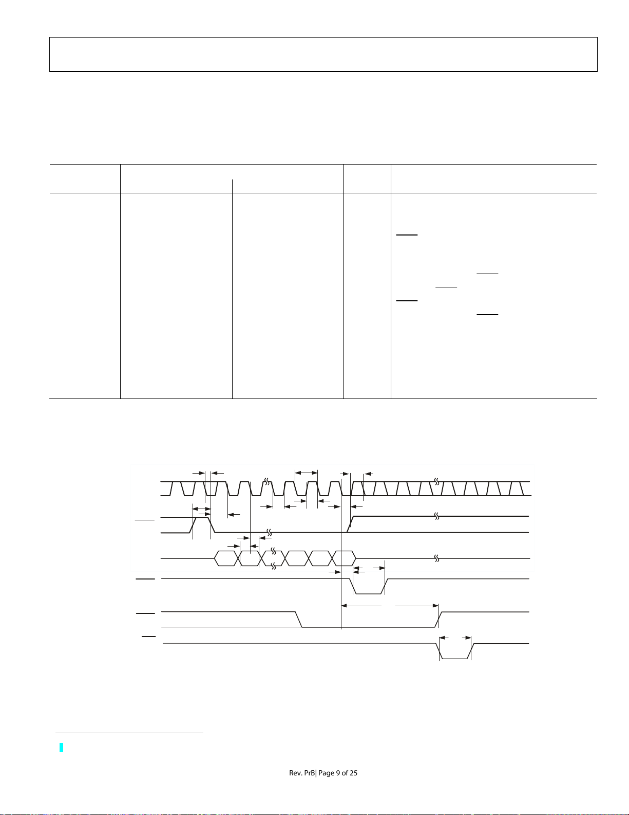
TIMING CHARACTERISTICS
All input signals are specified with tr = tf = 1 ns/V (10% to 90% of VDD) and timed from a voltage level of (VIL + VIH)/2.
See Figure 2.
= +2.7 V to +5.5 V; all specifications T
(V
DD
Limit at T
Parameter V
= 2.7 V to 3.6 V VDD= 3.6 V to 5.5 V Unit Conditions/Comments
DD
MIN
to T
MIN
unless otherwise noted)
MAX
, T
MAX
t1 1 20 20 ns min SCLK Cycle Time
t2 11 9 ns min SCLK High Time
t3 9 9 ns min SCLK Low Time
t4 13 13 ns min
SYNC
to SCLK Falling Edge Setup Time
t5 4 4 ns min Data Setup Time
t6 4 4 ns min Data Hold Time
t7 0 0 ns min
t8 25 20 ns min
t9 13 13 ns min
t10 0 0 ns min
t11 20 20 ns min
t12 20 20 ns min
SCLK Falling Edge to
Minimum
SYNC
SYNC
Rising Edge to SCLK Fall Ignore
SCLK Falling Edge to
LDAC Pulsewidth Low
SCLK Falling Edge to LDAC Rising Edge
SYNC
High Time
SYNC
Rising Edge
Fall Ignore
t13 20 20 ns min /CLR Pulse Width Low
t14 0 0 ns min
SCLK Falling Edge to LDAC Falling Edge
t15 tbd tbd ns min /CLR Pulse Activation Time (AD5380?)
t
10
SCLK
t
8
SYNC
DIN
LDAC1
LDAC2
CLR
NOTES
1. ASYNCHRONOUS LDAC UPDATE MODE.
2. SYNCHRONOUS LDAC UPDATE MODE.
DB31
t
4
t
5
1
3Maximum SCLK frequency is 50 MHz at VDD = +2.7 V to +5.5 V
t
1
t
t
3
t
6
2
Figure 2. Serial Write Operation
DB0
t
t14
t
9
7
t11
t12
t13
Rev. PrB| Page 9 of 25
Page 9

AD5628/AD5648/AD5668
Rev. PrB | Page 9 of 24
PIN CONFIGURATION AND FUNCTION DESCRIPTIONS
Preliminary Technical Data
V
V
V
V
SYNC
V
OUT
OUT
OUT
OUT
V
DD
REF
1
2
A
3
4
C
5
E
6
G
7
AD5628
AD5648
AD5668
TOP VIEW
(Not to Scale)
14
SCLK
13
DIN
12
GND
11
V
B
OUT
V
D
10
OUT
9
V
F
OUT
8
V
H
OUT
V
V
V
V
OUT
LDAC
SYNC
V
OUT
OUT
OUT
V
REF
DD
A
C
E
G
1
AD5628
2
AD5648
3
AD5668
4
TOP VIEW
(Not to Scale)
5
6
7
8
16
SCLK
15
DIN
14
GND
V
B
13
OUT
V
D
12
OUT
11
V
F
OUT
V
H
10
OUT
9
CLR
Figure 3. 14-Lead TSSOP (RU-14) Figure 4. 16-Lead TSSOP (RU-16)
Table 2. Pin Function Descriptions
Pin No. Mnemonic Function
1 /LDAC Pulsing this pin low allows any or all DAC registers to be updated if the input registers have new data.
This allows simultaneous update of all DAC outputs. Alternatively, this pin can be tied permanently
low.
2 /SYNC
Active Low-Control Input. This is the frame synchronization signal for the input data. When SYNC
goes low, it powers on the SCLK and DIN buffers and enables the input shift register. Data is
transferred in on the falling edges of the following 32 clocks. If SYNC is taken high before the 32nd
falling edge, the rising edge of SYNC acts as an interrupt and the write sequence is ignored by the
device.
3 VDD Power Supply Input. These parts can be operated from 2.5 V to 5.5 V, and the supply should be
decoupled with a 10 µF capacitor in parallel with a 0.1 µF capacitor to GND.
4 VOUTA Analog Output Voltage from DAC A. The output amplifier has rail-to-rail operation.
13 VOUTB Analog Output Voltage from DAC B. The output amplifier has rail-to-rail operation.
5 VOUTC Analog Output Voltage from DAC C. The output amplifier has rail-to-rail operation.
12 VOUTD Analog Output Voltage from DAC D. The output amplifier has rail-to-rail operation.
8 VREF Reference Input/Output Pin
9 /CLR
Active Low Control Input that Loads Software selectable code – Zero, midscale, fullscale - to All Input and
DAC Registers. Therefore, the outputs also go to selected code. Default clears the output to 0V.
6 VOUTE Analog Output Voltage from DAC E. The output amplifier has rail-to-rail operation.
11 VOUTF Analog Output Voltage from DAC F. The output amplifier has rail-to-rail operation.
7 VOUTG Analog Output Voltage from DAC G. The output amplifier has rail-to-rail operation.
10 VOUTH Analog Output Voltage from DAC H. The output amplifier has rail-to-rail operation.
14 GND Ground Reference Point for All Circuitry on the Part.
15 DIN Serial Data Input. This device has a 32-bit shift register. Data is clocked into the register on the falling
edge of the serial clock input.
16 SCLK Serial Clock Input. Data is clocked into the input shift register on the falling edge of the serial clock
input. Data can be transferred at rates up to 50 MHz.
Rev.PrB | Page 10 of 25
Page 10

Preliminary Technical Data
Rev. PrB | Page 10 of 24
AD5628/AD5648/AD5668
ABSOLUTE MAXIMUM RATINGS
V
to GND -0.3 V to VDD + 0.3 V
Stresses above those listed under Absolute Maximum Ratings
may cause permanent damage to the device. This is a stress
rating only; functional operation of the device at these or any
other conditions above those listed in the operational sections
of this specification is not implied. Exposure to absolute
maximum rating conditions for extended periods may affect
device reliability.
= +25°C unless otherwise noted)
(T
A
Parameter Rating
VDD to GND -0.3 V to +7 V
Digital Input Voltage to GND -0.3 V to VDD + 0.3 V
ESD CAUTION
ESD (electrostatic discharge) sensitive device. Electrostatic charges as high as 4000 V readily accumulate on the
human body and test equipment and can discharge without detection. Although this product features
proprietary ESD protection circuitry, permanent damage may occur on devices subjected to high energy
electrostatic discharges. Therefore, proper ESD precautions are recommended to avoid performance
degradation or loss of functionality.
OUT
Operating Temperature Range
Industrial (B Version) -40°C to +105°C
Storage Temperature Range -65°C to +150°C
Junction Temperature (TJ Max) +150°C
TSSOP Package
Power Dissipation (TJ Max-TA)/θJA
θJA Thermal Impedance 150.4°C/W
Lead Temperature, Soldering
Vapor Phase (60 sec) +215°C
Infrared (15 sec) +220°C
Rev. PrB| Page 11 of 25
Page 11

AD5628/AD5648/AD5668
Rev. PrB | Page 11 of 24
TERMINOLOGY
Relative Accuracy
For the DAC, relative accuracy or Integral Nonlinearity (INL) is a
measure of the maximum deviation, in LSBs, from a straight line
passing through the endpoints of the DAC transfer function. A
typical INL vs. code plot can be seen in Figure 2.
Differential Nonlinearity
Differential Nonlinearity (DNL) is the difference between the
measured change and the ideal 1 LSB change between any two
adjacent codes. A specified differential nonlinearity of ±1 LSB
maximum ensures monotonicity. This DAC is guaranteed
monotonic by design. A typical DNL vs. code plot can be seen in
Figure 3.
Offset Error
Offset error is a measure of the difference between VOUT
(actual) and VOUT (ideal) expressed in mV in the linear
region of the transfer function. Offset error is measured on
the AD5668 with Code 512 loaded into the DAC register.
This is a measure of the offset error of the DAC and the output
amplifier (see Figures 2 and 3). It can be negative or positive, and is
expressed in mV.
Zero-Code Error
Zero-code error is a measure of the output error when zero code
(0000Hex) is loaded to the DAC register. Ideally the output should
be 0 V. The zero-code error is always positive in the AD56x8
because the output of the DAC cannot go below 0 V. It is due to a
combination of the offset errors in the DAC and output amplifier.
Zero-code error is expressed in mV. A plot of zero-code error vs.
temperature can be seen in Figure 6.
Gain Error
This is a measure of the span error of the DAC. It is the deviation
in slope of the DAC transfer characteristic from ideal expressed as
a percent of the full-scale range.
Zero-Code Error Drift
This is a measure of the change in zero-code error with a change in
temperature. It is expressed in µV/°C.
Gain Error Drift
This is a measure of the change in gain error with changes in
temperature. It is expressed in (ppm of full-scale range)/°C.
Full-Scale Error
Full-scale error is a measure of the output error when full-scale
Preliminary Technical Data
code (FFFF Hex) is loaded to the DAC register. Ideally the output
should be VDD – 1 LSB. Full-scale error is expressed in percent of
full-scale range. A plot of full-scale error vs. temperature can be
seen in Figure 6.
Total Unadjusted Error
Total Unadjusted Error (TUE) is a measure of the output error
taking the various offset and gain errors into account. A typical
TUE vs. code plot can be seen in Figure 4.
Digital-to-Analog Glitch Impulse
Digital-to-analog glitch impulse is the impulse injected into the
analog output when the input code in the DAC register changes
state. It is normally specified as the area of the glitch in nV secs and
is measured when the digital input code is changed by 1 LSB at the
major carry transition (7FFF Hex to 8000 Hex). See Figure 19.
DC Power Supply Rejection Ratio (PSRR)
This indicates how the output of the DAC is affected by changes in
the supply voltage. PSRR is the ratio of the change in VOUT
to a change in VDD for full-scale output of the DAC. It is
measured in dB. VREF is held at 2 V and VDD is varied ±10%.
DC Crosstalk
This is the dc change in the output level of one DAC in response to
a change in the output of another DAC. It is measured with a full-
scale output change on one DAC while monitoring another DAC
kept at midscale. It is expressed in µV.
Reference Feedthrough
This is the ratio of the amplitude of the signal at the DAC output to
the reference input when the DAC output is not being updated
(i.e., LDAC is high). It is expressed in dB.
Channel-to-Channel Isolation
This is the ratio of the amplitude of the signal at the output of one
DAC to a sine wave on the reference input of another DAC. It is
measured in dB.
Digital Feedthrough
Digital feedthrough is a measure of the impulse injected into the
analog output of a DAC from the digital input pins of the device,
but is measured when the DAC is not being written to (SYNC held
high). It is specified in nV-s and is measured with a fullscale
change on the digital input pins, i.e., from all 0s to all 1s and vice
versa.
Digital Crosstalk
This is the glitch impulse transferred to the output of one DAC at
midscale in response to a full-scale code change (all 0s to all 1s and
vice versa) in the input register of another DAC. It is measured in
Rev.PrB | Page 12 of 25
Page 12

Preliminary Technical Data
Rev. PrB | Page 12 of 24
standalone mode and is expressed in nV-s.
AD5628/AD5648/AD5668
nV-s.
Analog Crosstalk
This is the glitch impulse transferred to the output of one DAC due
to a change in the output of another DAC. It is measured by
loading one of the input registers with a full-scale code change (all
0s to all 1s and vice versa) while keeping LDAC high. Then pulse
LDAC low and monitor the output of the DAC whose digital code
was not changed. The area of the glitch is expressed in nV-s.
DAC-to-DAC Crosstalk
This is the glitch impulse transferred to the output of one DAC due
to a digital code change and subsequent output change of another
DAC. This includes both digital and analog crosstalk. It is
measured by loading one of the DACs with a full-scale code change
(all 0s to all 1s and vice versa) with LDAC low and monitoring the
output of another DAC. The energy of the glitch is expressed in
Multiplying Bandwidth
The amplifiers within the DAC have a finite bandwidth. The
multiplying bandwidth is a measure of this. A sine wave on the
reference (with full-scale code loaded to the DAC) appears on the
output. The multiplying bandwidth is the frequency at which the
output amplitude falls to 3 dB below the input.
Total Harmonic Distortion
This is the difference between an ideal sine wave and its attenuated
version using the DAC. The sine wave is used as the reference for
the DAC, and the THD is a measure of the harmonics present on
the DAC output. It is measured in dB.
Rev. PrB| Page 13 of 25
Page 13

AD5628/AD5648/AD5668
Rev. PrB | Page 13 of 24
Preliminary Technical Data
AD5628/AD5648/AD5668–TYPICAL PERFORMANCE CHARACTERISTICS
Figure 4. Typical INL Plot
Figure 7. INL Error and DNL Error vs. Temperature
Figure 5. Typical DNL Plot
Figure 6. Typical Total Unadjusted Error Plot
Rev.PrB | Page 14 of 25
Figure 8. Zero-Scale Error and Full-Scale Error vs. Temperature
Figure 9. I
Histogram with VDD=3V and VDD=5V
DD
Page 14

Preliminary Technical Data
Rev. PrB | Page 14 of 24
AD5628/AD5648/AD5668
Figure 10. Source and Sink Current Capability with V
Figure 11. Source and Sink Current Capability with V
DD
DD
=3V
=5 V
Figure 13. Supply Current vs. Temperature
Figure 14. Supply Current vs. Supply Voltage
Figure 12. Supply Current vs. Code
Rev. PrB| Page 15 of 25
Figure 15. Power-Down Current vs. Supply Voltage
Page 15

AD5628/AD5648/AD5668
Rev. PrB | Page 15 of 24
Figure 16. Supply Current vs. Logic Input Voltage
Preliminary Technical Data
Figure 19. Power-On Reset to 0V
Figure 20. Exiting Power-Down (800 Hex Loaded)
Figure 17. Full-Scale Settling Time
Figure 18. Half-Scale Settling Time
Figure 21. Digital-to-Analog Glitch Impulse
Rev.PrB | Page 16 of 25
Page 16

Preliminary Technical Data
Rev. PrB | Page 16 of 24
GENERAL DESCRIPTION
D/A Section
The AD5628/AD5648/AD5668 DACs are fabricated on a
CMOS process. The architecture consists of a string DAC
followed by an output buffer amplifier. The parts include an
internal 1.25/2.5V, 10ppm/°C reference with an internal gain of
two. Figure 22 shows a block diagram of the DAC architecture.
V
DD
REF (+)
DAC REGISTER
Figure 22. DAC Architecture
Since the input coding to the DAC is straight binary, the ideal
output voltage is given by:
OUT
OUT
where D = decimal equivalent of the binary code that is loaded
to the DAC register;
0 - 4095 for AD5628 (12 bit)
0 - 16383 for AD5648 (14 bit)
0 - 65535 for AD5668 (16 bit)
N = the DAC resolution
RESISTOR
STRING
REF ()
GND
⎛
extVrefV
)(
×=
⎜
⎝
VrefV
(int)2
×∗=
OUTPUT
AMPLIFIER
(Gain=2)
D
⎞
⎟
^2
N
⎠
D
⎛
⎜
⎝
⎞
⎟
^2
N
⎠
V
OUT
AD5628/AD5648/AD5668
Figure 23. Resistor String
Resistor String
The resistor string section is shown in Figure 23. It is simply a
string of resistors, each of value R. The code loaded to the DAC
register determines at which node on the string the voltage is
tapped off to be fed into the output amplifier. The voltage is
tapped off by closing one of the switches connecting the string
to the amplifier. Because it is a string of resistors, it is
guaranteed monotonic.
Output Amplifier
The output buffer amplifier is capable of generating rail-to-rail
voltages on its output which gives an output range of 0 V to
. It is capable of driving a load of 2 kΩ in parallel with 1000
V
DD
pF to GND. The source and sink capabilities of the output
amplifier can be seen in Figure 10 and Figure 11. The slew rate
is 1.5 V/µs with a half-scale settling time of 8 µs with the output
unloaded.
SERIAL INTERFACE
The AD5628/AD5648/AD5668 has a three-wire serial interface
SYNC
(
and MICROWIRE interface standards as well as most DSPs. See
Figure 2 for a timing diagram of a typical write sequence.
The write sequence begins by bringing the
from the DIN line is clocked into the 32-bit shift register on the
falling edge of SCLK. The serial clock frequency can be as high
as 50 MHz, making the AD5628/AD5648/AD5668 compatible
with high speed DSPs. On the 32nd falling clock edge, the last
data bit is clocked in and the programmed function is executed
Rev. PrB| Page 17 of 25
, SCLK and DIN), which is compatible with SPI, QSPI
SYNC
line low. Data
Page 17

AD5628/AD5648/AD5668
Rev. PrB | Page 17 of 24
(i.e., a change in DAC register contents and/or a change in the
mode of operation). At this stage, the
SYNC
line may be kept
low or be brought high. In either case, it must be brought high
for a minimum of 50 ns before the next write sequence so that a
falling edge of
SYNC
the
does when V
SYNC
can initiate the next write sequence. Since
buffer draws more current when VIN = 2V than it
= 0.8 V,
IN
SYNC
should be idled low between
write sequences for even lower power operation of the part. As
is mentioned above, however, it must be brought high again just
before the next write sequence.
C3 C2 C1 C0 A3 A2 A1 A 0 D15 D14 D13 D12 D11 D 10 D 9 D8 D7 D6 D5 D4 D3 D 2 D1 D0 X X X XXXX X
Preliminary Technical Data
Input Shift Register
The input shift register is 32 bits wide (see Figure 24). The first
four bits are “don’t cares.” The next four bits are the Command
bits C3-C0, (see Table 1) followed by the 4-bit DAC address
A3-A0, (see Table 2) and finally the 16/14/12-bit data word.
The data word comprises the 16- 14- 12- bit input code
followed by 4, 6 or 8 don’t care bits, the AD5668, AD5648 and
AD5628 respectively. See figure 24, 25, 26. These data bits are
transferred to the DAC register on the 32nd falling edge of
SCLK.
DB0 (LSB)
COMMAND BITS
C3 C2 C1 C0 A3 A2 A1 A0 D 13 D1 2 D11 D10 D9 D8 D7 D6 D5 D 4 D3 D2 D1 D0 X X X X X XXXX X
COMMAND BITS
C3 C2 C1 C0 A3 A2 A1 A0 D11 D10 D9 D8 D7 D6 D5 D4 D3 D2 D1 D0 X X X X X X X XXXX X
COMMAND BITS
ADDRE SS BITS
ADDRE SS BITS
ADDRE SS BITS
Figure 24 AD5668. Input Register Contents
DB0 (LSB)
Figure 25. AD5648. Input Register Contents
DB0 (LSB)
Figure 26. AD5628 Input Register Contents
Rev.PrB | Page 18 of 25
Page 18

Preliminary Technical Data
Rev. PrB | Page 18 of 24
Command
C3 C2 C1 C0
0 0 0 0 Write to Input Register n
0 0 0 1 Update DAC Register n
0 0 1 0 Write to Input Register n,
Update All
0 0 1 1 Write to and Update DAC
channel n
0 1 0 0 Power Down DAC
(Power-up)
0 1 0 1 Load Clear Code Register
0 1 1 0 Load LDAC Register
(LDAC overwrite)
AD5628/AD5648/AD5668
ADDRESS (n)
A3 A2 A1 A0
0 0 0 0 DAC A
0 0 0 1 DAC B
0 0 1 0 DAC C
0 0 1 1 DAC D
0 1 0 0 DAC E
0 1 0 1 DAC F
0 1 1 0 DAC G
0 1 1 1 DAC H
1 1 1 1 All DACs
0 1 1 1 Reset (Power-on-Reset)
1 0 0 0 REF Setup Register
1 0 0 1 Reserved
* * * * Reserved
1 1 1 1 Reserved
Table 1. Command Definition Table2. Address Command
SYNC
Interrupt
In a normal write sequence, the
rising edge of SYNC . However, if
SYNC
line is kept low for 32 falling edges of SCLK and the DAC is updated on the 32nd falling edge and
SYNC
is brought high before the 32nd falling edge this acts as an interrupt to the write sequence. The
shift register is reset and the write sequence is seen as invalid. Neither an update of the DAC register contents or a change in the operating
mode occurs—see Figure 27.
SCLK
SYN C
DIN
DB31
INVALID WRITE SEQUENCE:
SYN C HIGH BEFORE 32NDFALLING EDGE
DB0
DB31 DB0
VALID WRITE SEQUENCE, OUTPUT UPDATES
ON THE 32NDFALLING EDGE
Figure 27. SYNC Interrupt Facility
Rev. PrB| Page 19 of 25
Page 19

AD5628/AD5648/AD5668
Rev. PrB | Page 19 of 24
Reference Setup –External to Internal
The on-board reference is turned off at power-up by default. This allows the use of an external reference. The AD5628/48/68 have an onchip reference with an internal gain of two. The AD56x8-1 has a 1.25V 10ppm/°C max reference and the AD56x8-2,-3 have a 2.5V
10ppm/°C max reference. The on-board reference can be turned on/off through a software executable REF Setup function, see Table 3.
Command 1000 is reserved for this REF Setup function, see Table 1. The reference mode is software-programmable by setting a bit
(DB0) in the REF Setup register.
Table 4 shows how the state of the bits corresponds to the mode of operation of the device.
Preliminary Technical Data
REF Setup Register
(DB0)
0 Ref Off (Default)
1 Ref On
Table 3. Reference Set-up Register
MSB LSB
DB31 –
DB28
x 1 0 0 0 x x x x x 1/0
Don’t
Cares
Table 4 32-Bit Input Shift Register Contents for Reference Setup Function
DB27 DB26 DB25 DB24 DB23 DB22 DB21 DB20 DB1-
COMMAND BITS (C3-C0) ADDRESS BITS (A3 – A0) Don’t
Action
DB19
Cares
DB0
REF Setup
Register
Power-On-Reset
The AD5628/AD5648/AD5668 family contains a power-on-reset circuit that controls the output voltage during power-up. The
AD5628/AD5648/AD5668x-1/2 DAC output powers up to zero volts and the AD5668-3 DAC output powers up to midscale. The output
remains there until a valid write sequence is made to the DAC. This is useful in applications where it is important to know the state of the
output of the DAC while it is in the process of powering up.
There is also a software executable Reset function that will reset the DAC to the Power-on -Reset code. Command 0111 is reserved for
this Reset function, see Table 1.
Power-Down Modes
The AD5628/AD5648/AD5668 contains four separate modes of operation. Command 0100 is reserved for the Power-Down function,
see Table 1. These modes are software-programmable by setting two bits (DB9 and DB8) in the control register.
Table 5 shows how the state of the bits corresponds to the mode of operation of the device. Any or all DACs, (DacH to DacA) may be
powered down to the selected mode by setting the corresponding 8 bits (DB7 to DB0) to a “1”. See Table 6 for contents of the Input
Shift Register during power down/up operation.
When both bits are set to 0, the part works normally with its normal power consumption of 250 µA at 5 V. However, for the three power-
Rev.PrB | Page 20 of 25
Page 20

Preliminary Technical Data
Rev. PrB | Page 20 of 24
AD5628/AD5648/AD5668
down modes, the supply current falls to 200 nA at 5 V (50 nA at 3 V). Not only does the supply current fall but the output stage is also
internally switched from the output of the amplifier to a resistor network of known values. This has the advantage that the output
impedance of the part is known while the part is in power-down mode. There are three different options. The output is connected
internally to GND through a 1 kΩ resistor, a 100 kΩ resistor or it is left open-circuited (Tri-State). The output stage is illustrated in
figure 24.
The bias generator of selected DAC(s), the output amplifier, the resistor string and other associated linear circuitry are all shut down
when the power-down mode is activated. However, the contents of the DAC register are unaffected when in power-down. The time to exit
power-down is typically (2.5 µs for V
= 5 V and 5 µs for VDD = 3 V). See Figure 20 for a plot.
DD
Any combination of DACs can be powered up by setting PD1 and PD0 to “0” (normal operation). Output powers-up to value in input
register (/LDAC Low) or to value in DAC register before Power-Down (/LDAC High).
DB9 DB8 Operating Mode
0 0 Normal Operation
Power Down Modes
0 1 1 kΩ to GND
1 0 100 kΩ to GND
1 1 Tri State
Table 5. Modes of Operation for the AD5628/AD5648/AD5668
MSB LSB
DB31
–
DB28
x 0 1 0 0 x x x x x PD1 PD0 DacH DacG DacF DacE DacD DacC DacB DacA
Don’t
Cares
DB27 DB26 DB25 DB24 DB23 DB22 DB21 DB20 DB10—
COMMAND BITS (C2-C0) ADDRESS BITS (A3 – A0)
Don’t cares
DB19
Don’t
Cares
DB9 DB8 DB7 DB6 DB5 DB4 DB3 DB2 DB1 DB0
Power
Down Mode
Power Down/Up Channel Selection – Set Bit to a “1” to select
Table 6. 32-Bit Input Shift Register Contents for Power Down/Up Function
Rev. PrB| Page 21 of 25
Page 21

AD5628/AD5648/AD5668
Rev. PrB | Page 21 of 24
Clear Code Register
The AD5628/AD5648/AD5668 gives the option of clearing all DAC channels to 0, midscale or fullscale code. Command 0101 is reserved
for the Clear Code function. See Table1. These clear code values are software-programmable by setting two bits (DB1 and DB0) in the
control register.
Table shows how the state of the bits corresponds to the clear code values of the device. Upon execution of the hardware /CLR pin
(active LOW), the DAC output is cleared to the clear code register value (default setting is zero). See Table 8 for contents of the Input
Shift Register during the Clear Code Register operation. The part will exit Clear code mode on the 32
the part.
Clear Code Register
CR1 CR0 Clears to code
0 0 0000h
0 1 8000h
1 0 FFFFh
1 1 No operation
Table 7. Clear Code Register
MSB LSB
Preliminary Technical Data
nd
falling edge of the next write to
DB31 –
DB28
X 0 1 0 1 x x x x x 1/0 1/0
Don’t
Cares
Table 8. 32-Bit Input Shift Register Contents Clear Code Function
LDAC Function
The outputs of all DACs may be updated simultaneously using the hardware /LDAC pin.
Synchronous LDAC: The DAC registers are updated after new data is read in on the falling edge of the 32nd SCLK pulse. LDAC can be
permanently low or pulsed as in Figure 1.
Asynchronous LDAC: The outputs are not updated at the same time that the input registers are written to. When LDAC goes low, the
DAC registers are updated with the contents of the input register.
The outputs of all DACs may be updated simultaneously using the /LDAC function, with the added functionality of selecting through
software any number of DAC channels to synchronize.
Writing to the DAC using command 0110, the hardware /LDAC pin can be overwritten by setting the bits of the 8-bit /LDAC register
(DB7-DB0) . SeeTable 9 for the /LDAC mode of operation. The default for each channel is “0” ie /LDAC pin works normally. Setting the
bits to a “1” means the DAC channel will be updated regardless of the state of the /LDAC pin. This gives the added benefit of allowing
any combination of channels to be synchronously updated. See Table 10 for contents of the Input Shift Register during the /LDAC
overwrite mode of operation.
DB27 DB26 DB25 DB24 DB23 DB22 DB21 DB20 DB2-
DB19
COMMAND BITS (C2-C0) ADDRESS BITS (A3 – A0)
Don’t
Cares
DB1 DB0
Clear Code
Register (CR1CR0)
Rev.PrB | Page 22 of 25
Page 22

Preliminary Technical Data
Rev. PrB | Page 22 of 24
AD5628/AD5648/AD5668
Load DAC OVERWRITE
/LDACBITS (DB7DB0)
0 1/0
1 x – Don’t Care
/LDAC PIN /LDAC Operation
Determined by
/LDAC pin
DAC channels will
update, overwriting
the /LDAC pin
Table 9. LDAC Overwrite Definition
MSB LSB
DB31
–
DB28
x 0 1 1 0 x x x x x DacH DacG DacF DacE DacD DacC DacB DacA
Don’t
Cares
DB27
COMMAND BITS (C2-C0) ADDRESS BITS (A3 – A0)
DB26 DB25 DB24 DB23 DB22 DB21 DB2
Don’t cares
0
DB8 –
DB19
Don’t
Cares
DB7 DB6 DB5 DB4 DB3 DB2 DB1 DB0
Setting /LDAC bit to “1” overwrites /LDAC pin
Table 10. 32-Bit Input Shift Register Contents for /LDAC Overwrite Function
Power Supply Bypassing and Grounding
Effective Series Inductance (ESI), e.g., common ceramic types
of capacitors. This 0.1 µF capacitor provides a low impedance
When accuracy is important in a circuit it is helpful to carefully
consider the power supply and ground return layout on the
path to ground for high frequencies caused by transient
currents due to internal logic switching.
board. The printed circuit board containing the
AD5628/AD5648/AD5668 should have separate analog and
digital sections, each having its own area of the board. If the
AD5628/AD5648/AD5668 is in a system where other devices
require an AGND to DGND connection, the connection should
be made at one point only. This ground point should be as close
as possible to the AD5628/AD5648/AD5668.
The power supply line itself should have as large a trace as
possible to provide a low impedance path and reduce glitch
effects on the supply line. Clocks and other fast switching
digital signals should be shielded from other parts of the board
by digital ground. Avoid crossover of digital and analog signals
if possible. When traces cross on opposite sides of the board,
ensure that they run at right angles to each other to reduce
The power supply to the AD5628/AD5648/AD5668 should be
bypassed with 10 µF and 0.1 µF capacitors. The capacitors
should be physically as close as possible to the device with the
0.1 µF capacitor ideally right up against the device. The 10 µF
capacitors are the tantalum bead type. It is important that the
feedthrough effects through the board. The best board layout
technique is the microstrip technique where the component
side of the board is dedicated to the ground plane only and the
signal traces are placed on the solder side. However, this is not
always possible with a two-layer board.
0.1 µF capacitor has low Effective Series Resistance (ESR) and
Rev. PrB| Page 23 of 25
Page 23

AD5628/AD5648/AD5668
Rev. PrB | Page 23 of 24
OUTLINE DIMENSIONS
Preliminary Technical Data
0.201 (5.10)
0.193 (4.90)
0.177 (4.50)
0.006 (0.15)
0.002 (0.05)
SEATING
PLANE
14
0.169 (4.30)
1
PIN 1
0.0256
(0.65)
BSC
8
7
0.0118 (0.30)
0.0075 (0.19)
0.256 (6.50)
0.246 (6.25)
0.0433
(1.10)
MAX
0.0079 (0.20)
0.0035 (0.090)
8°
0°
0.028 (0.70)
0.020 (0.50)
Figure 28. 14-Thin Shrink Small Outline Package [TSSOP]
(RU-14)
Dimensions shown in millimeters
0.201 (5.10)
0.193 (4.90)
16 9
0.177 (4.50)
0.006 (0.15)
0.002 (0.05)
SEATING
PLANE
0.169 (4.30)
1
PIN
1
0.0256
(0.65)
BSC
0.0118 (0.30)
0.0075 (0.19)
8
0.256 (6.50)
0.246 (6.25)
0.0433
(1.10)
MAX
0.0079 (0.20)
0.0035 (0.090)
8°
0°
0.028 (0.70)
0.020 (0.50)
Figure 29. 16-Thin Shrink Small Outline Package [TSSOP]
(RU-16)
Dimensions shown in millimeters
ORDERING GUIDE
Model Bit Power-On-Reset Internal Reference Package
AD5628ARUZ-2 12 Zero 2.5V RU-16
AD5648ARUZ-2 14 Zero 2.5V RU-16
AD5668ARUZ-2 16 Zero 2.5V RU-16
AD5668ARUZ-3 16 Midscale 2.5V RU-16
1 Thin Shrink Small Outline Package (TSSOP)
Option1
Rev.PrB | Page 24 of 25
Page 24

Preliminary Technical Data
© 2005
PR05302-0-2/05(PrB)
Rev. PrB | Page 24 of 24
AD5628/AD5648/AD5668
© 2003 Analog Devices, Inc. All rights reserved. Trademarks and registered
trademarks are the property of their respective companies.
Printed in the U.S.A.
Rev. PrB| Page 25 of 25
 Loading...