

Page 1
5 V, 12-Bit nanoDAC, Serial Interface
T
V
FEATURES
8-lead MSOP and 8-lead LFCSP packages
Complete voltage output with internal reference
1 mV/bit with 4.095 V full scale
5 V single-supply operation
No external components required
3-wire serial interface, 20 MHz data loading rate
Low power: 2.5 mW
APPLICATIONS
Portable instrumentation
Digitally controlled calibration
Servo controls
Process control equipment
PC peripherals
in MSOP and LFCSP Packages
AD5626
GENERAL DESCRIPTION
The AD5626, a member of the nanoDAC® family, is a complete
serial input, 12-bit, voltage output digital-to-analog converter
(DAC) designed to operate from a single 5 V supply. It contains
the DAC, input shift register and latches, reference, and a railto-rail output amplifier. The AD5626 monolithic DAC offers
the user low cost and ease of use in 5 V only systems.
Coding for the AD5626 is natural binary with the MSB loaded
first. The output op amp can swing to either rail and is set to a
range of 0 V to 4.095 V for a one-millivolt-per-bit resolution. It
is capable of sinking and sourcing 5 mA. An on-chip reference
is laser trimmed to provide an accurate full-scale output voltage
of 4.095 V.
This part features a serial interface that is high speed, threewire, DSP compatible with data in (SDIN), clock (SCLK), and
load strobe (
connecting multiple DACs.
CLR
The
user demand.
The AD5626 is specified over the extended industrial temperature range (–40°C to +85°C). The AD5626 is available in MSOP
and LFCSP surface-mount packages.
LDAC
). There is also a chip-select pin for
input sets the output to zero scale at power on or upon
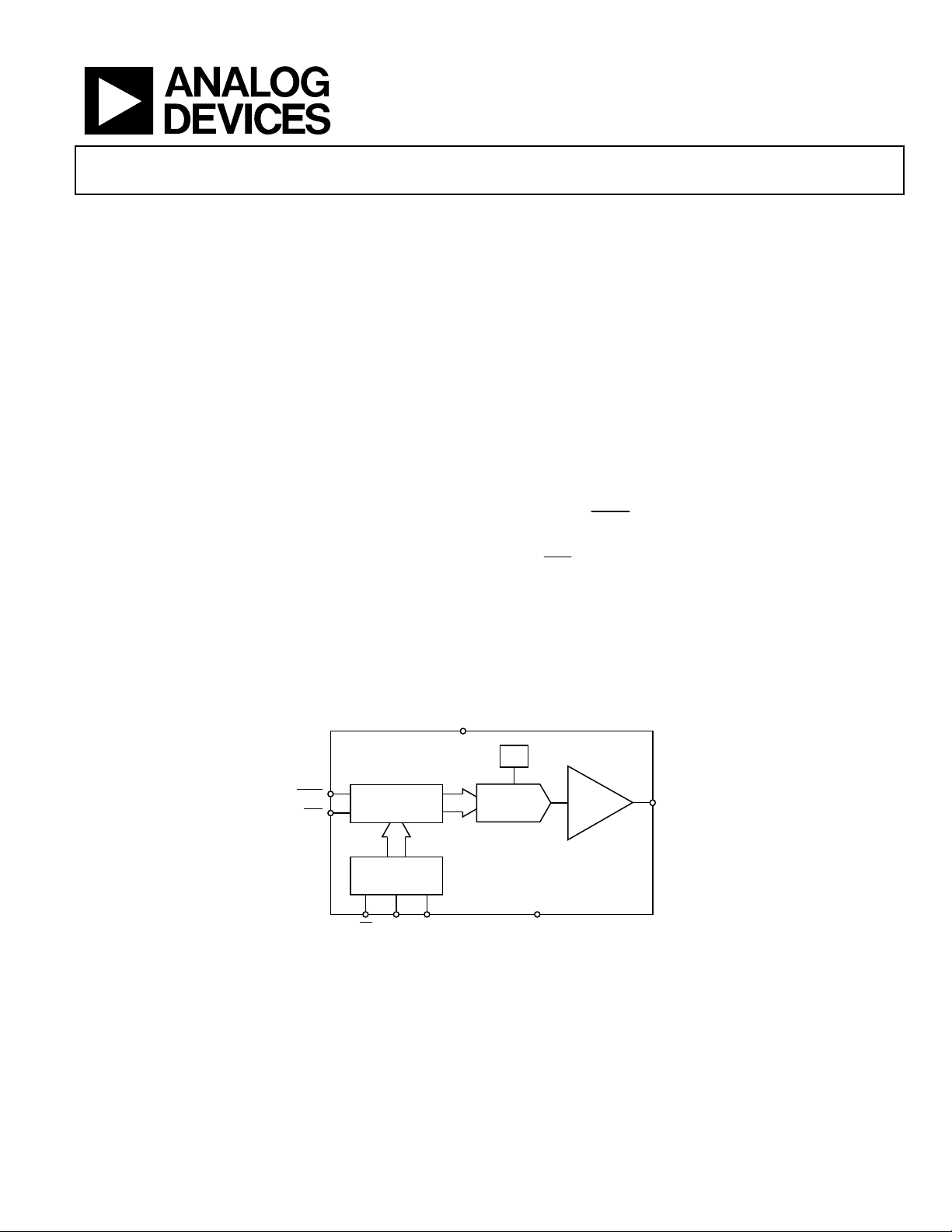
FUNCTIONAL BLOCK DIAGRAM
AD5626
LDAC
CLR
Rev. A
Information furnished by Analog Devices is believed to be accurate and reliable. However, no
responsibility is assumed by Analog Devices for its use, nor for any infringements of patents or other
rights of third parties that may result from its use. Specifications subject to change without notice. No
license is granted by implication or otherwise under any patent or patent rights of Analog Devices.
Trademarks and registered trademarks are the property of their respective owners.
DAC REGISTER
INPUT
REGIS TER
CS SCLK SDIN GND
DD
12-BIT DAC
Figure 1.
REF
OUTPUT
BUFFER
One Technology Way, P.O. Box 9106, Norwood, MA 02062-9106, U.S.A.
Tel: 781.329.4700 www.analog.com
Fax: 781.461.3113 ©2007—2009 Analog Devices, Inc. All rights reserved.
V
OU
06757-001
Page 2

AD5626
TABLE OF CONTENTS
Features .............................................................................................. 1
Applications ....................................................................................... 1
General Description ......................................................................... 1
Functional Block Diagram .............................................................. 1
Revision History ............................................................................... 2
Specifications ..................................................................................... 3
Electrical Characteristics ............................................................. 3
Timing Characteristics ................................................................ 4
Absolute Maximum Ratings ............................................................ 5
ESD Caution .................................................................................. 5
Pin Configurations and Function Descriptions ........................... 6
Typical Performance Characteristics ............................................. 7
Theory of Operation ...................................................................... 10
DAC Section ................................................................................ 10
Amplifier Section........................................................................ 10
Output Section ............................................................................ 10
Power Supply ............................................................................... 10
Timing and Control ................................................................... 11
Applications Information .............................................................. 12
Power Supplies, Bypassing, and Grounding ........................... 12
Unipolar Output Operation ...................................................... 12
Operating the AD5626 on 12 V or 15 V Supplies Only ........ 13
Measuring Offset Error ............................................................. 13
Bipolar Output Operation ......................................................... 13
Generating a Negative Supply Voltage .................................... 15
A Single-Supply, Programmable Current Source .................. 15
Galvanically-Isolated Interface ................................................. 15
Microprocessor Interfacing ....................................................... 16
Outline Dimensions ....................................................................... 17
Ordering Guide .......................................................................... 17
REVISION HISTORY
1/09—Rev. 0 to Rev. A
Change to Full-Scale Tempco Paramter and Full-Scale
Voltage (Min) Parameter ................................................................. 3
12/07—Revision 0: Initial Version
Rev. A | Page 2 of 20
Page 3

AD5626
SPECIFICATIONS
ELECTRICAL CHARACTERISTICS
@ VDD = 5.0 V ± 5%, −40°C ≤ TA ≤ +85°C, B grade device, unless otherwise noted.
Table 1.
Parameter Symbol Condition Min Typ Max Unit
STATIC PERFORMANCE
Resolution N 12 Bits
Relative Accuracy INL −1 ±1/4 +1 LSB
Differential Nonlinearity DNL No missing codes −1 ±3/4 +1 LSB
Zero-Scale Error V
Full-Scale Voltage VFS Data = 0xFFF1 4.079 4.095 4.111 V
Full-Scale Tempco
2, 3
TCVFS 20 ppm/°C
ANALOG OUTPUT
Output Current I
Load Regulation at Midscale L
Capacitive Load CL No oscillation2 500 pF
LOGIC INPUTS
Logic Input
Low Voltage VIL 0.8 V
High Voltage VIH 2.4 V
Input Leakage Current IIL 10 μA
Input Capacitance CIL 10 pF
AC CHARACTERISTICS2
Voltage Output Settling Time tS To ±1 LSB of final value3 16 μs
DAC Glitch 15 nV-s
Digital Feedthrough 15 nV-s
SUPPLY CHARACTERISTICS
Positive Supply Current IDD VIH = 2.4 V, VIL = 0.8 V, no load 1.5 2.5 mA
V
Power Dissipation P
V
Power Supply Sensitivity PSS ΔVDD = ±5% 0.002 0.004 %/%
1
Includes internal voltage reference error.
2
These parameters are guaranteed by design and not subject to production testing.
3
The settling time specification does not apply for negative going transitions within the last 6 LSBs of ground. Some devices exhibit double the typical settling time in
this 6 LSB region.
Data = 0x000 1/2 3 LSB
ZSE
Data = 0x800 ±5 ±7 mA
OUT
RL = 402 Ω to ∞, data = 0x800 1 3 LSB
REG
= 5 V, VIL = 0 V, no load 0.5 1 mA
DD
V
DISS
= 2.4 V, VIL = 0.8 V, no load 7.5 12.5 mW
IH
= 5 V, VIL = 0 V, no load 2.5 5 mW
DD
Rev. A | Page 3 of 20
Page 4
AD5626
V
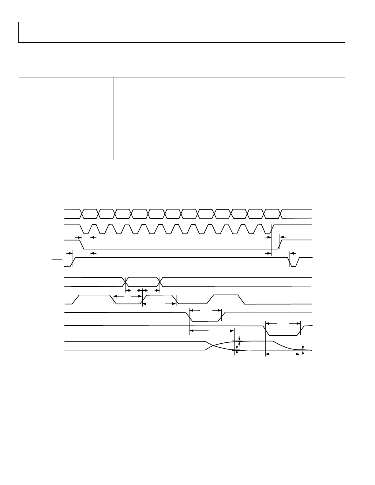
TIMING CHARACTERISTICS
@ VDD = 5.0 V ± 5%, −40°C ≤ TA ≤ +85°C, unless otherwise noted.
Table 2.
Parameter
tCH 30 ns min Clock width high
tCL 30 ns min Clock width low
t
LDW
tDS 15 ns min Data setup
t
15 ns min Data hold
DH
t
CLRW
t
15 ns min Load setup
LD1
t
10 ns min Load hold
LD2
t
30 ns min Select
CSS
t
CSH
1
These parameters are guaranteed by design and not subject to production testing.
2
All input control signals are specified with tr = tf = 5 ns (10% to 90% of 5 V) and timed from a voltage level of 1.6 V.
Timing Diagram
1, 2
Limit at T
MIN
, T
Unit Description
MAX
20 ns min Load pulse width
30 ns min Clear pulse width
20 ns min Deselect
OUT
SDIN
SCLK
CS
LDAC
SDIN
SCLK
LDAC
CLR
FS
ZS
D11 D10 D9 D8 D7 D6 D5 D4
t
CSS
t
LD1
t
t
DS
t
CL
DH
t
CH
Figure 2. Timing Diagram
t
D3 D2 D1 DO
LDW
t
S
±1 LSB
ERROR BAND
t
LD2
t
CLRW
t
CSH
t
S
06757-002
Rev. A | Page 4 of 20
Page 5
AD5626
ABSOLUTE MAXIMUM RATINGS
Table 3.
Parameter Rating
VDD to GND −0.3 V to +10 V
Logic Inputs to GND −0.3 V to VDD + 0.3 V
V
to GND −0.3 V to VDD + 0.3 V
OUT
I
Short Circuit to GND 50 mA
OUT
Package Power Dissipation (TJ max − TA)/θJA
Thermal Resistance (θJA)
8-Lead MSOP 220°C/W
8-Lead LFCSP 62°C/W
Maximum Junction Temperature
max)
(T
J
Operating Temperature Range −40°C to +85°C
Storage Temperature Range −65°C to +150°C
Lead Temperature JEDEC industry standard
Soldering J-STD-020
150°C
Stresses above those listed under Absolute Maximum Ratings
may cause permanent damage to the device. This is a stress
rating only; functional operation of the device at these or any
other conditions above those indicated in the operational
section of this specification is not implied. Exposure to absolute
maximum rating conditions for extended periods may affect
device reliability.
ESD CAUTION
Rev. A | Page 5 of 20
Page 6
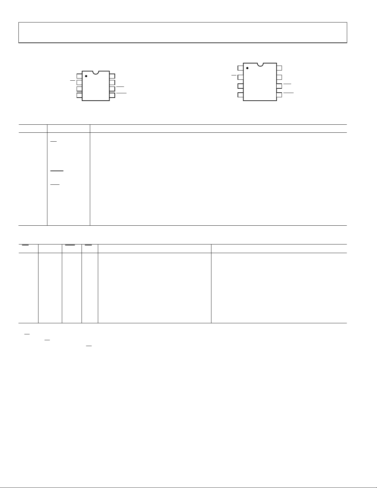
AD5626
PIN CONFIGURATIONS AND FUNCTION DESCRIPTIONS
V
CS
SCLK
SDIN
DD
1
AD5626
2
TOP VIEW
3
(Not to Scal e)
4
8
7
6
5
V
OUT
GND
CLR
LDAC
V
1
DD
2
3
(Not to Scale)
4
AD5626
TOP VIEW
CS
SCLK
6757-003
SDIN
8
7
6
5
V
OUT
GND
CLR
LDAC
6757-004
Figure 3. 8-Lead MSOP Pin Configuration Figure 4. 8-Lead LFCSP Pin Configuration
Table 4. Pin Function Descriptions
Pin No. Mnemonic Description
1 VDD Positive Supply. Nominal value 5 V ± 5%.
2
CS
Chip Select. Active low input.
3 SCLK Clock Input. Clock input for the internal serial input shift register.
4 SDIN
Serial Data Input. Data on this pin is clocked into the internal serial register on positive clock edges of the
SCLK pin. The most significant bit (MSB) is loaded first.
5
Serial Register Data Write to DAC Register. Active low input that writes the serial register data into the DAC
LDAC
register. Asynchronous input.
6
Clear DAC Register. Active low digital input that clears the DAC register to zero, setting the DAC to minimum
CLR
scale. Asynchronous input.
7 GND Ground. Analog ground for the DAC. This also serves as the digital logic ground reference voltage.
8 V
OUT
Voltage Output from the DAC. Fixed output voltage range of 0 V to 4.095 V with 1 mV/LSB. An internal
temperature stabilized reference maintains a fixed full-scale voltage independent of time, temperature, and
power supply variations.
Table 5. Control Logic Truth Table1
CS
2, 3
2
CLK
CLR
LD
4
Serial Shift Register Function DAC Register Function
H X H H No effect Latched
L L H H No effect Latched
L H H H No effect Latched
L
↑+
↑+
L H H Shift-register-data advanced one bit Latched
H X H
H H Shift-register-data advanced one bit Latched
No effect Updated with current shift register contents
↓–
H X H L No effect Transparent
H X L X No effect Loaded with all zeros
H X
1
↑+ indicates a positive logic transition; ↓– indicates a negative logic transition; X = don’t care.
2
CS and CLK are interchangeable.
3
Returning CS high avoids an additional false clock of serial data input.
4
Do not clock in serial data while LD is low.
↑+
H No effect Latched all zeros
Rev. A | Page 6 of 20
Page 7

AD5626
TYPICAL PERFORMANCE CHARACTERISTICS
5
4
3
2
OUTPUT VOLTAGE (V)
1
0
10 100k
RL TIED TO 5V
DATA = 0x000
100 1k 10k
LOAD RESIST ANCE ()
RL TIED TO AGND
DATA = 0xFFF
Figure 5. Output Voltage vs. Load
100
+85°C
+25°C
–40°C
10
1
0.1
0.01
0.001
OUTPUT PULL-DOWN VOLTAGE (mV)
0.0001
11
10 100
OUTPUT SI NK CURRENT (µA)
Figure 6. Output Pull-Down Voltage vs. Output Sink Current Capability
80
60
40
20
0
–20
OUTPUT CURRENT (mA)
–40
–60
1.002.04.03.01.50.5 2.5 4.53.5 5.0
OUTPUT VOLTAGE (V)
Figure 7. Short-Circuit Current
VDD = 5V
T
= 25°C
A
1
06757-005
CH1 5.00V CH2 100mV M2.00ms A CH1 210µV
Figure 8. Broadband Noise
1.2
1.1
1.0
0.9
0.8
0.7
0.6
0.5
SUPPLY CURRENT (mA)
0.4
0.3
06757-006
000
0.2
05
1.0 2.0 3.0 4.00.5 1.5 2.5 3.5 4.5
LOGIC VOLTAGE VALUE (V)
Figure 9. Supply Current vs. Logic Input Voltage
80
70
60
50
40
30
20
10
POWER SUPPL Y REJECTIO N (dB)
0
06757-007
–10
10 100k
100 1k 10k
FREQUENCY (Hz)
Figure 10. Power Supply Rejection vs. Frequency
06757-008
06757-009
.0
06757-010
Rev. A | Page 7 of 20
Page 8

AD5626
5.0
4.8
4.6
MIN (V)
DD
4.4
V
4.2
4.0
0.01 10
VFS 1 LSB
DATA = 0xFFF
T
= 25°C
A
PROPER OPERATION
WHEN V
VOLTAGE IS ABOVE
CURVE
SUPPLY
DD
0.1 1
OUTPUT LOAD CURRENT (mA)
Figure 11. Minimum Supply Voltage vs. Load
1
LDAC
2
OUTPUT
06757-011
SOURCE
CH1
CH2
VERTICLE SCALE
2.00V/DIV
200mV/DIV
OFFSET
–1.95V
3.9875mV
HORIZONT AL SCALE
5.0µs/DIV
5.0µs/DIV
POSITION
22.725µs
22.725µs
06757-014
Figure 14. Rise Time Detail
2.11
2.10
2.09
2.08
(V)
2.07
OUT
V
2.06
2.05
2.04
2.03
TIME (ns)
Figure 12. Midscale DAC Glitch Performance
0x7FF 0x800
0x800 0x7FF
1
LDAC
2
OUTPUT
06757-012
4.00 0.5 1.0 1.5 2.0 2.5 3.53.0
SOURCE
CH1
CH2
VERTICLE SCALE
2.00V/DIV
200mV/DIV
OFFSET
–1.95V
87.6mV
HORIZONT AL SCALE
5.0µs/DIV
5.0µs/DIV
POSITION
22.725µs
22.725µs
06757-015
Figure 15. Fall Time Detail
0.20
0.15
0.10
0.05
+85°C
+25°C
–40°C
SOURCE
CH2
VERTICLE SCALE
1.00V/DIV
OFFSET
2.90V
HORIZONT AL SCALE
50.0µs/DIV
Figure 13. Large Signal Settling Time
OUTPUT
POSITION
105.758µs
2
06757-013
Rev. A | Page 8 of 20
0
INL (LSB)
–0.05
–0.10
VDD = 5V
–0.15
0 4000
500 1000 1500 2000 2500 3000 3500
CODE
Figure 16. Integral Linearity Error vs. Digital Code
06757-016
Page 9

AD5626
60
50
40
30
20
NNUMBER OF UNITS
10
0
–12
–8 –4 0 4 8 12
TOTAL UNADJUST ED ERROR (mV)
TUE = INL + ZS + FS
SS = 300 UNITS
= 25°C
T
A
Figure 17. Total Unadjusted Error Histogram
4.115
4.110
4.105
AVG + 3
AVG
AVG – 3
–50 125
–25 0 25 50 75 100
FULL-SCALE OUTPUT (V)
4.100
4.095
4.090
4.085
4.080
4.075
VDD = 5V
NO LOAD
SS = 300 UNITS
TEMPERATURE ( °C)
Figure 18. Full-Scale Output Voltage vs. Temperature
0.50
0.45
0.40
0.35
0.30
0.25
0.20
ZERO SCALE ( mV)
0.15
0.10
0.05
0
–20 0 20 40 60 80
–40
TEMPERATURE ( °C)
06757-017
06757-018
06757-019
10
VDD = 5V
NO LOAD
DATA = 0xFFF
1
0.1
OUTPUT NOI SE DENSIT Y (µV/Hz)
0.01
10 100k
100 1k 10k
FREQUENCY (Hz)
06757-020
Figure 20. Output Voltage Noise vs. Frequency
5
4
3
2
1
0
–1
–2
–3
OUTPUT VO LTAGE CHANGE (mV)
READINGS NORMAL IZED
–4
TO ZERO HOUR TIME PO INT
–5
01
200 400 600 800 1000
HOURS OF OPERATION AT 125°C
AVERAGE
135 UNITS TES TED
RANGE
06757-021
200
Figure 21. Long-Term Drift Accelerated by Burn-In
1.6
1.4
1.2
1.0
0.8
0.6
SUPPLY CURRENT (mA)
0.4
0.2
0
–40
–200 20406080
TEMPERATURE ( °C)
VDD = 4.75V
V
= 5V
DD
V
= 5.25V
DD
06757-022
Figure 19. Zero-Scale Voltage vs. Temperature Figure 22. Supply Current vs. Temperature
Rev. A | Page 9 of 20
Page 10

AD5626
V
V
THEORY OF OPERATION
The AD5626 is a complete, ready-to-use, 12-bit digital-to-analog
converter (DAC). It contains a voltage-switched, 12-bit, lasertrimmed DAC, a curvature-corrected band gap reference, a
rail-to-rail output op amp, a DAC register, and a serial data
input register. The serial data interface consists of an SCLK,
serial data in (SDIN), and a load strobe (
3-wire interface offers maximum flexibility for interface to the
widest variety of serial data input loading requirements. In
addition, a
and a power-on-reset
CS
select is provided for multiple packaging loading
CLR
pin to simplify start or periodic resets.
DAC SECTION
The DAC is a 12-bit voltage mode device with an output that
swings from the GND potential to the 2.5 V internal band gap
voltage. It uses a laser trimmed, rail-to-rail ladder which is
switched by N-channel MOSFETs. The output voltage of the
DAC has a constant resistance independent of digital input
code. The DAC output internally connects to the rail-to-rail
output op amp.
AMPLIFIER SECTION
A low power consumption, precision amplifier buffers the DAC
output. This amplifier contains a differential PNP pair input
stage that provides low offset voltage and low noise, as well as
the ability to amplify the zero-scale DAC output voltages.
The rail-to-rail amplifier is configured with a gain of 1.6384
(= 4.095 V/2.5 V) to set the 4.095 V full-scale output (1 mV/LSB).
See Figure 23 for an equivalent circuit schematic of the analog
section.
OLTAGE SWITCHED 12-BI T
BAND GAP
REFERENCE
2.5V
Figure 23. Equivalent AD5626 Schematic of Analog Section
RAIL-TO -RAIL CONVERTER
BUFFER
N-CHANNEL FET
SPDT
SWITCHES
The op amp has a 16 μs typical settling time to 0.01%. There are
slight differences in settling time for negative slewing signals vs.
positive slewing signals. See the oscilloscope photos in the
Typical Performance Characteristics section of this data sheet.
OUTPUT SECTION
The rail-to-rail output stage of this amplifier is designed to
provide precision performance when operating near either
power supply.
LDAC
2R
R
2R
R
2R
2R
2R
). This basic
RAIL-TO- RAIL
OUTPUT
AMPLIFIER
R2
R1
A
= 1.638
V
(= 4.095V/ 2.5V)
V
OUT
06757-023
Rev. A | Page 10 of 20
DD
P-CH
V
OUT
N-CH
AGND
06757-024
Figure 24. Equivalent Analog Output Circuit
Figure 24 shows an equivalent output schematic of the rail-torail amplifier with its N-channel pull-down FETs that pull an
output load directly to GND. The output sourcing current is
provided by a P-channel pull-up device that can supply GND
terminated loads, especially at the low supply tolerance values
of 4.75 V. Figure 5 and Figure 6 provide information on output
swing performance near ground and full-scale as a function of
load. In addition to resistive load driving capability, the amplifier
has also been carefully designed and characterized for up to
500 pF capacitive load driving capability.
POWER SUPPLY
The very low power consumption of the AD5626 is a direct
result of a circuit design optimizing use of the CBCMOS process.
By using the low power characteristics of the CMOS for the
logic, and the low noise, tight matching of the complementary
bipolar transistors, good analog accuracy is achieved.
For power consumption sensitive applications, it is important
to note that the internal power consumption of the AD5626
is strongly dependent on the actual logic input voltage levels
CS
present on the SDIN,
LDAC
,
inputs are standard CMOS logic structures, they contribute
static power dissipation dependent on the actual driving
Logic V
and Logic VOL voltage levels. The graph in
OH
shows the effect on total AD5626 supply current as a function
of the actual value of input logic voltage. Consequently, use of
CMOS logic vs. TTL minimizes power dissipation in the static
state. A V
= 0 V on the SDIN,
IL
lowest standby power dissipation of 2.5 mW (500 μA × 5 V).
As with any analog system, it is recommended that the AD5626
power supply be bypassed on the same PC card that contains
the chip. Figure 10 shows the power supply rejection vs. frequency
performance. This should be taken into account when using higher
frequency, switched mode power supplies with ripple frequencies
of 100 kHz and higher.
One advantage of the rail-to-rail output amplifier used in the
AD5626 is the wide range of usable supply voltage. The part is
fully specified and tested over temperature for operation from
4.75 V to 5.25 V. If reduced linearity and source current capability near full scale can be tolerated, operation of the AD5626
is possible down to 4.3 V. The minimum operating supply
, and
CS
CLR
pins. Because these
CLR
, and
pins provides the
Figure 9
Page 11

AD5626
voltage vs. load current plot, shown in Figure 11, provides
information for operation below V
= 4.75 V.
DD
TIMING AND CONTROL
The AD5626 has a separate serial input register from the
12-bit DAC register that allows preloading of a new data value
into the serial register without disturbing the present DAC
output voltage. After the new value is fully loaded in the serial
input register, it can be asynchronously transferred to the DAC
register by strobing the
level sensitive
any new data is loaded into the serial input register. At any time,
the contents of the DAC register can be reset to zero by strobing
CLR
the
volts. details all of the timing requirements together
Figure 2
with , the control logic truth table.
Table 5
LDAC
pin that causes the DAC output voltage to go to zero
LDAC
pin. The DAC register uses a
strobe that should be returned high before
Rev. A | Page 11 of 20
Page 12

AD5626
V
V
APPLICATIONS INFORMATION
POWER SUPPLIES, BYPASSING, AND GROUNDING
All precision converter products require careful application of
good grounding practices to maintain full rated performance.
Because the AD5626 has been designed for 5 V applications, it
is ideal for those applications under microprocessor or microcomputer control. In these applications, digital noise is prevalent;
therefore, special care must be taken to ensure that its inherent
precision is maintained by exercising particularly good engineering
judgment when addressing the power supply, grounding, and
bypassing issues using the AD5626.
Use a well-filtered and regulated power supply for the AD5626.
The device has been completely characterized for a 5 V supply
with a tolerance of ±5%. Because a 5 V logic supply is almost
universally available, it is not recommended to connect the
DAC directly to an unfiltered logic supply without careful
filtering. Tapping a logic circuit supply for the DAC supply
is unwise because fast logic with nanosecond transition edges
induce high current pulses. The high transient current pulses
can generate glitches hundreds of millivolts in amplitude due
to wiring resistances and inductances. This high frequency
noise corrupts the analog circuits internal to the DAC and
causes errors.
Even though their spike noise is lower in amplitude, directly
tapping the output of a 5 V system supply can cause errors
because these supplies are of the switching regulator type that
can and do generate a great deal of high frequency noise. Therefore, power the DAC and any associated analog circuitry directly
from the system power supply outputs using appropriate filtering.
Figure 25 illustrates how a clean, analog-grade supply can be
generated from a 5 V logic supply using a differential LC filter
with separate power supply and return lines. With the values
shown, this filter can easily handle 100 mA of load current
without saturating the ferrite cores. Higher current capacity
can be achieved with larger ferrite cores. For lowest noise, all
electrolytic capacitors should be of the low equivalent series
resistance (ESR) type.
5V
FERRITE BEADS:
2 TURNS
Analog Supply
+ +
100µF
ELECT.
10-20µF
TANT.
0.1µF
CER.
+5V
+5V
RETURN
06757-025
TTL/CMOS
LOGIC
CIRCUITS
POWER SUPPLY
Figure 25. Properly Filtering a 5 V Logic Supply Yields a High Quality
To fit the AD5626 in an 8-lead package, only one ground
connection to the device is accommodated. The ground
connection of the DAC serves as the return path for supply
currents as well as the reference point for the digital input
thresholds. The ground connection also serves as the supply rail
for the internal voltage reference and the output amplifier.
Therefore, to minimize errors, connect the ground connection
of the AD5626 to a high quality analog ground, such as the one
previously described. Generous bypassing of the DACs supply
effectively reduces supply line induced errors. Local supply
bypassing consisting of a 10 μF tantalum electrolytic capacitor
in parallel with a 0.1 μF ceramic capacitor is recommended.
Connect the decoupling capacitors between the DAC supply
pin (Pin 1) and the analog ground (Pin 7).
Figure 26 shows how the ground and bypass connections
should be made to the AD5626.
5
1
CS
CLR
LDAC
SCLK
SDIN
V
2
6
5
3
4
DD
AD5626
V
OUT
GND
7
TO ANALOG GROUND
+
10µF
8
0.1µF
V
OUT
06757-026
Figure 26. Recommended Grounding and Bypassing Scheme for the AD5626
UNIPOLAR OUTPUT OPERATION
This is the basic mode of operation for the AD5626. As shown
in Figure 27, the AD5626 is designed to drive loads as low as
2 kΩ in parallel with 500 pF. The code table for this operation is
provided in Ta b le 6 .
5
10µF
0.1µF
2
CS
CLR
LDAC
SCLK
SDIN
6
AD5626
5
3
4
Figure 27. Unipolar Output Operation
Table 6. Unipolar Code Table
Hexadecimal Number
in DAC Register
FFF 4095 4.095
801 2049 2.049
800 2048
7FF 2047
000 0 0
+
1
V
DD
8
V
OUT
GND
7
Decimal Number
in DAC Register
0V V
2k 500pF
Analog Output
Voltage (V)
2.048
2.047
OUT
4.095V
06757-027
Rev. A | Page 12 of 20
Page 13

AD5626
V
C
V
OPERATING THE AD5626 ON 12 V OR 15 V SUPPLIES ONLY
Although the AD5626 has been specified to operate on a single,
5 V supply, a single 5 V supply may not be available in many
applications. Because the AD5626 consumes no more than 2.5 mA
maximum, an integrated voltage reference, such as the ADR02,
can be used as the 5 V supply for the AD5626. See Figure 28 for
the circuit configuration. Notice that the output voltage of the
reference requires no trimming because of the excellent load
regulation and tight initial output voltage tolerance of the ADR02.
Although the maximum supply current of the AD5626 is 2.5 mA,
local bypassing of the ADR02 output with at least 0.1 μF at the
DAC voltage supply pin is recommended to prevent the internal
digital circuits of the DAC from affecting the internal voltage
reference of the DAC.
12V OR 15
ADR02
CS
CLR
LDAC
SCLK
SDIN
Figure 28. Operating the AD5626 on 12 V or 15 V Supplies Using an
1µF
2
6
4
2
6
5
3
4
1
V
DD
AD5626
GND
7
0.1µF
ADR02 Voltage Reference
8
V
OUT
06757-028
MEASURING OFFSET ERROR
One of the most commonly specified endpoint errors associated
with real world nonideal DACs is offset error. In most DAC
testing, the offset error is measured by applying the zero-scale
code and measuring the output deviation from 0 V.
There are some DACs where offset errors are present but not
observable at the zero scale because of other circuit limitations
(for example, zero coinciding with single-supply ground). In
these DACs, nonzero output at zero code cannot be read as the
offset error. In the AD5626, for example, the zero-scale error is
specified to be ±3 LSBs. Because zero scale coincides with zero
volt, it is not possible to measure negative offset error.
5
0.1µF
1
V
2
CS
CLR
LDA
SCLK
SDIN
SET CODE = 0x000 AND M EASURE V
6
5
3
4
DD
AD5626
GND
7
8
V
OUT
V–
OUT
V
OUT
200µA, MAXR
6757-029
Figure 29. Measuring Zero-Scale or Offset Error
By adding a pull-down resistor from the output of the AD5626
to a negative supply as shown in Figure 29, offset errors can be
read at zero code. This configuration forces the output P-channel
MOSFET to source current to the negative supply thereby allowing
the designer to determine in which direction the offset error
appears. The value of the resistor should be such that, at zero
code, current through the resistor is 200 μA, maximum.
BIPOLAR OUTPUT OPERATION
Although the AD5626 has been designed for single-supply
operation, bipolar operation is achievable using the circuit
illustrated in Figure 30. The circuit uses a single-supply, railto-rail OP295 op amp and the REF03 to generate the −2.5 V
reference required to level shift the DAC output voltage.
Note that the −2.5 V reference is generated without the use of
precision resistors. The circuit configuration provides an output
voltage in the range of −5 V ≤ V
mentary offset binary. Although each DAC LSB corresponds to
1 mV, each output LSB has been scaled to 2.44 mV. Ta bl e 7 lists
the relationship between the digital codes and output voltage.
The transfer function of the circuit is given by
O
and, for the circuit values shown, becomes
= −2.44 mV × Digital Code + 5 V
V
O
≤ +5 V and is coded in comple-
OUT
R4
CodeDigitalV
R1
R4
×+××−= 5.2mV1
R2
Rev. A | Page 13 of 20
Page 14

AD5626
V
V
V
2
CS
CLR
LDAC
SCLK
SDIN
6
5
3
4
0.1µF
10µF
+
+5V
ADR03
2
4
+5
1
V
DD
AD5626
GND
7
6
5
0.1µF
V
OUT
2.5V
TRIM
8
100
P1
10k
R1
10k
12.7k
–2.5V
R2
P2
10k
–
2
3
+
A1, A2 = 1/2 O P295
R3
247k
0.01µF
A1
FULL-SCALE
R4
23.7k
–
6
A2
5
+
ZERO-SCALE
ADJUST
1
ADJUST
+5V
8
4
–5V
500
–2.5V
P3
7
–5V V
+5
O
06757-030
Figure 30. Bipolar Output Operation
+5
0.1µF
2
ADR03
6
+2.5V
4
+5V
0.1µF
1
V
CS
CLR
LDAC
SCLK
SDIN
2
6
5
3
4
DD
AD5626
GND
7
V
OUT
Figure 31. Bipolar Output Operation Without Trim
Table 7. Bipolar Code
Hexadecimal Number
in DAC Register
Decimal Number
in DAC Register
Analog Output
Voltage (V)
FFF 4095 −4.9976
801 2049 −2.44E − 3
800 2048 0
7FF 2047 +2.44E − 3
000 0 +5
To maintain monotonicity and accuracy, R1, R2, and R4 should
be selected to match within 0.01% and must all be of the same
(preferably metal foil) type to assure temperature coefficient
R1
OUT
8
RANGE
±2.5V
±5V
R2
+5V
8
–
2
A1
3
+
4
R3
10k
10k 43.2k + 499
R4
R1
–5V
A1 = 1/2 OP295
R2
3
R
1
0
k
10k
1
0
20k
k
1
15k + 274
V
O
R4V
06757-031
matching. Mismatching between R1 and R2 causes offset and
gain errors whereas an R4 to R1 or R4 to R2 mismatch yields
gain errors.
For applications that do not require high accuracy, the circuit
illustrated in Figure 31 can also be used to generate a bipolar
output voltage. In this circuit, only one op amp is used and no
potentiometers are used for offset and gain trim. The output
voltage is coded in offset binary and is given by
R4
⎛
××= 5.21mV1
CodeDigitalV
O
⎜
+
R4R3
⎝
R2
⎞
⎛
+×
⎟
⎜
R1
⎠
⎝
⎞
⎟
⎠
R2
×−
R1
Rev. A | Page 14 of 20
Page 15

AD5626
W
V
A
For the ±2.5 V output range and the circuit values shown in the
table in Figure 31, the transfer equation becomes
V
= 1.22 mV × Digital Code − 2.5 V
O
Similarly, for the 5 V output range, the transfer equation
becomes
V
= 2.44 mV × Digital Code − 5 V
O
GENERATING A NEGATIVE SUPPLY VOLTAGE
Some applications may require bipolar output configuration
but only have a single power supply rail available. This is very
common in data acquisition systems using microprocessorbased systems. In these systems, only 12 V, 15 V, and/or 5 V
are available.
Figure 32 shows a method for generating a negative supply
voltage using one CD4049, a CMOS hexadecimal inverter, and
operating on 12 V or 15 V. The circuit is essentially a charge
pump where two of the six inverters are used as an oscillator.
For the values shown, the frequency of oscillation is approximately 3.5 kHz and is fairly insensitive to supply voltage
because R1 > 2 × R2.
The remaining four inverters are wired in parallel for higher
output current. The square wave output is level translated by C2
to a negative-going signal rectified using a pair of 1N4001s, and
then filtered by C3. With the values shown, the charge pump
provides an output voltage of −5 V for currents loading in the
range 0.5 mA ≤ I
I
≤ 7 mA with a 12 V supply.
OUT
INVERTERS = CD4049
5432
R1
510k
R2
5.1k
0.02µF
Figure 32. Generating a –5 V Supply When Only 12 V or 15 V Is Available
≤ 10 mA with a 15 V supply and 0.5 mA ≤
OUT
7
6
9
10
47µF
11
C1
14
+
12
15
D2
C2
1N4001
D1
+
1N4001
470
C3
47µF
R3
–5V
1N5231
5.1V
ZENER
A SINGLE-SUPPLY, PROGRAMMABLE CURRENT SOURCE
The circuit in Figure 33 shows how the AD5626 can be used
with an OP295 single-supply, rail-to-rail, output op amp to
provide a digitally programmable current sink from V
that consumes less than 3.8 mA, maximum. The DAC output
voltage is applied across R1 by placing the 2N2222 transistor in
the feedback loop of the OP295. For the circuit values shown,
the full-scale output current is 1 mA, which is given by the
following equation:
I
OUT
D
=
R1
V095.4×
where DW = the binary digital input code of the AD5626.
SOURCE
5
0.1µF
V
S
LOAD
1
2N2222
R1
4.02k
P1
200
FULL-SCALE
ADJUST
06757-033
CLR
LDAC
SCLK
SDIN
1
V
2
CS
6
5
3
4
DD
AD5626
GND
7
V
OUT
3
8
2
A1 = 1/2 OP295
+5V
+
A1
–
Figure 33. A Single-Supply, Programmable Current Source
The usable output voltage range of the current sink is 5 V to
60 V. The low limit of the range is controlled by transistor
saturation, and the high limit is controlled by the collector-base
breakdown voltage of the 2N2222.
GALVANICALLY-ISOLATED INTERFACE
In many process control type applications, it is necessary to
provide an isolation barrier between the controller and the unit
being controlled to protect and isolate the controlling circuitry
from any hazardous common-mode voltages that may occur.
An iCoupler® can provide isolation in excess of 2.5 kV. The
serial loading structure of the AD5626 makes it ideal for
isolated interfaces as the number of interface lines is kept to
a minimum. Figure 34 illustrates a 4-channel isolated interface
using an ADuM1400. For further information, visit
http://www.analog.com/icouplers.
MICROCONTROLLER
V
SERIAL CLOCK OUT
06757-032
SERIAL DATA OUT
SYNC OUT
CONTRO L OUT
*ADDITIONAL PINS OMI TTED FO R CLARITY.
IA
V
IB
V
IC
V
ID
Figure 34. An iCoupler-Isolated DAC Interface
DuM1400*
ENCODE DECODE
ENCODE DECODE
ENCODE DECODE
ENCODE DECODE
V
OA
TO SCLK
V
OB
TO SDIN
V
OC
TO SYNC
V
OD
TO LDAC
06757-034
Rev. A | Page 15 of 20
Page 16

AD5626
*
MICROPROCESSOR INTERFACING
AD5626 to MC68HC11 Interface
The circuit illustrated in Figure 35 shows a serial interface
between the AD5626 and the MC68HC11 8-bit microcontroller.
SCK of the MC68HC11 drives SCLK of the AD5626, whereas
the MOSI output drives the serial data line, SDIN, of the AD5626.
CLR
The
the PC1, PD5, and PC0 port lines, respectively, as shown.
For correct operation of the serial interface, configure the
MC68HC11 such that its CPOL bit is set to 1 and its CPHA bit
is also set to 1. When the serial data is to be transmitted to the
DAC, PC0 is taken low, asserting the
the MC68HC11 is configured in this manner, serial data on
MOSI is valid on the rising edge of SCLK. The MC68HC11
transmits its serial data in 8-bit bytes (MSB first), with only
eight rising clock edges occurring in the transmit cycle. To load
data to the input serial register of the AD5626, PC0 is left low
after the first eight bits are transferred, and a second byte of
LDAC
,
, and CS signals of the DAC are derived from
CS
input of the DAC. When
data is then transferred serially to the AD5626. During the
second byte load, the first 4 MSBs of the first byte are pushed
out of the input shift register of the DAC. At the end of the
second byte load, PC0 is taken high. To prevent accidental
advancing of the internal shift register, SCLK must already be
asserted before PC0 is taken high. To transfer the contents of
the input shift register to the DAC register, PD5 is taken low,
asserting the
LDAC
input. The
CLR
input of the DAC, controlled
by the MC68HC11 PC1 port, provides an asynchronous clear
function, setting the DAC output to zero.
MC68HC11*
PC1
PC0
PD5
SCK
MOSI
ADDITIONAL PINS OMI TTED FO R CLARITY.
Figure 35. AD5626 to MC68HC11 Interface
AD5626
CLR
CS
LDAC
SCLK
SDIN
06757-035
Rev. A | Page 16 of 20
Page 17

AD5626
OUTLINE DIMENSIONS
3.20
3.00
2.80
8
5
3.20
3.00
1
2.80
PIN 1
0.65 BSC
0.95
0.85
0.75
0.15
0.38
0.00
0.22
COPLANARITY
0.10
COMPLIANT TO JEDEC STANDARDS MO-187-AA
Figure 36. 8-Lead Mini Small Outline Package [MSOP]
3.00
BSC SQ
5.15
4.90
4.65
4
1.10 MAX
8°
0°
SEATING
PLANE
0.23
0.08
(RM-8)
Dimensions shown in millimeters
0.30
0.23
0.18
0.80
0.60
0.40
0.65 BSC
PIN 1 INDEX
AREA
0.80
0.75
0.70
SEATING
PLANE
TOP VIEW
0.80 MAX
0.55 NOM
0.50
0.40
0.30
0.05 MAX
0.02 NOM
0.20 REF
5
EXPOSED
(BOTTOM VIEW)
4
PAD
2.48
2.38
2.23
8
1.74
1.64
1.49
1
P
N
I
1
R
A
O
T
N
I
D
C
I
)
9
1
.
R
0
(
062507-A
Figure 37. 8-Lead Lead Frame Chip Scale Package [LFCSP_WD]
3 mm x 3 mm Body, Very Very Thin, Dual Lead
(CP-8-3)
Dimensions shown in millimeters
ORDERING GUIDE
Model INL (LSB) Temperature Range Package Description Package Option Branding
AD5626BRMZ
AD5626BRMZ-REEL71 ±1 –40°C to +85°C 8-Lead MSOP RM-8 DAP
AD5626BCPZ-REEL7
1
Z = RoHS Compliant Part.
1
1
±1 –40°C to +85°C 8-Lead LFCSP_WD CP-8-3 DAP
±1 –40°C to +85°C 8-Lead MSOP RM-8 DAP
Rev. A | Page 17 of 20
Page 18

AD5626
NOTES
Rev. A | Page 18 of 20
Page 19

AD5626
NOTES
Rev. A | Page 19 of 20
Page 20

AD5626
NOTES
©2007—2009 Analog Devices, Inc. All rights reserved. Trademarks and
registered trademarks are the property of their respective owners.
D06757-0-1/09(A)
Rev. A | Page 20 of 20
 Loading...