

Page 1
Quad, 12-/14-/16-Bit nanoDACs with
VDDV
/
S
FEATURES
Low power, smallest pin-compatible, quad nanoDACs
AD5664R: 16 bits
AD5644R: 14 bits
AD5624R: 12 bits
User-selectable external or internal reference
External reference default
On-chip 1.25 V/2.5 V, 5 ppm/°C reference
10-lead MSOP and 3 mm × 3 mm LFCSP_WD
2.7 V to 5.5 V power supply
Guaranteed monotonic by design
Power-on reset to zero scale
Per channel power-down
Serial interface, up to 50 MHz
APPLICATIONS
Process controls
Data acquisition systems
Portable battery-powered instruments
Digital gain and offset adjustment
Programmable voltage and current sources
Programmable attenuators
5 ppm/°C On-Chip Reference
AD5624R/AD5644R/AD5664R
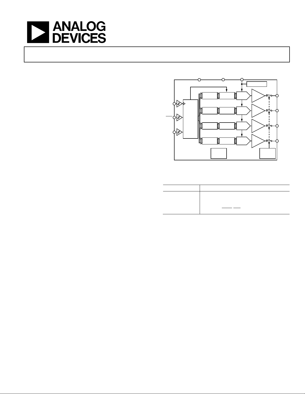
FUNCTIONAL BLOCK DIAGRAM
GND
AD5624R/AD5644R/AD5664R
INPUT
INPUT
INPUT
INPUT
REGISTER
REGISTER
REGISTER
REGISTER
POWER-ON
LOGIC
Figure 1.
REGISTER
SCLK
REGISTER
REGISTER
REGISTER
YNC
DIN
INTERFACE
LOGIC
Table 1. Related Devices
Part No. Description
AD5624/AD5664
2.7 V to 5.5 V quad, 12-/16-bit DACs, external
reference
AD5666
2.7 V to 5.5 V quad, 16-bit DAC, internal
reference, LDAC
DAC
DAC
DAC
DAC
V
REFIN
REFOUT
STRING
DAC A
STRING
DAC B
STRING
DAC C
STRING
DAC D
, CLR pins
1.25V/2.5V REF
BUFFER
BUFFER
BUFFER
BUFFER
POWER-
DOWN
LOGIC
V
A
OUT
V
B
OUT
V
C
OUT
V
D
OUT
5856-001
GENERAL DESCRIPTION
The AD5624R/AD5644R/AD5664R, members of the nanoDAC®
family, are low power, quad, 12-/14-/16-bit buffered voltage-out
DACs. All devices operate from a single 2.7 V to 5.5 V supply
and are guaranteed monotonic by design.
The AD5624R/AD5644R/AD5664R have an on-chip reference.
The AD56x4R-3 has a 1.25 V, 5 ppm/°C reference, giving a fullscale output range of 2.5 V; the AD56x4R-5 has a 2.5 V, 5 ppm/°C
reference giving a full-scale output range of 5 V. The on-chip
reference is off at power-up, allowing the use of an external reference; all devices can be operated from a single 2.7 V to 5.5 V
supply. The internal reference is enabled via a software write.
The part incorporates a power-on reset circuit that ensures the
DAC output powers up to 0 V and remains there until a valid
write takes place. The part contains a per-channel power-down
feature that reduces the current consumption of the device to
480 nA at 5 V and provides software-selectable output loads
while in power-down mode. The low power consumption of
Rev. B
Information furnished by Analog Devices is believed to be accurate and reliable. However, no
responsibility is assumed by Analog Devices for its use, nor for any infringements of patents or other
rights of third parties that may result from its use. Specifications subject to change without notice. No
license is granted by implication or otherwise under any patent or patent rights of Analog Devices.
Trademarks and registered trademarks are the property of their respective owners.
this part in normal operation makes it ideally suited to portable
battery-operated equipment.
The AD5624R/AD5644R/AD5664R use a versatile 3-wire serial
interface that operates at clock rates up to 50 MHz, and is compatible with standard SPI, QSPI™, MICROWIRE™, and DSP
interface standards. The on-chip precision output amplifier
enables rail-to-rail output swing.
PRODUCT HIGHLIGHTS
1. Quad 12-/14-/16-bit DACs.
2. On-chip 1.25 V/2.5 V, 5 ppm/°C reference.
3. Available in 10-lead MSOP and 10-lead, 3 mm × 3 mm,
LFCSP_WD.
4. Low power, typically consumes 1.32 mW at 3 V and
2.25 mW at 5 V.
One Technology Way, P.O. Box 9106, Norwood, MA 02062-9106, U.S.A.
Tel: 781.329.4700 www.analog.com
Fax: 781.461.3113 ©2006–2008 Analog Devices, Inc. All rights reserved.
Page 2

AD5624R/AD5644R/AD5664R
TABLE OF CONTENTS
Features .............................................................................................. 1
Applications ....................................................................................... 1
Functional Block Diagram .............................................................. 1
General Description ......................................................................... 1
Product Highlights ........................................................................... 1
Revision History ............................................................................... 2
Specifications ..................................................................................... 3
AD5624R-5/AD5644R-5/AD5664R-5 ....................................... 3
AD5624R-3/AD5644R-3/AD5664R-3 ....................................... 4
AC Characteristics ........................................................................ 6
Timing Characteristics ................................................................ 7
Timing Diagram ........................................................................... 7
Absolute Maximum Ratings ............................................................ 8
ESD Caution .................................................................................. 8
Pin Configuration and Function Descriptions ............................. 9
Typical Performance Characteristics ........................................... 10
Terminology .................................................................................... 18
Theory of Operation ...................................................................... 20
Digital-to-Analog Section ......................................................... 20
Resistor String ............................................................................. 20
Output Amplifier ........................................................................ 20
Internal Reference ...................................................................... 20
External Reference ..................................................................... 20
Serial Interface ............................................................................ 20
Input Shift Register .................................................................... 21
SYNC
Interrupt ........................................................................... 21
Power-On Reset .......................................................................... 22
Software Reset ............................................................................. 22
Power-Down Modes .................................................................. 22
LDAC Function ........................................................................... 23
Internal Reference Setup ........................................................... 23
Microprocessor Interfacing ....................................................... 24
Applications ..................................................................................... 25
Using a Reference as a Power Supply for the
AD5624R/AD5644R/AD5664R ............................................... 25
Bipolar Operation Using the
AD5624R/AD5644R/AD5664R ............................................... 25
Using AD5624R/AD5644R/AD5664R with a Galvanically
Isolated Interface ........................................................................ 25
Power Supply Bypassing and Grounding ................................ 26
Outline Dimensions ....................................................................... 27
Ordering Guide .......................................................................... 28
REVISION HISTORY
4/08—Rev. A to Rev. B
Changes to Figure 50 ...................................................................... 20
Updated Outline Dimensions ....................................................... 27
Changes to Ordering Guide .......................................................... 28
11/06—Rev. 0 to Rev. A
Changes to Reference Output Parameter in Table 2 .................... 3
Changes to Reference Output Parameter in Table 3 .................... 5
Added Note to Figure 3 .................................................................... 9
4/06—Revision 0: Initial Version
Rev. B | Page 2 of 28
Page 3

AD5624R/AD5644R/AD5664R
SPECIFICATIONS
AD5624R-5/AD5644R-5/AD5664R-5
VDD = 4.5 V to 5.5 V; RL = 2 kΩ to GND; CL = 200 pF to GND; V
= VDD; all specifications T
REFIN
MIN
to T
, unless otherwise noted.
MAX
Table 2.
B Grade
1
Parameter Min Typ Max Unit Conditions/Comments
STATIC PERFORMANCE
2
AD5664R
Resolution 16 Bits
Relative Accuracy ±8 ±16 LSB
Differential Nonlinearity ±1 LSB Guaranteed monotonic by design
AD5644R
Resolution 14 Bits
Relative Accuracy ±2 ±4 LSB
Differential Nonlinearity ±0.5 LSB Guaranteed monotonic by design
AD5624R
Resolution 12 Bits
Relative Accuracy ±0.5 ±1 LSB
Differential Nonlinearity ±0.25 LSB Guaranteed monotonic by design
Zero-Code Error 2 10 mV All zeroes loaded to DAC register
Offset Error ±1 ±10 mV
Full-Scale Error −0.1 ±1 % of FSR All ones loaded to DAC register
Gain Error ±1.5 % of FSR
Zero-Code Error Drift ±2 μV/°C
Gain Temperature Coefficient ±2.5 ppm Of FSR/°C
DC Power Supply Rejection Ratio −100 dB DAC code = midscale; VDD = 5 V ± 10%
DC Crosstalk
External Reference 10 μV Due to full-scale output change, RL = 2 kΩ to GND or V
10 μV/mA Due to load current change
5 μV Due to powering down (per channel)
Internal Reference 25 μV Due to full-scale output change, RL = 2 kΩ to GND or V
20 μV/mA Due to load current change
10 μV Due to powering down (per channel)
OUTPUT CHARACTERISTICS
3
Output Voltage Range 0 VDD V
Capacitive Load Stability 2 nF RL = ∞
10 nF RL = 2 kΩ
DC Output Impedance 0.5 Ω
Short-Circuit Current 30 mA VDD = 5 V
Power-Up Time 4 μs Coming out of power-down mode; VDD = 5 V
REFERENCE INPUTS
Reference Current 170 200 μA V
= VDD = 5.5 V
REF
Reference Input Range 0.75 VDD V
Reference Input Impedance 26 kΩ
REFERENCE OUTPUT
Output Voltage 2.495 2.505 V At ambient
Reference TC
3
±5 ±10 ppm/°C MSOP package models
±10 ppm/°C LFCSP package models
Output Impedance 7.5 kΩ
DD
DD
Rev. B | Page 3 of 28
Page 4

AD5624R/AD5644R/AD5664R
B Grade
1
Parameter Min Typ Max Unit Conditions/Comments
LOGIC INPUTS
3
Input Current ±2 μA All digital inputs
V
, Input Low Voltage 0.8 V VDD = 5 V
INL
V
, Input High Voltage 2 V VDD = 5 V
INH
Pin Capacitance 3 pF
POWER REQUIREMENTS
VDD 4.5 5.5 V
IDD VIH = VDD, VIL = GND, VDD = 4.5 V to 5.5 V
Normal Mode
4
0.45 0.9 mA Internal reference off
0.95 1.2 mA Internal reference on
All Power-Down Modes
1
Temperature range: B grade: −40°C to +105°C.
2
Linearity calculated using a reduced code range: AD5664R (Code 512 to Code 65,024); AD5644R (Code 128 to Code 16,256); AD5624R (Code 32 to Code 4064). Output
unloaded.
3
Guaranteed by design and characterization, not production tested.
4
Interface inactive. All DACs active. DAC outputs unloaded.
5
All DACs powered down.
5
0.48 1 μA
AD5624R-3/AD5644R-3/AD5664R-3
VDD = 2.7 V to 3.6 V; RL = 2 kΩ to GND; CL = 200 pF to GND; V
Table 3.
B Grade
1
Parameter Min Typ Max Unit Conditions/Comments
STATIC PERFORMANCE
2
AD5664R
Resolution 16 Bits
Relative Accuracy ±8 ±16 LSB
Differential Nonlinearity ±1 LSB Guaranteed monotonic by design
AD5644R
Resolution 14 Bits
Relative Accuracy ±2 ±4 LSB
Differential Nonlinearity ±0.5 LSB Guaranteed monotonic by design
AD5624R
Resolution 12 Bits
Relative Accuracy ±0.5 ±1 LSB
Differential Nonlinearity ±0.25 LSB Guaranteed monotonic by design
Zero-Code Error 2 10 mV All zeroes loaded to DAC register
Offset Error ±1 ±10 mV
Full-Scale Error −0.1 ±1 % of FSR All ones loaded to DAC register
Gain Error ±1.5 % of FSR
Zero-Code Error Drift ±2 μV/°C
Gain Temperature Coefficient ±2.5 ppm Of FSR/°C
DC Power Supply Rejection Ratio −100 dB DAC code = midscale; VDD = 3 V ± 10%
DC Crosstalk
External Reference 10 μV Due to full-scale output change, RL = 2 kΩ to GND or V
10 μV/mA Due to load current change
5 μV Due to powering down (per channel)
Internal Reference 25 μV Due to full-scale output change, RL = 2 kΩ to GND or V
20 μV/mA Due to load current change
10 μV Due to powering down (per channel)
= VDD; all specifications T
REFIN
MIN
to T
, unless otherwise noted.
MAX
DD
DD
Rev. B | Page 4 of 28
Page 5

AD5624R/AD5644R/AD5664R
B Grade
1
Parameter Min Typ Max Unit Conditions/Comments
OUTPUT CHARACTERISTICS
3
Output Voltage Range 0 VDD V
Capacitive Load Stability 2 nF RL = ∞
10 nF RL = 2 kΩ
DC Output Impedance 0.5 Ω
Short-Circuit Current 30 mA VDD = 3 V
Power-Up Time 4 μs Coming out of power-down mode; VDD = 3 V
REFERENCE INPUTS
Reference Current 170 200 μA V
= VDD = 3.6 V
REF
Reference Input Range 0 VDD V
Reference Input Impedance 26 kΩ
REFERENCE OUTPUT
Output Voltage 1.247 1.253 V At ambient
Reference TC
3
±5 ±15 ppm/°C MSOP package models
±10 ppm/°C LFCSP package models
Output Impedance 7.5 kΩ
LOGIC INPUTS
3
Input Current ±2 μA All digital inputs
V
, Input Low Voltage 0.8 V VDD = 3 V
INL
V
, Input High Voltage 2 V VDD = 3 V
INH
Pin Capacitance 3 pF
POWER REQUIREMENTS
VDD 2.7 3.6 V
IDD VIH = VDD, VIL = GND, VDD = 2.7 V to 3.6 V
Normal Mode
4
0.44 0.85 mA Internal reference off
0.95 1.15 mA Internal reference on
All Power-Down Modes
1
Temperature range: B grade: −40°C to +105°C.
2
Linearity calculated using a reduced code range: AD5664R (Code 512 to Code 65,024); AD5644R (Code 128 to Code 16,256); AD5624R (Code 32 to Code 4064). Output
unloaded.
3
Guaranteed by design and characterization, not production tested.
4
Interface inactive. All DACs active. DAC outputs unloaded.
5
All DACs powered down.
5
0.2 1 μA
Rev. B | Page 5 of 28
Page 6

AD5624R/AD5644R/AD5664R
AC CHARACTERISTICS
VDD = 2.7 V to 5.5 V; RL = 2 kΩ to GND; CL = 200 pF to GND; V
= VDD; all specifications T
REFIN
MIN
to T
, unless otherwise noted.1
MAX
Table 4.
Parameter
2
Min Typ Max Unit Conditions/Comments
3
Output Voltage Settling Time
AD5624R 3 4.5 μs ¼ to ¾ scale settling to ±0.5 LSB
AD5644R 3.5 5 μs ¼ to ¾ scale settling to ±0.5 LSB
AD5664R 4 7 μs ¼ to ¾ scale settling to ±2 LSB
Slew Rate 1.8 V/μs
Digital-to-Analog Glitch Impulse 10 nV-s 1 LSB change around major carry
Digital Feedthrough 0.1 nV-s
Reference Feedthrough −90 dB V
= 2 V ± 0.1 V p-p, frequency 10 Hz to 20 MHz
REF
Digital Crosstalk 0.1 nV-s
Analog Crosstalk 1 nV-s External reference
4 nV-s Internal reference
DAC-to-DAC Crosstalk 1 nV-s External reference
4 nV-s Internal reference
Multiplying Bandwidth 340 kHz V
Total Harmonic Distortion −80 dB V
= 2 V ± 0.1 V p-p
REF
= 2 V ± 0.1 V p-p, frequency = 10 kHz
REF
Output Noise Spectral Density 120 nV/√Hz DAC code = midscale, 1 kHz
100 nV/√Hz DAC code = midscale, 10 kHz
Output Noise 15 μV p-p 0.1 Hz to 10 Hz
1
Guaranteed by design and characterization, not production tested.
2
See the Terminology section.
3
Temperature range is −40°C to +105°C, typical at 25°C.
Rev. B | Page 6 of 28
Page 7
AD5624R/AD5644R/AD5664R
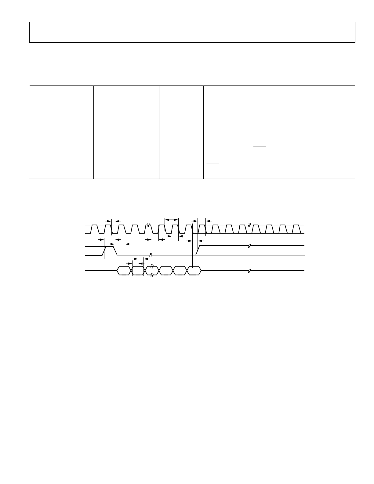
TIMING CHARACTERISTICS
All input signals are specified with tR = tF = 1 ns/V (10% to 90% of VDD) and timed from a voltage level of (VIL + VIH)/2 (see Figure 2).
V
= 2.7 V to 5.5 V; all specifications T
DD
Table 5.
Limit at T
Parameter VDD = 2.7 V to 5.5 V Unit Conditions/Comments
2
t
1
20 ns min SCLK cycle time
t2 9 ns min SCLK high time
t3 9 ns min SCLK low time
t4 13 ns min
t5 5 ns min Data setup time
t6 5 ns min Data hold time
t7 0 ns min
t8 15 ns min
t9 13 ns min
t10 0 ns min
1
Guaranteed by design and characterization, not production tested.
2
Maximum SCLK frequency is 50 MHz at VDD = 2.7 V to 5.5 V.
TIMING DIAGRAM
t
10
SCLK
t
8
SYNC
DIN
MIN
t
to T
MIN
, T
MAX
4
, unless otherwise noted.1
MAX
t
1
t
t
3
t
6
t
5
2
DB0DB23
Figure 2. Serial Write Operation
to SCLK falling edge setup time
SYNC
SCLK falling edge to SYNC
Minimum SYNC
rising edge to SCLK fall ignore
SYNC
SCLK falling edge to SYNC
t
9
t
7
high time
rising edge
fall ignore
05856-002
Rev. B | Page 7 of 28
Page 8
AD5624R/AD5644R/AD5664R
ABSOLUTE MAXIMUM RATINGS
TA = 25°C, unless otherwise noted.
Table 6.
Parameter Rating
VDD to GND −0.3 V to +7 V
V
to GND −0.3 V to VDD + 0.3 V
OUT
V
REFIN/VREFOUT
Digital Input Voltage to GND −0.3 V to VDD + 0.3 V
Operating Temperature Range
Industrial −40°C to +105°C
Storage Temperature Range −65°C to +150°C
Junction Temperature (TJ max) 150°C
Power Dissipation (TJ max − TA)/θJA
Thermal Impedance
LFCSP_WD Package (4-Layer Board)
MSOP Package (4-Layer Board)
Reflow Soldering Peak Temperature
Pb-Free 260°C ± 5°C
to GND −0.3 V to VDD + 0.3 V
θJA
θJA 142°C/W
θJC 43.7°C/W
61°C/W
Stresses above those listed under Absolute Maximum Ratings
may cause permanent damage to the device. This is a stress
rating only; functional operation of the device at these or any
other conditions above those indicated in the operational
section of this specification is not implied. Exposure to absolute
maximum rating conditions for extended periods may affect
device reliability.
ESD CAUTION
Rev. B | Page 8 of 28
Page 9
AD5624R/AD5644R/AD5664R
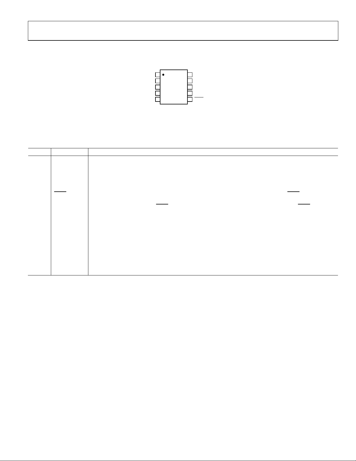
PIN CONFIGURATION AND FUNCTION DESCRIPTIONS
1
V
A
OUT
V
OUT
V
OUT
V
OUT
AD5624R/
2
B
AD5644R/
3
GND
AD5664R
4
C
TOP VIEW
(Not to Scale)
5
D
EXPOSED PAD TIED TO
GND ON LFCSP PACKAGE
10
V
REFIN/VREFOUT
9
V
DD
8
DIN
7
SCLK
6
SYNC
Figure 3. Pin Configuration
Table 7. Pin Function Descriptions
Pin No. Mnemonic Description
1 V
2 V
A Analog Output Voltage from DAC A. The output amplifier has rail-to-rail operation.
OUT
B Analog Output Voltage from DAC B. The output amplifier has rail-to-rail operation.
OUT
3 GND Ground Reference Point for all Circuitry on the Part.
4 V
5 V
6
C Analog Output Voltage from DAC C. The output amplifier has rail-to-rail operation.
OUT
D Analog Output Voltage from DAC D. The output amplifier has rail-to-rail operation.
OUT
Active Low Control Input. This is the frame synchronization signal for the input data. When SYNC goes low, it
SYNC
powers on the SCLK and DIN buffers and enables the input shift register. Data is transferred in on the falling
edges of the next 24 clocks. If SYNC is taken high before the 24th falling edge, the rising edge of SYNC acts as an
interrupt and the write sequence is ignored by the device.
7 SCLK
Serial Clock Input. Data is clocked into the input shift register on the falling edge of the serial clock input. Data
can be transferred at rates up to 50 MHz.
8 DIN
Serial Data Input. This device has a 24-bit shift register. Data is clocked into the register on the falling edge of the
serial clock input.
9 VDD
Power Supply Input. These parts can be operated from 2.7 V to 5.5 V, and the supply should be decoupled with a
10 μF capacitor in parallel with a 0.1 μF capacitor to GND.
10 V
REFIN/VREFOUT
The AD5624R/AD5644R/AD5664R have a common pin for reference input and reference output. When using the
internal reference, this is the reference output pin. When using an external reference, this is the reference input
pin. The default for this pin is as a reference input.
05856-003
Rev. B | Page 9 of 28
Page 10

AD5624R/AD5644R/AD5664R
TYPICAL PERFORMANCE CHARACTERISTICS
10
VDD = V
8
T
6
4
2
0
–2
INL ERROR (LSB)
–4
–6
–8
–10
0 5k 10k 15k 20k 25k 30k 35k 40k 45k 50k 55k 60k 65k
= 25°C
A
REF
= 5V
CODE
Figure 4. AD5664R INL, External Reference
05856-004
1.0
VDD = V
T
0.8
0.6
0.4
0.2
0
–0.2
DNL ERROR (LSB)
–0.4
–0.6
–0.8
–1.0
0 10k 20k 30k 40k 50k 60k
= 25°C
A
REF
= 5V
CODE
Figure 7. AD5664R DNL, External Reference
05856-007
4
VDD = V
T
3
2
1
0
–1
INL ERROR (LSB)
–2
–3
–4
0 2500 5000 75 00 10000 12500 15000
= 25°C
A
REF
= 5V
CODE
Figure 5. AD5644R INL, External Reference
1.0
VDD = V
T
0.8
0.6
0.4
0.2
0
–0.2
INL ERROR (LSB)
–0.4
–0.6
–0.8
–1.0
0 500 1000 1500 2000 2500 3000 3500 4000
= 25°C
A
REF
= 5V
CODE
Figure 6. AD5624R INL, External Reference
0.5
VDD = V
T
0.4
0.3
0.2
0.1
0
–0.1
DNL ERROR (LSB)
–0.2
–0.3
–0.4
05856-005
–0.5
0 2500 5000 7500 10000 12500 15000
= 25°C
A
REF
= 5V
05856-008
CODE
Figure 8. AD5644R DNL, External Reference
0.20
VDD = V
T
0.15
0.10
0.05
0
–0.05
DNL ERROR (LSB)
–0.10
–0.15
05856-006
–0.20
0 500 1000 1500 2000 2500 3000 35 00 4000
= 25°C
A
REF
= 5V
05856-009
CODE
Figure 9. AD5624R DNL, External Reference
Rev. B | Page 10 of 28
Page 11

AD5624R/AD5644R/AD5664R
10
VDD = 5V
8
V
= 2.5V
REFOUT
TA = 25°C
6
4
2
0
–2
INL ERROR (LSB)
–4
–6
–8
–10
0
5000
10000
CODE
50000
45000
40000
35000
30000
25000
20000
15000
65000
60000
55000
05856-010
Figure 10. AD5664R-5 INL, Internal Reference
4
VDD=5V
=2.5V
V
REFOUT
3
TA= 25°C
2
1
0
–1
INL ERROR (LSB)
–2
–3
–4
0
8750
7500
6250
5000
3750
2500
1250
CODE
11250
12500
10000
16250
15000
13750
05856-011
Figure 11. AD5644R-5 INL, Internal Reference
1.0
VDD=5V
0.8
0.6
0.4
0.2
0
–0.2
DNL ERROR (LSB)
–0.4
–0.6
–0.8
–1.0
0
V
REFOUT
TA=25°C
5000
=2.5V
10000
15000
20000
25000
30000
CODE
Figure 13. AD5664R-5 DNL, Internal Reference
0.5
VDD = 5V
0.4
V
= 2.5V
REFOUT
TA = 25°C
0.3
0.2
0.1
0
–0.1
DNL ERRO R (LSB)
–0.2
–0.3
–0.4
–0.5
0
1250
2500
3750
5000
6250
7500
CODE
Figure 14. AD5644R-5 DNL, Internal Reference
35000
8750
40000
10000
45000
11250
50000
12500
55000
13750
60000
15000
05856-013
65000
05856-014
16250
1.0
VDD=5V
=2.5V
V
0.8
REFOUT
= 25°C
T
A
0.6
0.4
0.2
0
–0.2
INL ER ROR (LS B)
–0.4
–0.6
–0.8
–1.0
0 1000500 20001500 350030002500 4000
CODE
Figure 12. AD5624R-5 INL, Internal Reference
05856-012
Rev. B | Page 11 of 28
0.20
VDD = 5V
V
= 2.5V
REFOUT
0.15
TA = 25°C
0.10
0.05
0
–0.05
DNL ERRO R (LSB)
–0.10
–0.15
–0.20
0 1000500 20001500 350030002500 4000
CODE
Figure 15. AD5624R-5 DNL, Internal Reference
05856-015
Page 12

AD5624R/AD5644R/AD5664R
10
VDD = 3V
8
V
= 1.25V
REFOUT
T
= 25°C
A
6
4
2
0
–2
INL ERROR (LSB)
–4
–6
–8
–10
0
5000
10000
CODE
40000
35000
30000
25000
20000
15000
55000
50000
45000
05856-016
65000
60000
Figure 16. AD5664R-3 INL, Internal Reference
4
VDD = 3V
V
= 1.25V
REFOUT
3
T
= 25°C
A
2
1
0
–1
INL ERROR (LSB)
–2
–3
–4
0
1250
2500
3750
5000
6250
7500
CODE
8750
11250
13750
12500
10000
05856-017
16250
15000
Figure 17. AD5644R-3 INL, Internal Reference
1.0
VDD = 3V
0.8
V
= 1.25V
REFOUT
T
= 25°C
A
0.6
0.4
0.2
0
–0.2
DNL ERROR (LSB)
–0.4
–0.6
–0.8
–1.0
0
5000
10000
CODE
50000
45000
40000
35000
30000
25000
20000
15000
65000
60000
55000
05856-019
Figure 19. AD5664R-3 DNL, Internal Reference
0.5
VDD = 3V
0.4
V
= 1.25V
REFOUT
T
= 25°C
A
0.3
0.2
0.1
0
–0.1
DNL ERROR (LSB)
–0.2
–0.3
–0.4
–0.5
0
1250
2500
3750
5000
6250
7500
CODE
8750
11250
12500
10000
16250
15000
13750
05856-020
Figure 20. AD5644R-3 DNL, Internal Reference
1.0
VDD = 3V
0.8
V
= 1.25V
REFOUT
T
= 25°C
A
0.6
0.4
0.2
0
–0.2
INL ERROR (LSB)
–0.4
–0.6
–0.8
–1.0
0 500 1000 1500 2000 2500 3000 3500 4000
CODE
Figure 18. AD5624R-3 INL, Internal Reference
05856-018
Rev. B | Page 12 of 28
0.20
VDD = 3V
V
= 1.25V
REFOUT
0.15
T
= 25°C
A
0.10
0.05
0
–0.05
DNL ERROR (LSB)
–0.10
–0.15
–0.20
0 500 1000 1500 2000 2500 3000 3500 4000
CODE
Figure 21. AD5624R-3 DNL, Internal Reference
05856-021
Page 13

AD5624R/AD5644R/AD5664R
8
6
= V
V
4
2
0
ERROR (LSB)
–2
–4
–6
–8
–40 –20 40200 1008060
= 5V
DD
REF
TEMPERATURE (°C)
Figure 22. INL Error and DNL Error vs. Temperature
10
8
6
= 5V
V
DD
4
= 25°C
T
A
2
0
–2
ERROR (LSB)
–4
–6
–8
–10
0.75 1.25 1.75 2. 25 4.253.753.252.75 4.75
V
(V)
REF
Figure 23. INL Error and DNL Error vs. V
MAX INL
MAX DNL
MIN DNL
MIN INL
05856-022
MAX INL
MAX DNL
MIN DNL
MIN INL
05856-023
REF
0
VDD = 5V
–0.02
–0.04
–0.06
–0.08
–0.10
–0.12
ERROR (% F SR)
–0.14
–0.16
–0.18
–0.20
–40 –20 40200 1008060
GAIN ERROR
FULL-SCAL E ERROR
TEMPERATURE (°C)
05856-025
Figure 25. Gain Error and Full-Scale Error vs. Temperature
1.5
1.0
0.5
0
–0.5
ERROR (mV)
–1.0
–1.5
–2.0
–2.5
–40 –20 40200860 1000
ZERO-SCALE ERROR
OFFSET ERROR
TEMPERATURE (°C)
05856-026
Figure 26. Zero-Scale Error and Offset Error vs. Temperature
8
6
T
= 25°C
A
4
2
0
ERROR (LSB)
–2
–4
–6
–8
2.7 3. 2 3.7 4. 74.2 5.2
VDD (V)
Figure 24. INL Error and DNL Error vs. Supply
MAX INL
MAX DNL
MIN DNL
MIN INL
05856-024
Rev. B | Page 13 of 28
1.0
0.5
GAIN ERROR
0
–0.5
ERROR (% FSR)
–1.0
–1.5
–2.0
FULL-SCALE ERROR
2.7 3.2 3. 7 4.74.2 5.2
VDD (V)
Figure 27. Gain Error and Full-Scale Error vs. Supply
05856-027
Page 14

AD5624R/AD5644R/AD5664R
C
C
1.0
= 25°C
T
A
0.5
0
–0.5
–1.0
ERROR (mV)
–1.5
ZERO-SCALE ERROR
8
VDD= 3.6V
T
= 25°C
A
7
6
5
4
FREQUENCY
3
2
–2.0
–2.5
2.7 3.2 4.23.7 5.24.7
VDD (V)
OFFSET ERROR
Figure 28. Zero-Scale Error and Offset Error vs. Supply
VDD= 5.5V
6
= 25°C
T
A
5
Y
4
3
FREQUEN
2
1
0
0.41 0.42 0.43 0.44 0.45
IDD (mA)
Figure 29. IDD Histogram with External Reference, 5.5 V
1
0
0.39 0.40 0.41 0.42 0. 43
05856-028
Figure 31. I
8
VDD= 3.6V
T
7
6
5
4
FREQUENCY
3
2
1
05856-029
0
Histogram with External Reference, 3.6 V
DD
= 25°C
A
0.90
Figure 32. IDD Histogram with Internal Reference, V
IDD (mA)
0.92 0.94 0.96
IDD (mA)
REFOUT
= 1.25 V
05856-060
05856-061
6
VDD= 5.5V
= 25°C
T
A
5
4
Y
3
FREQUEN
2
1
0
0.92 0.94 0.96 0.98
IDD (mA)
Figure 30. IDD Histogram with Internal Reference, V
REFOUT
05856-030
= 2.5 V
0.5
DAC LOADED WIT H
FULL-SCAL E
0.4
SOURCING CURRENT
0.3
0.2
VDD= 3V
0.1
V
= 1.25V
REFOUT
0
–0.1
ERROR VOLTAGE (V)
–0.2
–0.3
–0.4
–0.5
–10 –8 –6 –4 –2 0 2 4 8610
VDD= 5V
V
REFOUT
= 2.5V
CURRENT (mA)
DAC LOADED WIT H
ZERO-SCALE
SINKING CURRENT
Figure 33. Headroom at Rails vs. Source and Sink
5856-031
Rev. B | Page 14 of 28
Page 15

AD5624R/AD5644R/AD5664R
6
VDD= 5V
V
= 2.5V
REFOUT
5
T
= 25°C
A
4
3
(V)
OUT
V
2
1
0
–1
–30 –20 –10 0 10 20 30
CURRENT (mA)
Figure 34. AD56x4R-5 Source and Sink Capability
4
VDD= 3V
V
= 1.25V
REFOUT
T
= 25°C
A
3
2
(V)
OUT
V
1
3/4 SCALE
MIDSCALE
1/4 SCALE
FULL SCALE
3/4 SCALE
MIDSCALE
1/4 SCALE
ZERO SCALE
FULL SCALE
V
OUT
= 909mV/DIV
VDD = V
T
FULL-SCALE CODE CHANGE
0x0000 TO 0xFFFF
OUTPUT LOADED WITH 2kΩ
AND 200pF TO GND
= 25°C
A
REF
= 5V
1
5856-046
TIME BASE = 4µs/DIV
05856-048
Figure 37. Full-Scale Settling Time, 5 V
VDD = V
T
V
1
DD
= 25°C
A
REF
= 5V
0
–1
–30 –20 –10 0 10 20 30
CURRENT (mA)
ZERO SCALE
Figure 35. AD56x4R-3 Source and Sink Capability
0.50
0.45
0.40
0.35
0.30
0.25
(mA)
DD
I
0.20
0.15
0.10
0.05
TA = 25°C
0
–40 –20 0 20 40 60 80 100
V
= V
DD
REFIN
= V
V
DD
REFIN
TEMPERATURE ( °C)
= 5V
= 3V
Figure 36. Supply Current vs. Temperature
MAX(C2)
2
5856-047
V
OUT
CH1 2.0V CH2 500mV M100µs 125MS/ s
A CH1 1.28V
420.0mV
8.0ns/pt
05856-049
Figure 38. Power-On Reset to 0 V
SYNC
1
3
SCLK
V
OUT
VDD = 5V
2
CH1 5.0V
05856-063
CH3 5.0V
CH2 500mV M400ns A CH1 1.4V
05856-050
Figure 39. Exiting Power-Down to Midscale
Rev. B | Page 15 of 28
Page 16

AD5624R/AD5644R/AD5664R
2.538
2.537
2.536
2.535
2.534
2.533
2.532
2.531
(V)
2.530
2.529
OUT
V
2.528
2.527
2.526
2.525
2.524
2.523
2.522
2.521
0 50 100 150 350 400200 250 300 450 512
VDD= V
T
5ns/SAMPL E NUMBER
GLITCH IMPULSE = 9.494nV
1LSB CHANGE AROUND
MIDSCALE (0x8000 TO 0x7FFF)
SAMPLE NUMBER
= 25°C
A
REF
= 5V
Figure 40. Digital-to-Analog Glitch Impulse (Negative)
05856-058
VDD = V
T
DAC LOADED WITH MIDSCALE
1
Y AXIS = 2µV/DIV
X AXIS = 4s/DIV
= 25°C
A
REF
= 5V
Figure 43. 0.1 Hz to 10 Hz Output Noise Plot, External Reference
05856-051
2.498
2.497
2.496
2.495
(V)
OUT
V
2.494
2.493
2.492
2.491
0 50 100 150 350 400200 250 300 450 512
VDD= V
T
5ns/SAMPL E NUMBER
ANALOG CROS STALK = 0.424nV
SAMPLE NUMBER
= 25°C
A
REF
= 5V
Figure 41. Analog Crosstalk, External Reference
2.496
2.494
2.492
2.490
2.488
2.486
2.484
2.482
2.480
2.478
(V)
2.476
OUT
2.474
V
2.472
2.470
2.468
2.466
2.464
2.462
2.460
2.458
2.456
0 50 100 150 350 400200 250 300 450 512
VDD= 5V
= 2.5V
V
REFOUT
= 25°C
T
A
5ns/SAMPL E NUMBER
ANALOG CROS STALK = 4.462nV
SAMPLE NUMBER
Figure 42. Analog Crosstalk, 2.5 V Internal Reference
VDD = 5V
V
= 2.5V
REFOUT
= 25°C
T
A
DAC LOADED WITH MIDSCALE
1
10µV/DIV
05856-059
5s/DIV
05856-052
Figure 44. 0.1 Hz to 10 Hz Output Noise Plot, 2.5 V Internal Reference
VDD = 3V
= 1.25V
V
REFOUT
= 25°C
T
A
DAC LOADED WITH MIDSCALE
1
5µV/DIV
05856-062
4s/DIV
05856-053
Figure 45. 0.1 Hz to 10 Hz Output Noise Plot, 1.25 V Internal Reference
Rev. B | Page 16 of 28
Page 17

AD5624R/AD5644R/AD5664R
–
800
TA = 25°C
MIDSCALE LO ADED
700
600
500
16
14
12
V
= V
REF
TA = 25°C
DD
V
3V
=
DD
400
300
OUTPUT NOISE (nV/ √Hz)
200
VDD= 3V
100
V
REFOUT
0
100 10k1k 100k 1M
= 1.25V
VDD= 5V
V
= 2.5V
REFOUT
FREQUENCY ( Hz)
5856-054
10
TIME (µs)
8
6
4
012 34567 9810
CAPACITANCE (nF)
Figure 46. Noise Spectral Density, Internal Reference Figure 48. Settling Time vs. Capacitive Load
20
VDD = 5V
T
= 25°C
A
–30
DAC LOADED WIT H FULL SCALE
V
= 2V ± 0.3V p -p
REF
–40
–50
–60
–70
AMPLITUDE ( dB)
–80
–90
–100
2k 4k 6k 8k 10k
Figure 47. Total Harmonic Distortion
FREQUENCY ( Hz)
5856-055
5
0
–5
–10
–15
–20
AMPLITUDE ( dB)
–25
–30
–35
–40
10k 100k 1M 10M
FREQUENCY (Hz)
Figure 49. Multiplying Bandwidth
V
5V
=
DD
5856-056
VDD = 5V
T
= 25°C
A
05856-057
Rev. B | Page 17 of 28
Page 18

AD5624R/AD5644R/AD5664R
TERMINOLOGY
Relative Accuracy or Integral Nonlinearity (INL)
For the DAC, relative accuracy or integral nonlinearity is a
measurement of the maximum deviation, in LSBs, from a
straight line passing through the endpoints of the DAC transfer
function. A typical INL vs. code plot can be seen in Figure 4.
Differential Nonlinearity (DNL)
Differential nonlinearity is the difference between the measured
change and the ideal 1 LSB change between any two adjacent
codes. A specified differential nonlinearity of ±1 LSB maximum
ensures monotonicity. This DAC is guaranteed monotonic by
design. A typical DNL vs. code plot can be seen in Figure 7.
Zero-Code Error
Zero-scale error is a measurement of the output error when
zero code (0x0000) is loaded to the DAC register. Ideally, the
output should be 0 V. The zero-code error is always positive in
the AD5664R because the output of the DAC cannot go below
0 V due to a combination of the offset errors in the DAC and
the output amplifier. Zero-code error is expressed in mV. A plot
of zero-code error vs. temperature can be seen in Figure 26.
Full-Scale Error
Full-scale error is a measurement of the output error when fullscale code (0xFFFF) is loaded to the DAC register. Ideally, the
output should be V
− 1 LSB. Full-scale error is expressed in
DD
percent of full-scale range. A plot of full-scale error vs.
temperature can be seen in Figure 25.
Gain Error
This is a measure of the span error of the DAC. It is the deviation
in slope of the DAC transfer characteristic from the ideal
expressed as % of FSR.
Zero-Code Error Drift
This is a measurement of the change in zero-code error with a
change in temperature. It is expressed in µV/°C.
Gain Temperature Coefficient
This is a measurement of the change in gain error with changes
in temperature. It is expressed in ppm of FSR/°C.
Offset Error
Offset error is a measure of the difference between V
and V
(ideal) expressed in mV in the linear region of the
OUT
(actual)
OUT
transfer function. Offset error is measured on the AD5664R
with code 512 loaded in the DAC register. It can be negative or
positive.
DC Power Supply Rejection Ratio (PSRR)
This indicates how the output of the DAC is affected by changes
in the supply voltage. PSRR is the ratio of the change in V
a change in V
in dB. V
for full-scale output of the DAC. It is measured
DD
is held at 2 V, and VDD is varied by ±10%.
REF
OUT
to
Output Voltage Settling Time
This is the amount of time it takes for the output of a DAC to
settle to a specified level for a ¼ to ¾ full-scale input change
and is measured from the 24
th
falling edge of SCLK.
Digital-to-Analog Glitch Impulse
Digital-to-analog glitch impulse is the impulse injected into the
analog output when the input code in the DAC register changes
state. It is normally specified as the area of the glitch in nV-s,
and is measured when the digital input code is changed by
1 LSB at the major carry transition (0x7FFF to 0x8000) (see
Figure 40).
Digital Feedthrough
Digital feedthrough is a measure of the impulse injected into
the analog output of the DAC from the digital inputs of the
DAC, but is measured when the DAC output is not updated. It
is specified in nV-s, and measured with a full-scale code change
on the data bus, that is, from all 0s to all 1s and vice versa.
Reference Feedthrough
Reference feedthrough is the ratio of the amplitude of the signal
at the DAC output to the reference input when the DAC output
is not being updated. It is expressed in dB.
Noise Spectral Density
This is a measurement of the internally generated random
noise. Random noise is characterized as a spectral density
(nV/√Hz). It is measured by loading the DAC to midscale and
measuring noise at the output. It is measured in nV/√Hz. A plot
of noise spectral density can be seen in Figure 46.
DC Crosstalk
DC crosstalk is the dc change in the output level of one DAC in
response to a change in the output of another DAC. It is
measured with a full-scale output change on one DAC (or soft
power-down and power-up) while monitoring another DAC kept
at midscale. It is expressed in V.
DC crosstalk due to load current change is a measure of the
impact that a change in load current on one DAC has to
another DAC kept at midscale. It is expressed in V/mA.
Digital Crosstalk
This is the glitch impulse transferred to the output of one DAC
at midscale in response to a full-scale code change (all 0s to all
1s and vice versa) in the input register of another DAC. It is
measured in standalone mode and is expressed in nV-s.
Rev. B | Page 18 of 28
Page 19

AD5624R/AD5644R/AD5664R
Analog Crosstalk
This is the glitch impulse transferred to the output of one DAC
due to a change in the output of another DAC. It is measured by
loading one of the input registers with a full-scale code change
(all 0s to all 1s and vice versa). Then execute a software LDAC
and monitor the output of the DAC whose digital code was not
changed. The area of the glitch is expressed in nV-s.
DAC-to-DAC Crosstalk
This is the glitch impulse transferred to the output of one DAC
due to a digital code change and subsequent analog output
change of another DAC. It is measured by loading the attack
channel with a full-scale code change (all 0s to all 1s and vice
versa) using the command write to and update while monitoring the output of the victim channel that is at midscale. The
energy of the glitch is expressed in nV-s.
Multiplying Bandwidth
The amplifiers within the DAC have a finite bandwidth. The
multiplying bandwidth is a measure of this. A sine wave on the
reference (with full-scale code loaded to the DAC) appears on
the output. The multiplying bandwidth is the frequency at
which the output amplitude falls to 3 dB below the input.
Total Harmonic Distortion (THD)
This is the difference between an ideal sine wave and its
attenuated version using the DAC. The sine wave is used as the
reference for the DAC, and the THD is a measurement of the
harmonics present on the DAC output. It is measured in dB.
Rev. B | Page 19 of 28
Page 20

AD5624R/AD5644R/AD5664R
V
THEORY OF OPERATION
DIGITAL-TO-ANALOG SECTION
The AD5624R/AD5644R/AD5664R DACs are fabricated on a
CMOS process. The architecture consists of a string DAC
followed by an output buffer amplifier. Figure 50 shows a block
diagram of the DAC architecture.
DD
V
REFIN
RESISTOR
STRING
GND
REF
DAC
REGISTER
Figure 50. DAC Architecture
Because the input coding to the DAC is straight binary, the ideal
output voltage when using an external reference is given by
OUTPUT
AMPLIFI ER
(GAIN = +2)
V
OUT
05856-032
R
R
R
R
R
Figure 51. Resistor String
TO OUTPUT
AMPLIFIER
5856-033
OUT
VV
REFIN
⎟
⎜
N
2
⎠
⎝
D
⎞
⎛
×=
The ideal output voltage when using the internal reference is
given by
D
⎞
⎛
VV
2
××=
⎟
REFOUTOUT
⎜
N
2
⎠
⎝
where:
D is the decimal equivalent of the binary code that is loaded to
the DAC register:
0 to 4095 for AD5624R (12 bit).
0 to 16,383 for AD5644R (14 bit).
0 to 65,535 for AD5664R (16 bit).
N is the DAC resolution.
RESISTOR STRING
The resistor string is shown in Figure 51. It is simply a string of
resistors, each of value R. The code loaded to the DAC register
determines at which node on the string the voltage is tapped off
to be fed into the output amplifier. The voltage is tapped off by
closing one of the switches connecting the string to the
amplifier. Because it is a string of resistors, it is guaranteed
monotonic.
OUTPUT AMPLIFIER
The output buffer amplifier can generate rail-to-rail voltages on
its output, which gives an output range of 0 V to V
a load of 2 k in parallel with 1000 pF to GND. The source and
sink capabilities of the output amplifier can be seen in Figure 33
and Figure 34. The slew rate is 1.8 V/µs with a ¼ to ¾ full-scale
settling time of 7 µs.
. It can drive
DD
INTERNAL REFERENCE
The AD5624R/AD5644R/AD5664R on-chip reference is off at
power-up and is enabled via a write to a control register. See the
Internal Reference Setup section for details.
The AD56x4R-3 has a 1.25 V, 5 ppm/°C reference giving a fullscale output of 2.5 V. The AD56x4R-5 has a 2.5 V, 5 ppm/°C
reference giving a full-scale output of 5 V. The internal reference
associated with each part is available at the V
pin. A buffer
REFOUT
is required if the reference output is used to drive external loads.
When using the internal reference, it is recommended that a
100 nF capacitor is placed between reference output and GND
for reference stability.
EXTERNAL REFERENCE
The V
use of an external reference if the application requires it. The
default condition of the on-chip reference is off at power-up. All
devices (AD56x4R-3 and the AD56x4R-5) can be operated from
a single 2.7 V to 5.5 V supply.
pin on the AD56x4R-3 and AD56x4R-5 allows the
REFIN
SERIAL INTERFACE
The AD5624R/AD5644R/AD5664R have a 3-wire serial interface
SYNC
, SCLK, and DIN) that is compatible with SPI, QSPI, and
(
MICROWIRE interface standards as well as with most DSPs. See
for a timing diagram of a typical write sequence. Figure 2
SYNC
The write sequence begins by bringing the
from the DIN line is clocked into the 24-bit shift register on the
falling edge of SCLK. The serial clock frequency can be as high
as 50 MHz, making the AD5624R/AD5644R/AD5664R compatible with high speed DSPs. On the 24
th
falling clock edge, the
last data bit is clocked in and the programmed function is
executed, that is, a change in DAC register contents and/or a
change in the mode of operation.
line low. Data
Rev. B | Page 20 of 28
Page 21

AD5624R/AD5644R/AD5664R
SYNC
At this stage, the
either case, it must be brought high for a minimum of 15 ns before
the next write sequence so that a falling edge of
the next write sequence.
Because the
than it does when V
between write sequences for even lower power operation. As
mentioned previously, it must, however, be brought high again
just before the next write sequence.
INPUT SHIFT REGISTER
The input shift register is 24 bits wide (see Figure 52). The first
two bits are don’t care bits. The next three are the command
bits, C2 to C0 (see Table 8), followed by the 3-bit DAC address,
A2 to A0 (see Table 9 ), and then the 16-, 14-, 12-bit data-word.
The data-word comprises the 16-, 14-, 12-bit input code
followed by 0, 2, or 4 don’t care bits, for the AD5664R,
AD5644R, and AD5624R, respectively (see Figure 52, Figure 53,
and Figure 54). These data bits are transferred to the DAC
register on the 24
SYNC
line can be kept low or be brought high. In
Table 8. Command Definition
C2 C1 C0 Command
SYNC
can initiate
0 0 0 Write to input register n
0 0 1 Update DAC register n
SYNC
buffer draws more current when VIN = 2 V
= 0.8 V,
IN
SYNC
should be idled low
0 1 0
0 1 1
1 0 0
1 0 1
1 1 0
Write to input register n, update all
(software LDAC)
Write to and update DAC channel n
Power down DAC (power-up)
Reset
LDAC register setup
1 1 1 Internal reference setup (on/off)
Table 9. Address Command
A2 A1 A0 Address (n)
0 0 0 DAC A
0 0 1 DAC B
th
falling edge of SCLK.
0 1 0
0 1 1
1 1 1 All DACs
DAC C
DAC D
SYNC INTERRUPT
In a normal write sequence, the
24 falling edges of SCLK, and the DAC is updated on the 24
falling edge. However, if
falling edge, then this acts as an interrupt to the write sequence.
The input shift register is reset and the write sequence is seen as
invalid. Neither an update of the DAC register contents nor a
change in the operating mode occurs (see ). Figure 55
DB23 (MSB) DB0 (LSB)
X X C2 C1 C0 A2 A1 A0 D15 D14 D13 D12 D11 D10 D9 D8 D7 D6 D5 D4 D3 D2 D1 D0
DATA BIT S
COMMAND BITS ADDRESS BITS
Figure 52. AD5664R Input Shift Register Contents
DB23 (MSB) DB0 (LSB)
X X C2 C1 C0 A2 A1 A0 XXD11 D10D13 D12 D9 D8 D7 D6 D5 D4 D3 D2 D1 D0
DATA BITS
COMMAND BITS ADDRESS BITS
Figure 53. AD5644R Input Shift Register Contents
DB23 (MSB) DB0 (LSB)
X X C2 C1 C0 A2 A1 A0 XXXXD11 D10 D9 D8 D7 D6 D5 D4 D3 D2 D1 D0
DATA BITS
COMMAND BITS ADDRESS BITS
Figure 54. AD5624R Input Shift Register Contents
SYNC
line is kept low for at least
SYNC
is brought high before the 24th
th
05856-034
05856-035
05856-036
SCLK
DIN
DB23 DB23 DB0DB0
INVALID WRITE SEQUENCE:
SYNC HIG H BEFO RE 24
TH
FALLING EDGE
Figure 55.
SYNC
Rev. B | Page 21 of 28
VALID WRIT E SEQUENCE, OUT PUT UPDATES
Interrupt Facility
ON THE 24
TH
FALLING EDGE
05856-037
Page 22

AD5624R/AD5644R/AD5664R
POWER-ON RESET
The AD5624R/AD5644R/AD5664R family contains a power-on
reset circuit that controls the output voltage during power-up.
The output of the AD5624R/AD5644R/AD5664R DACs powers
up to 0 V and the output remains there until a valid write
sequence is made to the DACs. This is useful in applications
where it is important to know the state of the output of the
DACs while they are in the process of powering up.
SOFTWARE RESET
The AD5624R/AD5644R/AD5664R contain a software reset
function. Command 101 is reserved for the software reset
function (see Tab le 8). The software reset command contains
two reset modes that are software programmable by setting bit
DB0 in the control register.
Table 10 shows how the state of the bit corresponds to the
software reset modes of operation of the devices.
Table 12 shows the contents of the input shift register during the
software reset mode of operation.
Table 10. Software Reset Modes for the
AD5624R/AD5644R/AD5664R
DB0 Registers Reset to 0
0 DAC register
Input shift register
1 (Power-On Reset) DAC register
Input shift register
LDAC register
Power-down register
Internal reference setup register
POWER-DOWN MODES
The AD5624R/AD5644R/AD5664R contain four separate modes
of operation. Command 100 is reserved for the power-down
function (see Tab le 8). These modes are software programmable
by setting two bits (DB5 and DB4) in the control register. Tab le 11
shows how the state of the bits corresponds to the mode of
operation of the device. All DACs (DAC D to DAC A) can be
powered down to the selected mode by setting the corresponding four bits (DB3, DB2, DB1, and DB0) to 1.
By executing the same Command 100, any combination of DACs
can be powered up by setting the bits (DB5 and DB4) to normal
operation mode. To select which combination of DAC channels
to power-up, set the corresponding four bits (DB3, DB2, DB1,
and DB0) to 1. See Table 13 for contents of the input shift register
during power-down/power-up operation.
Table 11.
AD5664R
DB5 DB4 Operating Mode
0 0 Normal operation
0 1 Power-down mode: 1 kΩ to GND
1 0 Power-down mode: 100 kΩ to GND
1 1 Power-down mode: three-state
Modes of Operation for the AD5624R/AD5644R/
When Bit DB5 and Bit DB4 are set to 0, the part works normally
with its normal power consumption of 450 µA at 5 V. However,
for the three power-down modes, the supply current falls to
480 nA at 5 V (200 nA at 3 V). Not only does the supply current
fall, but the output stage is also internally switched from the
output of the amplifier to a resistor network of known values.
This allows the output impedance of the part to be known while
the part is in power-down mode. The outputs can either be
connected internally to GND through a 1 k resistor, or left
open-circuited (three-state) as shown in Figure 56.
RESISTOR
STRING DAC
Figure 56. Output Stage During Power-Down
AMPLIFIER
POWER-DOW N
CIRCUITRY
RESISTOR
NETWORK
V
OUT
05856-038
The bias generator, the output amplifier, the resistor string, and
other associated linear circuitry are shutdown when power-down
mode is activated. However, the contents of the DAC register are
unaffected when in power-down. The time to exit power-down
is typically 4 µs for V
= 5 V and for VDD = 3 V (see Figure 39).
DD
Table 12. 24-Bit Input Shift Register Contents for Software Reset Command
DB23 to DB22 (MSB) DB21 DB20 DB19 DB18 DB17 DB16 DB15 to DB1 DB0 (LSB)
x 1 0 1 x x x x 1/0
Don’t care Command bits (C2 to C0) Address bits (A2 to A0) Don’t care Determines software reset mode
Table 13. 24-Bit Input Shift Register Contents of Power-Down/Power-Up Operation for the AD5624R/AD5644R/AD5664R
DB23 to
DB22
(MSB) DB21 DB20 DB19 DB18 DB17 DB16
x 1 0 0 x x x x PD1 PD0 DAC D DAC C DAC B DAC A
Don’t
care
Command bits (C2 to C0) Address bits (A2 to A0)
Don’t care
Rev. B | Page 22 of 28
DB15
to DB6 DB5 DB4 DB3 DB2 DB1
Don’t
care
Power- down
mode
Power-down/power-up channel
selection, set bit to 1 to select channel
DB0
(LSB)
Page 23

AD5624R/AD5644R/AD5664R
LDAC FUNCTION
The AD5624R/AD5644R/AD5664R DACs have doublebuffered interfaces consisting of two banks of registers: input
registers and DAC registers. The input registers are connected
directly to the input shift register and the digital code is tra
ferred to the relevant input register on completion of a valid
write sequence. The DAC registers contain the digital code u
by the resistor strings.
The double-buffered int
erface is useful if the user requires
simultaneous updating of all DAC outputs. The user can write
to three of the input registers individually and then write to t
remaining input register, updating all DAC registers simultaneously. Command 010 is reserved for this software LDAC.
Access to the DAC registers is
controlled by the LDAC function.
The LDAC register contains two modes of operation for ea
DAC channel. The DAC channels are selected by setting th
bits of the 4-bit LDAC register (DB3, DB2, DB1, a
nd DB0).
Command 110 is reserved for setting up the LDAC register.
When the LDAC bit register is set lo
registers are latched and the input register
without affecting the contents of the DAC r
bit register is set hiLDAC
e transparent and t ut registers are
com
nsferred to them on th
tra e falling edge of the 24
This is equivalent to g an
nently low for the se DAC channel, that
gh, however, the DAC
havin
lected is, synchronous
pdate mode. See Table 1 ster mode of
peration. See Table 16 fo hift register
o r contents of the input s
uring the LDAC register
d setup command.
w, the corresponding DAC
s can change state
egisters. When the
registers
the inpbe he contents of
th
SCLK pulse.
LDAC
hardware pin tied perma-
regiu 4 for the LDAC
ns-
ch
e
sed
he
This flexibility is useful in applications where the user wants to
update select channels simultaneously, while the rest of the
channels update synchronously.
Table 14. LDAC Register Mode of Operation
LDAC Bits
(DB3 to DB0) LDAC Mode of O
0
1
INTERN L REF
Th p r ce is off at power-up by default. This
A ERENCE SETUP
e on-chi eferen reference
Normal operation (default), DAC register
update is controlled by write command.
The DAC registers are updated after new
data is read in on the falling edge of the
th
SCLK puls
24
peration
e.
can be turned on or off by setting a software programmable bit,
DB0, in the control register. Table 15 shows how the state of the
bit corresponds to the mode of operation. Command 111 is
reserved for setting up the internal reference (see Tabl e 8).
Table 16 shows how the state of the bits in the input shift
register corresponds to the mode of operation of the device
during internal reference setup.
Table 15. Reference Setup Register
Internal Reference
Setup Register
(DB0) Action
0 Reference off (default)
1 Reference on
Table 16. 24-Bit Input Shift Register Contents for LDAC Setu
DB23 to DB22
(MSB)
x 1 1 0 x x x x DAC D DAC C DAC B DAC A
Don’t care
DB21 DB20 DB19 DB18 DB17 DB15 to DB4 DB3 DB2 DB1 DB0 (LSB)
Command bits
(C2 to C0)
Address b
(A2 to A0); don
Table 17. 24-Bit Input Shift Register Contents for Internal Re
DB23 to DB22
SB)
(M
x 1 1 1 x x x x 1/0
Don’t care Command bits (C2 to C0) Address bits (A2 to A0) Don’t care Reference setup register
DB21 DB20 DB19 DB18 DB17 DB16 DB15 to DB1 DB0 (LSB)
p Command for the AD5624R/AD5644R/AD5664R
DB16
its
’t care
Don’t care
Set bit to 0 or 1 for required mode of
operation on respective channel
ference Setup Command
Rev. B | Page 23 of 28
Page 24

AD5624R/AD5644R/AD5664R
MICROPROCESSO
AD5624R/AD5644R/AD5664R to Blackfin ADSP-BF
R INTERFACING
53x
Interface
Figure 57 shows a serial interface between the AD5624R/
AD5644R/AD5664R and the Blackfin® ADSP-BF53x microprocessor. The ADSP-BF53x processor family incorporates tw
dual-channel synchronous serial ports, SPORT1 and SPORT0,
for serial and multiproc
to connect to the AD5624R/AD5644R/AD5664R, the setup
essor communications. Using SPORT0
for
the interface is that the DT0PRI drives the DIN pin of the
AD5624R/AD5644R/AD5664R, while TSCLK0 drives the
SYNC
SCLK of the part. The
ADSP-BF53x
TFS0
1
ADDITIONAL PINS OMIT TED FO R CLARITY.
Figure 57. Blackfin ADSP-BF53x Interface to AD5624R/AD5644R/AD566
is driven from TFS0.
1
AD5624R/
AD5644R/
AD5664R
SYNC
DINDTOP RI
SCLKTSCLK0
1
05856-039
4R
AD5624R/AD5644R/AD5664R to 68HC11/68L11 Interface
Figure 58 shows a serial interface between the AD5624R/
AD5644R/AD5664R and the 68HC11/68L11 microcontroller.
SCK of the 68HC11/68L11 drives the SCLK of the AD5624R/
AD5644R/AD5664R, while the MOSI output drives the serial
data line of the DAC.
SYNC
The
onditions for correct operation of this interface are that the
c
68H
CPHA bit as 1. When data is transmitted to the DAC, the
line is taken low
as descri
lid on the falling ge of S . Seria ta from he 68H 1/
va ed CK l da t C1
68L11 is tra -bit bytes with o
edges occurring in the tran ta is tran
signal is derived from a port line (PC7). The setup
C11/68L11 is configured with its CPOL bit as 0 and its
(PC7). When the 68HC11/68L11 is configured
bed previo ta in M utp
usly, da appear g on the OSI o ut is
nsmitted in 8 nly eight fallin
smit cycle. Da
smitted MSB
g clock
SYNC
first. To load data to the AD5624R/AD5644R/AD5664R, PC7 is
left low after the first eight bits are transferred, and a second
serial write oper
high at t s proced .
he end of thi ure
Figure 58. 68HC11/68L11 Interface to AD5624R/AD5644R/AD5664R
ation is performed to the DAC; PC7 is taken
68HC11/68L11
1
ADDITIONAL PINS OMITTED FOR CL ARITY.
1
PC7
AD5624R/
AD5644R/
AD5664R
SYNC
SCLKSCK
DINMOSI
1
05856-040
o
AD5624R/AD5644R/AD5664R to 80C51/80L51 Interface
Figure 59 shows a serial interface between the AD5624R/
AD5644R/AD5664R and the 80C51
setup for the interface is that the TxD of the 80C51
AD5624R/AD5644R/AD5664R, while RSCLK of the
serial data line o t. The
rammable pin on th
prog e port. In this case, port line P3.3 is used.
When data is transmitted
.3 is taken low. The 80
P3 C51/80L51 transmits data in 8-bit bytes
only; thus, only eight fall
To load data to the DAC, er the first eight bits are
f the par
to the AD5624R/AD5644R/AD5664R,
ing clock edges occur in the transmit cycle.
P3.3 is left low aft
transmitted, and a second write cycle is in
second byte of data. P3.3 is taken high foll
/80L51 microcontroller. The
/80L51 drives
SYNC
signal is derived from a bit-
itiated to transmit the
owing the completion of
xD drives the
this cycle. The 80C51/80L51 outputs the serial data in LSB first
format. The AD5624R/AD5644R/AD5664R must receive data with
the MSB first. The 80C51/80L51 transmit routine should take this
into account.
80C51/80L51
1
ADDITIONAL
ure 59. 80C51/80L5 to AD5624R/AD5644R/AD5664R
Fig 1 Interface
5624R/AD5644R/ IRE Interface
AD AD5664R to MICROW
gure 60 shows an inter he AD5624R/AD5644R/
Fi face between t
D5664R and any MICROWIRE-compatible device. Serial data
A
1
P3.3
PINS OMIT TED FOR CL ARITY.
AD5624R/
AD5644R/
AD5664R
SYNC
SCLKTxD
DINRxD
1
05856-041
is shifted out on the falling edge of the serial clock and is
clocked into the AD5624R/AD5644R/AD5664R on the rising
edge of the SK.
MICROWIRE
1
ADDITIONAL PINS OMITTED FOR CL ARITY.
Figure 60. MICROWIRE Interface to AD5624R/AD5644R/AD5664R
1
CS
AD5624R/
644R
AD5 /
664R
AD5
SYNC
SCLKSK
DINSO
1
05856-042
Rev. B | Page 24 of 28
Page 25

AD5624R/AD5644R/AD5664R
V
APPLICATIONS
USING A REFERENCE AS A POWER SUPPLY FOR THE AD5624R/AD5644R/AD5664R
Because the supply current required by the AD5624R/AD5644R/
AD5664R is extremely low, an alternative option is to use a
voltage reference to supply the required voltage to the part (see
Figure 61). This is especially useful if the power supply is quite
noisy, or if the system supply voltages are at some value other
than 5 V or 3 V, for example, 15 V. The voltage reference outputs
a steady supply voltage for the AD5624R/AD5644R/AD5664R
(see Figure 59). If the low dropout REF195 is used, it must
supply 450 μA of current to the AD5624R/AD5644R/AD5664R
with no load on the output of the DAC. When the DAC output
is loaded, the REF195 also needs to supply the current to the
load. The total current required (with a 5 kΩ load on the DAC
output) is
450 μA + (5 V/5 kΩ) = 1.45 mA
The load regulation of the REF195 is typically 2 ppm/mA,
resulting in a 2.9 ppm (14.5 μV) error for the 1.45 mA current
drawn from it. This corresponds to a 0.191 LSB error.
15
REF195
3-WIRE
SERIAL
INTERFACE
Figure 61. REF195 as Power Supply to the AD5624R/AD5644R/AD5664R
SYNC
SCLK
DIN
5V
V
DD
AD5624R/
AD5644R/
AD5664R
V
OUT
= 0V TO 5V
05856-043
R2 = 10kΩ
+5V
0.1µF10µF
Figure 62. Bipolar Operation with the AD5624R/AD5644R/AD5664R
R1 = 10kΩ
V
DDVOUT
AD5624R/
AD5644R/
AD5664R
3-WIRE
SERIAL
INTERFACE
+5V
AD820/
OP295
–5V
±5V
05856-044
USING AD5624R/AD5644R/AD5664R WITH A GALVANICALLY ISOLATED INTERFACE
In process control applications in industrial environments, it is
often necessary to use a galvanically isolated interface to protect
and isolate the controlling circuitry from any hazardous commonmode voltages that might occur in the area where the DAC is
functioning. Isocouplers provide isolation in excess of 3 kV. The
AD5624R/AD5644R/AD5664R use a 3-wire serial logic interface,
so the ADuM130x 3-channel digital isolator provides the
required isolation (see Figure 63). The power supply to the part
also needs to be isolated, which is done by using a transformer.
On the DAC side of the transformer, a 5 V regulator provides
the 5 V supply required for the AD5624R/AD5644R/AD5664R.
5V
POWER
REGULATOR
10µF
0.1µF
BIPOLAR OPERATION USING THE AD5624R/AD5644R/AD5664R
The AD5624R/AD5644R/AD5664R have been designed for
single-supply operation, but a bipolar output range is also
possible using the circuit in Figure 62. The circuit gives an
output voltage range of ±5 V. Rail-to-rail operation at the
amplifier output is achievable using an AD820 or an OP295 as
the output amplifier.
The output voltage for any input code can be calculated as
follows:
⎡
⎛
×=
VV
⎜
⎢
OUT
⎣
where
D represents the input code in decimal (0 to 65,536).
With V
= 5 V, R1 = R2 = 10 kΩ,
DD
10
OUT
⎛
⎜
⎝
V
×=D
536,65
536,65
⎝
⎞
V5
−
⎟
⎠
+
⎞
×
⎟
⎠
R2R1D
R1
⎞
V
⎟
DDDD
⎠
⎛
⎜
⎝
This is an output voltage range of ±5 V, with 0x0000 corresponding to a −5 V output, and 0xFFFF corresponding to a
+5 V output.
⎤
R2
⎞
⎛
×−
⎟
⎜
⎥
R1
⎠
⎝
⎦
Rev. B | Page 25 of 28
V
SCLK
DATA
Figure 63. AD5624R/AD5644R/AD5664R with a Galvanically Isolated Interface
SDI
V
IA
ADuM1300
V
IB
V
IC
V
OA
V
OB
V
OC
SCLK
SYNC
AD5624R/
AD5644R/
AD5664R
DIN
GND
DD
V
OUT
05856-045
Page 26

AD5624R/AD5644R/AD5664R
POWER SUPPLY BY
When accuracy is important in a circuit, it is helpful to carefull
consider the power supply and ground return layout on the
board. The printed circuit board containing th
AD5644R/AD5664R should have separate analog and digital
sections, each having its own area of the board. If the AD5624R/
AD5644R/AD5664R are in a system where other devices require
an AGND-to-DGND connection, the connection should be
made at one point only. This ground point should be as close as
possible to the AD5624R/AD5644R/AD5664R.
The power supply to the AD5624R/AD5644R/AD5664R should
be bypassed with 10 µF and 0.1 µF capacitors. The capacitors
should be located as close as possible to the device, with the
0.1 µF capacitor ideally right up against the device. The 10 µF
capacitor is the tantalum bead type. It is important that the
0.1 µF capacitor have low effective series resistance (ESR) and
effective se
ries inductance (ESI), for example, common ceramic
PASSING AND GROUNDING
y
e AD5624R/
types of capacitors. This 0.1 µF capacitor provides a low impedance path to ground for high frequencies caused by transient
currents due to internal logic switching.
The power supply line itself should have as large a trace as
possible to provide a low impedance path and to reduce glitch
effects on the supply line. Clocks and other fast switching
digital signals should be shielded from other parts of the board
by digital ground. Avoid crossover of digital and analog signals
if possible. When traces cross on opposite sides of the board,
ensure that they run at right angles to each other to reduce
feedthrough effects through the board. The best board layout
technique is the microstrip technique where the component
side
of the board is dedicated to the ground plane only and the
signal traces are placed on the solder side. However, this is
always possible with a 2-layer board.
not
Rev. B | Page 26 of 28
Page 27

AD5624R/AD5644R/AD5664R
OUTLINE DIMENSIONS
3.00
BSC SQ
0.30
0.23
0.18
0.50 BSC
PIN 1 INDEX
AREA
0.80
0.75
0.70
SEATING
PLANE
TOP VIEW
0.80 MAX
0.55 NOM
0.50
0.40
0.30
0.05 MAX
0.02 NOM
0.20 REF
6
EXPOSED
(BOTTOM VIEW)
5
PAD
2.48
2.38
2.23
10
1.74
1.64
1.49
1
P
N
I
1
R
A
O
T
N
I
D
C
I
)
0
2
.
R
0
(
031208-B
Figure 64. 10-Lead Lead Frame Chip Scale Package [LFCSP_WD]
3 mm × 3 mm Body, Very Very Thin, Dual Lead
(CP-10-9)
Dimensions shown in millimeters
3.10
3.00
2.90
6
10
3.10
3.00
2.90
1
PIN 1
0.50 BSC
0.95
0.85
0.75
0.15
0.05
0.33
0.17
COPLANARITY
0.10
COMPLIANT TO JEDEC STANDARDS MO-187-BA
Figure 65. 10-Lead Mini Small Outline Package [MSOP]
5.15
4.90
4.65
5
1.10 MAX
SEATING
PLANE
0.23
0.08
8°
0°
(RM-10)
Dimensions shown in millimeters
0.80
0.60
0.40
Rev. B | Page 27 of 28
Page 28

AD5624R/AD5644R/AD5664R
ORDERING GUIDE
Package
odel Temperature Ra Ac
M nge curacy Internal Reference
AD5624RBCPZ-3R2
AD5624RBCPZ-3REEL7
AD5624RBCPZ-5R2
AD5624RBCPZ-5REEL7
AD5624RBRMZ-3
AD5624RBRMZ-3REEL7
AD5624RBRMZ-5
AD5624RBRMZ-5REEL7
AD5644RBRMZ-3
AD5644RBRMZ-3REEL7
AD5644RBRMZ-5
AD5644RBRMZ-5REEL7
AD5664RBCPZ-3R2
AD5664RBCPZ-3REEL7
AD5664RBRMZ-3
AD5664RBRMZ-3REEL7
AD5664RBRMZ-5
AD5664RBRMZ-5REEL7
EVAL-AD5664REBZ
1
Z = RoHS Compliant Part.
1
1
−40°C to +105°C ±1 LSB INL 2.5 V 10-Lead LFCSP_WD CP-10-9 DBZ
1
−40°C to +105°C ±1 LSB INL 1.25 V 10-Lead MSOP RM-10 D7L
1
−40°C to +105°C ±1 LSB INL 2.5 V 10-Lead MSOP RM-10 D7V
1
−40°C to +105°C ±4 LSB INL 1.25 V 10-Lead MSOP RM-10 D7E
1
−40°C to +105°C ±4 LSB INL 2.5 V 10-Lead MSOP RM-10 D7D
1
−40°C to +105°C ±16 LSB INL 1.25 V 10-Lead LFCSP_WD CP-10-9 D73
1
−40°C to +105°C ±16 LSB INL 1.25 V 10-Lead MSOP RM-10 D73
1
−40°C to +105°C ±16 LSB INL 10-Lead MSOP RM-10 D75 2.5 V
1
Evaluation Board
−40°C to +105°C ±1 LSB INL 1.25 V 10-Lead LFCSP_WD CP-10-9 D7L
1
−40°C to +105°C ±1 LSB INL 1.25 V 10-Lead LFCSP_WD CP-10-9 D7L
1
−40°C to +105°C ±1 LSB INL 2.5 V 10-Lead LFCSP_WD CP-10-9 DBZ
1
−40°C to +105°C ±1 LSB INL 1.25 V 10-Lead MSOP RM-10 D7L
1
−40°C to +105°C ±1 LSB INL 2.5 V 10-Lead MSOP RM-10 D7V
1
−40°C to +105°C ±4 LSB INL 1.25 V 10-Lead MSOP RM-10 D7E
1
−40°C to +105°C ±4 LSB INL 2.5 V 10-Lead MSOP RM-10 D7D
1
−40°C to +105°C ±16 LSB INL 1.25 V 10-Lead LFCSP_WD CP-10-9 D73
1
−40°C to +105 ad MSOP RM-10 D73 °C ±16 LSB INL 1.25 V 10-Le
1
−40°C to +105°C ± 10-Lead MSOP RM-10 D75 16 LSB INL 2.5 V
Description
Package
Option Branding
©2006–2008 Analog Devices, Inc. All rights reserved. Trademarks and
registered trademarks are the property of their respective owners.
D05856-0-4/08(B)
Rev. B | Page 28 of 28
 Loading...