

Page 1
CONTROL
AMP
BAND -
GAP
REFERENCE
AD558
OUTPUT
AMP
8-BIT VOLTAGE-SWITCHING
D-TO-A CONVERTER
MSB
I2L LATCHES
I2L
CONTROL
LOGIC
LSB
V
OUT
V
OUT
SENSE A
V
OUT
SELECT
GND
+V
CC
MSB
GND CS CE
LSB
CONTROL
INPUTS
DB0
DB1
DB2
DB3
DB4
DB5
DB6
DB7
DIGITAL INPUT DATA (BUS)
DACPORT Low Cost, Complete
a
FEATURES
Complete 8-Bit DAC
Voltage Output–2 Calibrated Ranges
Internal Precision Bandgap Reference
Single-Supply Operation: +5 V to +15 V
Full Microprocessor Interface
Fast: 1 ms Voltage Settling to 61/2 LSB
Low Power: 75 mW
No User Trims
Guaranteed Monotonic Over Temperature
MIN
to T
MAX
2
L), an extremely dense
All Errors Specified T
Small 16-Pin DIP and 20-Pin PLCC Packages
Single Laser-Wafer-Trimmed Chip for Hybrids
Low Cost
MIL-STD-883 Compliant Versions Available
PRODUCT DESCRIPTION
The AD558 DACPORT® is a complete voltage-output 8-bit
digital-to-analog converter, including output amplifier, full
microprocessor interface and precision voltage reference on a
single monolithic chip. No external components or trims are
required to interface, with full accuracy, an 8-bit data bus to an
analog system.
The performance and versatility of the DACPORT is a result of
several recently-developed monolithic bipolar technologies. The
complete microprocessor interface and control logic is implemented with integrated injection logic (I
and low power logic structure that is process-compatible with
linear bipolar fabrication. The internal precision voltage reference
is the patented low voltage bandgap circuit which permits fullaccuracy performance on a single +5 V to +15 V power supply.
Thin-film silicon-chromium resistors provide the stability required for guaranteed monotonic operation over the entire operating temperature range (all grades), while recent advances in
laser-wafer-trimming of these thin-film resistors permit absolute
calibration at the factory to within ± 1 LSB; thus no user-trims
for gain or offset are required. A new circuit design provides
voltage settling to ±1/2 LSB for a full-scale step in 800 ns.
The AD558 is available in four performance grades. The AD558J
and K are specified for use over the 0°C to +70°C temperature
range, while the AD558S and T grades are specified for –55°C
to +125°C operation. The “J” and “K” grades are available
either in 16-pin plastic (N) or hermetic ceramic (D) DIPS.
They are also available in 20-pin JEDEC standard PLCC packages. The “S” and “T” grades are available in the 16-pin hermetic ceramic DIP package.
*Protected by U.S. Patent Nos. 3,887,863; 3,685,045; 4,323,795; Patents
Pending.
DACPORT is a registered trademark of Analog Devices, Inc.
REV. A
Information furnished by Analog Devices is believed to be accurate and
reliable. However, no responsibility is assumed by Analog Devices for its
use, nor for any infringements of patents or other rights of third parties
which may result from its use. No license is granted by implication or
otherwise under any patent or patent rights of Analog Devices.
µP-Compatible 8-Bit DAC
AD558*
FUNCTIONAL BLOCK DIAGRAM
PRODUCT HIGHLIGHTS
1. The 8-bit I2L input register and fully microprocessorcompatible control logic allow the AD558 to be directly
connected to 8- or 16-bit data buses and operated with
standard control signals. The latch may be disabled for
direct DAC interfacing.
2. The laser-trimmed on-chip SiCr thin-film resistors are
calibrated for absolute accuracy and linearity at the factory.
Therefore, no user trims are necessary for full rated accuracy
over the operating temperature range.
3. The inclusion of a precision low voltage bandgap reference
eliminates the need to specify and apply a separate reference source.
4. The voltage switching structure of the AD558 DAC section
along with a high speed output amplifier and laser trimmed
resistors give the user a choice of 0 V to +2.56 V or 0 V to
+10 V output ranges, selectable by pin-strapping. Circuitry is
internally compensated for minimum settling time on both
ranges; typically settling to ± 1/2 LSB for a full-scale 2.55 volt
step in 800 ns.
5. The AD558 is designed and specified to operate from a
single +4.5 V to +16.5 V power supply.
6. Low digital input currents, 100 µA max, minimize bus load-
ing. Input thresholds are TTL/low voltage CMOS compatible over the entire operating V
7. All AD558 grades are available in chip form with guaranteed
specifications from +25°C to T
visual inspection is standard on Analog Devices bipolar
chips. Contact the factory for additional chip information.
8. The AD558 is available in versions compliant with MILSTD-883. Refer to Analog Devices Military Products Databook or current AD558/883B data sheet for detailed
specifications.
One Technology Way, P.O. Box 9106, Norwood, MA 02062-9106, U.S.A.
Tel: 617/329-4700 Fax: 617/326-8703
range.
CC
. MIL-STD-883, Class B
MAX
Page 2

AD558–SPECIFICATIONS
Model AD558J AD558K AD558S
(@ TA = +258C, VCC = +5 V to +15 V unless otherwise noted)
1
AD558T
1
Min Typ Max Min Typ Max Min Typ Max Min Typ Max Units
RESOLUTION 8 8 8 8 Bits
RELATIVE ACCURACY
2
0°C to +70°C ±1/2 ±1/4 ±1/2 ±1/4 LSB
–55°C to +125°C ±3/4 ±3/8 LSB
OUTPUT
3
Ranges
0 to +2.56 0 to +2.56 0 to +2.56 0 to +2.56 V
0 to +10 0 to +10 0 to +10 0 to +10 V
Current Source +5 +5 +5 +5 mA
Sink Internal Passive Internal Passive Internal Passive Internal Passive
Pull-Down to Ground
OUTPUT SETTLING TIME
0 to 2.56 Volt Range 0.8 1.5 0.8 1.5 0.8 1.5 0.8 1.5 µs
0 to 10 Volt Range
FULL-SCALE ACCURACY
5
4
6
2.0 3.0 2.0 3.0 2.0 3.0 2.0 3.0 µs
4
Pull-Down to Ground Pull-Down to Ground Pull-Down to Ground
@ 25°C 61.5 60.5 61.5 60.5 LSB
T
MIN
to T
MAX
62.5 61 62.5 61 LSB
ZERO ERROR
@ 25°C 61 61/2 61 61/2 LSB
T
to T
MIN
MAX
MONOTONICITY
T
to T
MIN
MAX
7
Guaranteed Guaranteed Guaranteed Guaranteed
62 61 62 61 LSB
DIGITAL INPUTS
to T
T
MIN
Input Current ±100 ±100 ±100 100 µA
MAX
Data Inputs, Voltage
Bit On-Logic “1” 2.0 2.0 2.0 2.0 V
Bit On-Logic “0” 0 0.8 0 0 0 V
Control Inputs, Voltage
On-Logic “1” 2.0 2.0 2.0 2.0 V
On-Logic “0” 0 0.8 0 0.8 0 0.8 0 0.8 V
Input Capacitance 4 4 4 4 pF
8
TIMING
tW, Strobe Pulse Width 200 200 200 200 ns
to T
T
MIN
MIN
MIN
to T
to T
MAX
MAX
MAX
Data Hold Time 10 10 10 10 ns
t
DH
T
Data Set-Up Time 200 200 200 200 ns
t
DS
T
270 270 270 270 ns
10 10 10 10 ns
270 270 270 270 ns
POWER SUPPLY
Operating Voltage Range (V
2.56 Volt Range +4.5 +16.5 +4.5 +16.5 +4.5 +16.5 +4.5 +16.5 V
)
CC
10 Volt Range +11.4 +16.5 +11.4 +16.5 +11.4 +16.5 +11.4 +16.5 V
Current (I
Rejection Ratio 0.03 0.03 0.03 0.03 %/%
POWER DISSIPATION, V
)1525 15 25 15 25 15 25 mA
CC
= 5 V 75 125 75 125 75 125 75 125 mW
CC
VCC = 15 V 225 375 225 375 225 375 225 375 mW
OPERATING TEMPERATURE RANGE 0 +70 0 +70 –55 +125 –55 +125 °C
NOTES
1
The AD558 S & T grades are available processed and screened lo MIL-STD-883 Class B. Consult Analog Devices’ Military Databook for details.
2
Relative Accuracy is defined as the deviation of the code transition points from the ideal transfer point on a straight line from the offset to the full scale of the device.
See “Measuring Offset Error”.
3
Operation of the 0 volt to 10 volt output range requires a minimum supply voltage of +11.4 volts.
4
Passive pull-down resistance is 2 kΩ for 2.56 volt range, 10 kΩ for 10 volt range.
5
Settling time is specified for a positive-going full-scale step to ± 1/2 LSB. Negative-going steps to zero are slower, but can be improved with an external pull-down.
6
The full range output voltage for the 2.56 range is 2.55 V and is guaranteed with a +5 V supply, for the 10 V range, it is 9.960 V guaranteed with a +15 V supply.
7
A monotonic converter has a maximum differential linearity error of ± 1 LSB.
8
See Figure 7.
Specifications shown in boldface are tested on all production units at final electrical test.
Specifications subject to change without notice.
–2–
REV. A
Page 3
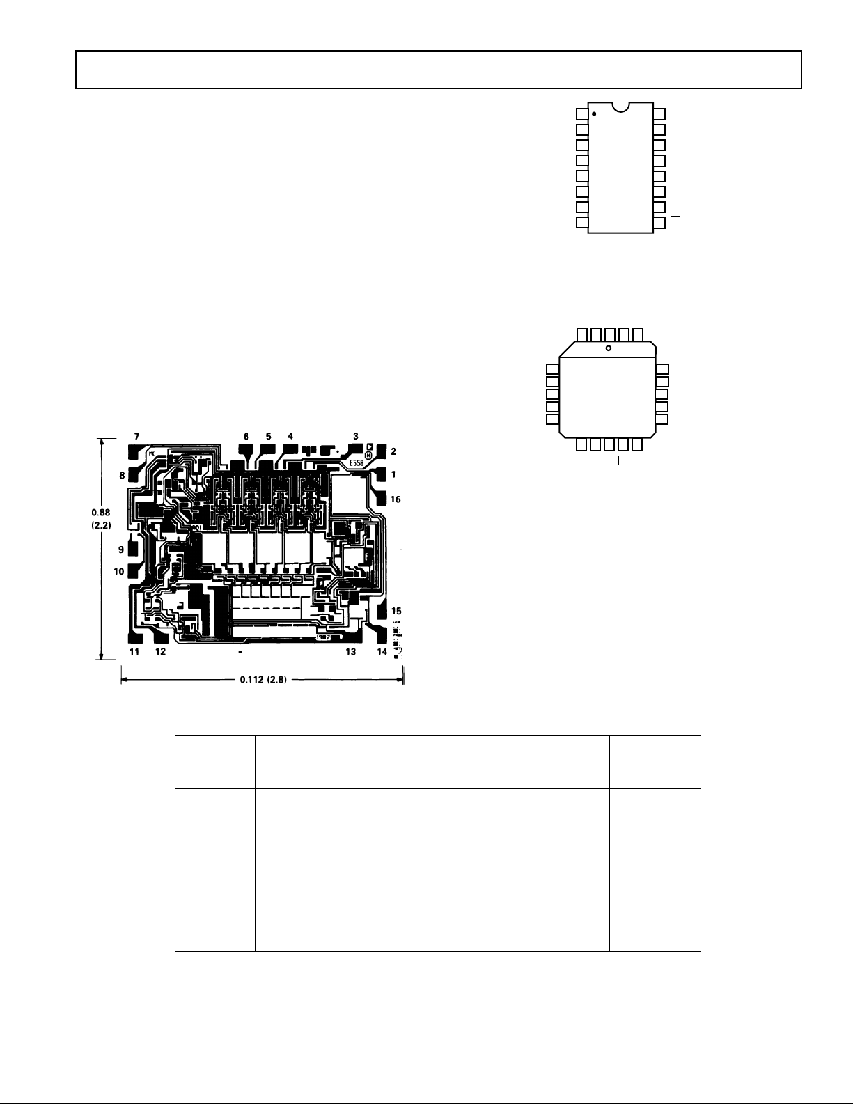
ABSOLUTE MAXIMUM RATINGS*
1
2
3
4
5
6
7
8
16
15
14
13
12
11
10
9
AD558
TOP VIEW
(Not to Scale)
V
OUT
V
OUT
SENSE
V
OUT
SELECT
GND
GND
+V
CC
CS
(LSB) DB0
DB1
DB2
DB3
DB4
DB5
DB6
(MSB) DB7
CE
VCC to Ground . . . . . . . . . . . . . . . . . . . . . . . . . . . 0 V to +18 V
Digital Inputs (Pins 1–10) . . . . . . . . . . . . . . . . . .0 V to +7.0 V
V
. . . . . . . . . . . . . . . . . . . . . . . Indefinite Short to Ground
OUT
Momentary Short to V
CC
Power Dissipation . . . . . . . . . . . . . . . . . . . . . . . . . . . .450 mW
Storage Temperature Range
N/P (Plastic) Packages . . . . . . . . . . . . . . . . –25°C to +100°C
D (Ceramic) Package . . . . . . . . . . . . . . . . .–55°C to +150°C
Lead Temperature (soldering, 10 sec) . . . . . . . . . . . . . +300°C
Thermal Resistance
Junction to Ambient/Junction to Case
D (Ceramic) Package . . . . . . . . . . . . . . 100°C/W/30°C/W
N/P (Plastic) Packages . . . . . . . . . . . . . 140°C/W/55°C/W
*Stresses greater than those listed under “Absolute Maximum Ratings” may cause
permanent damage to the device. This is a stress rating only and functional
operation of the device at these or any other conditions above those indicated in the
operational section of this specification is not implied. Exposure to absolute
maximum rating conditions for extended periods may affect device reliability.
AD558 METALIZATION PHOTOGRAPH
Dimensions shown in inches and (mm).
Figure 1a. AD558 Pin Configuration (DIP)
AD558
Figure 1a. AD558 Pin Configuration (DIP)
SENSE
OUT
OUT
NC
V
DB0 (LSB)
1
20 19
NC
CE
(MSB) DB7
V
V
SELECT
18
OUT
GND
17
16
NC
15
GND
+V
14
CC
CS
NC = NO CONNECT
DB1
2
3
4
DB2
5
DB3
NC
DB4
DB5
6
7
8
AD558
TOP VIEW
(Not to Scale)
9
10 11 12 13
DB6
Figure 1b. AD558 Pin Configuration (PLCC and LCC)
REV. A
ORDERING GUIDE
Relative Accuracy Full-Scale
Error Max Error, Max Package
MIN
to T
MAX
T
to T
MIN
MAX
Option
2
Model
1
Temperature T
AD558JN 0°C to +70°C ±1/2 LSB ±2.5 LSB Plastic (N-16)
AD558JP 0°C to +70°C ±1/2 LSB ±2.5 LSB PLCC (P-20A)
AD558JD 0°C to +70°C ±1/2 LSB ±2.5 LSB TO-116 (D-16)
AD558KN 0°C to +70°C ±1/4 LSB ±1 LSB Plastic (N-16)
AD558KP 0°C to +70°C ±1/4 LSB ±1 LSB PLCC (P-20A)
AD558KD 0°C to +70°C ±1/4 LSB ±1 LSB TO-116 (D-16)
AD558SD –55°C to +125°C ±3/4 LSB ±2.5 LSB TO-116 (D-16)
AD558TD –55°C to +125°C ±3/8 LSB ±1 LSB TO-116 (D-16)
NOTES
1
For details on grade and package offerings screened in accordance with MIL-STD-883, refer to the Analog Devices
Military Products Databook or current AD558/883B data sheet.
2
D = Ceramic DIP; N = Plastic DIP; P = Plastic Leaded Chip Carrier.
–3–
Page 4

AD558
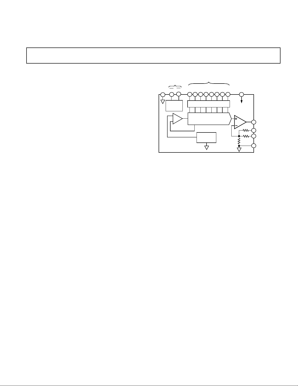
CIRCUIT DESCRIPTION
The AD558 consists of four major functional blocks, fabricated
on a single monolithic chip (see Figure 2). The main D-to-A
converter section uses eight equally-weighted laser-trimmed
current sources switched into a silicon-chromium thin-film
R/2R resistor ladder network to give a direct but unbuffered 0
mV to 400 mV output range. The transistors that form the
DAC switches are PNPs; this allows direct positive-voltage logic
interface and a zero-based output range.
CONTROL
CONTROL
BAND-
GAP
REFERENCE
INPUTS
CS CE
I2L
LOGIC
CONTROL
AMP
DIGITAL INPUT DATA
LSB
DB1
DB0
DB2
DB4
DB3
DB5
I2L LATCHES
8-BIT VOLTAGE-SWITCHING
D-TO-A CONVERTER
MSB
DB6
DB7
+V
CC
OUTPUT
AMP
GND GND
V
V
OUT
V
OUT
OUT
SENSE
SELECT
Figure 2. AD558 Functional Block Diagram
The high speed output buffer amplifier is operated in the noninverting mode with gain determined by the user-connections
at the output range select pin. The gain-setting application
resistors are thin-film laser-trimmed to match and track the
DAC resistors and to assure precise initial calibration of the two
output ranges, 0 V to 2.56 V and 0 V to 10 V. The amplifier
output stage is an NPN transistor with passive pull-down for
zero-based output capability with a single power supply. The
internal precision voltage reference is of the patented bandgap
type. This design produces a reference voltage of 1.2 volts and
thus, unlike 6.3 volt temperature compensated Zeners, may be
operated from a single, low voltage logic power supply. The
microprocessor interface logic consists of an 8-bit data latch and
control circuitry. Low power, small geometry and high speed
are advantages of the I
2
L design as applied to this section. I2L is
bipolar process compatible so that the performance of the analog sections need not be compromised to provide on-chip logic
capabilities. The control logic allows the latches to be operated
from a decoded microprocessor address and write signal. If the
application does not involve a µP or data bus, wiring
CS and
CE to ground renders the latches “transparent” for direct DAC
access.
MIL-STD-883
The rigors of the military/aerospace environment, temperature
extremes, humidity, mechanical stress, etc., demand the utmost
in electronic circuits. The AD558, with the inherent reliability
of integrated circuit construction, was designed with these applications in mind. The hermetically-sealed, low profile DIP
package takes up a fraction of the space required by equivalent
modular designs and protects the chip from hazardous environments. To further ensure reliability, military temperature range
AD558 grades S and T are available screened to MIL-STD-883.
For more complete data sheet information consult the Analog
Devices’ Military Databook.
CHIP AVAILABILITY
The AD558 is available in laser-trimmed, passivated chip form.
AD558J and AD558T chips are available. Consult the factory
for details.
Input Logic Coding
Digital Input Code Output Voltage
Binary Hexadecimal Decimal 2.56 V Range 10.000 V Range
0000 0000 00 0 0 0
0000 0001 01 1 0.010 V 0.039 V
0000 0010 02 2 0.020 V 0.078 V
0000 1111 0F 15 0.150 V 0.586 V
0001 0000 10 16 0.160 V 0.625 V
0111 1111 7F 127 1.270 V 4.961 V
1000 0000 80 128 1.280 V 5.000 V
1100 0000 C0 192 1.920 V 7.500 V
1111 1111 FF 255 2.55 V 9.961 V
CONNECTING THE AD558
The AD558 has been configured for ease of application. All reference, output amplifier and logic connections are made internally. In addition, all calibration trims are performed at the
factory assuring specified accuracy without user trims. The only
connection decision that must be made by the user is a single
jumper to select output voltage range. Clean circuit board layout is facilitated by isolating all digital bit inputs on one side of
the package; analog outputs are on the opposite side.
Figure 3 shows the two alternative output range connections.
The 0 V to 2.56 V range may be selected for use with any power
supply between +4.5 V and +16.5 V. The 0 V to 10 V range
requires a power supply of +11.4 V to +16.5 V.
OUTPUT
AMP
V
V
OUT
OUT
GND
V
OUT
SENSE
SELECT
16
15
14
13
OUTPUT
AMP
V
V
OUT
OUT
GND
V
OUT
SENSE
SELECT
16
15
14
13
a. 0 V to 2.56 V Output Range b. 0 V to 10 V Output Range
Figure 3. Connection Diagrams
Because of its precise factory calibration, the AD558 is intended
to be operated without user trims for gain and offset; therefore
no provisions have been made for such user trims. If a small increase in scale is required, however, it may be accomplished
by slightly altering the effective gain of the output buffer. A
resistor in series with V
SENSE will increase the output
OUT
range.
For example if a 0 V to 10.24 V output range is desired (40 mV
= 1 LSB), a nominal resistance of 850 Ω is required. It must be
remembered that, although the internal resistors all ratiomatch and track, the absolute tolerance of these resistors is
typically ±20% and the absolute TC is typically –50 ppm/°C
(0 to –100 ppm/°C). That must be considered when rescaling is
performed. Figure 4 shows the recommended circuitry for a
full-scale output range of 10.24 volts. Internal resistance values
shown are nominal.
–4–
REV. A
Page 5

Applications–AD558
OUTPUT
AMP
604Ω
V
OUT
40kΩ
2kΩ
14kΩ
16
500Ω
15
14
13
GND
Figure 4. 10.24 V Full-Scale Connection
NOTE: Decreasing the scale by putting a resistor in series with GND
will not work properly due to the code-dependent currents in GND.
Adjusting offset by injecting dc at GND is not recommended for the
same reason.
GROUNDING AND BYPASSING*
All precision converter products require careful application of
good grounding practices to maintain full rated performance.
Because the AD558 is intended for application in microcomputer systems where digital noise is prevalent, special care must
be taken to assure that its inherent precision is realized.
The AD558 has two ground (common) pins; this minimizes
ground drops and noise in the analog signal path. Figure 5
shows how the ground connections should be made.
OUTPUT
AMP
V
OUT
16
SENSE
V
OUT
15
V
SELECT
OUT
14
GND
13
12
GND
11
+V
CC
(SEE NEXT
PAGE)
TO SYSTEM GND
TO SYSTEM GND
(SEE TEXT)
0.1µF
TO SYSTEM V
R
L
CC
The only consideration in selecting a supply voltage is that, in
order to be able to use the 0 V to 10 V output range, the power
supply voltage must be between +11.4 V and +16.5 V. If, however, the 0 V to 2.56 V range is to be used, power consumption
will be minimized by utilizing the lowest available supply voltage
(above +4.5 V).
TIMING AND CONTROL
The AD558 has data input latches that simplify interface to 8and 16-bit data buses. These latches are controlled by Chip
Enable (
CE) and Chip Select (CS) inputs. CE and CS are internally “NORed” so that the latches transmit input data to the
DAC section when both
CE and CS are at Logic “0”. If the application does not involve a data bus, a “00” condition allows
for direct operation of the DAC. When either
CE or CS go to
Logic “1”, the input data is latched into the registers and held
until both
CE and CS return to “0”. (Unused CE or CS inputs
should be tied to ground.) The truth table is given in Table I.
The logic function is also shown in Figure 6.
Table I. AD558 Control Logic Truth Table
Latch
Input Data CE CS DAC Data Condition
0 0 0 0 “Transparent”
1 0 0 1 “Transparent”
0 g 0 0 Latching
1 g 0 1 Latching
00g0 Latching
10g1 Latching
X 1 X Previous Data Latched
X X 1 Previous Data Latched
NOTES
X = Does not matter.
g = Logic Threshold at Positive-Going Transition.
Figure 5. Recommended Grounding and Bypassing
It is often advisable to maintain separate analog and digital
grounds throughout a complete system, tying them common in
one place only. If the common tie-point is remote and accidental disconnection of that one common tie-point occurs due to
card removal with power on, a large differential voltage between
the two commons could develop. To protect devices that interface to both digital and analog parts of the system, such as the
AD558, it is recommended that common ground tie-points
should be provided at each such device. If only one system
ground can be connected directly to the AD558, it is recommended that analog common be selected.
POWER SUPPLY CONSIDERATIONS
The AD558 is designed to operate from a single positive power
supply voltage. Specified performance is achieved for any supply
voltage between +4.5 V and +16.5 V. This makes the AD558
ideal for battery-operated, portable, automotive or digital mainframe applications.
*For additional insight, “An IC Amplifier Users’ Guide to Decoupling,
Grounding and Making Things Go Right For A change,” is available
at no charge from any Analog Devices Sales Office.
REV. A
–5–
Figure 6. AD558 Control Logic Function
In a level-triggered latch such as that in the AD558 there is an
interaction between data setup and hold times and the width of
the enable pulse. In an effort to reduce the time required to test
all possible combinations in production, the AD558 is tested
with t
with t
= t
= 200 ns at 25°C and 270 ns at T
DS
W
= 10 ns at all temperatures. Failure to comply with
DH
MIN
and T
MAX
,
these specifications may result in data not being latched properly.
Figure 7 shows the timing for the data and control signals;
and
CS are identical in timing as well as in function.
CE
Page 6

AD558
14
15
16
AD558
12
13
AD589
AD544
0.01µF
0.01µF
0.01µF
–5V
–1.2V
4.7kΩ
5kΩ
4.53kΩ
–5V
INPUT CODE V
OUT
00000000 +128V
10000000 0V
11111111 –1.27V
1.5kΩ
V
O
+1.28 TO
–1.27
5kΩ
+5V
500Ω
BIPOLAR
OFFSET
ADJUST
V
IN
V
OUT
= 0V TO +2.56V
OUTPUT
AMP
16
15
14
13
AGND
V
OUT
SELECT
V
OUT
SENSE
V
OUT
–V
0.5mA
DATA
INPUTS
0.8V
CS OR CE
0.8V
DAC
V OUTPUT
t
W
= STORAGE PULSE WIDTH = 200ns MIN
t
= DATA HOLD TIME = 10ns MIN
DH
t
= DATA SETUP TIME = 200ns MIN
DS
t
= DAC OUTPUT SETTLING TIME TO ±1/2 LSB
SETTLING
t
DS
t
W
t
SETTLING
Figure 7. AD558 Timing
t
DH
2.0V
2.0V
1/2 LSB
V
OUT
AD558
16
SENSEV
OUT
15
NEGATIVE
SUPPLY
R
P-D
V
EE
R
L
= 2x V
(in kΩ)
EE
Figure 9. Improved Settling Time
available, bipolar output ranges may be achieved by suitable
output offsetting and scaling. Figure 10 shows how a ± 1.28 volt
output range may be achieved when a –5 volt power supply is
available. The offset is provided by the AD589 precision 1.2 volt
reference which will operate from a +5 volt supply. The AD544
output amplifier can provide the necessary ± 1.28 volt output
swing from ±5 volt supplies. Coding is complementary offset
binary.
USE OF V
SENSE
OUT
Separate access to the feedback resistor of the output amplifier
allows additional application versatility. Figure 8a shows how
I × R drops in long lines to remote loads may be cancelled by
putting the drops “inside the loop.” Figure 8b shows how the
separate sense may be used to provide a higher output current
by feeding back around a simple current booster.
V
OUT
12
AD558
13
GND
14
GAIN
SELECT
16
V
SENSE
OUT
15
V
0V TO +10V
R
L
OUT
a. Compensation for I× R Drops in Output Lines
V
CC
V
12
AD558
13
GND
14
GAIN
SELECT
OUT
16
V
SENSE
OUT
15
2N2222
0V TO +2.56V
R
L
V
OUT
b. Output Current Booster
Figure 8. Use of V
OUT
Sense
OPTIMIZING SETTLING TIME
In order to provide single-supply operation and zero-based
output voltage ranges, the AD558 output stage has a passive
“pull-down” to ground. As a result, settling time for negative
going output steps may be longer than for positive-going output
steps. The relative difference depends on load resistance and
capacitance. If a negative power supply is available, the
negative-going settling time may be improved by adding a pulldown resistor from the output to the negative supply as shown
in Figure 9. The value of the resistor should be such that, at
zero voltage out, current through that resistor is 0.5 mA max.
BIPOLAR OUTPUT RANGES
The AD558 was designed for operation from a single power
supply and is thus capable of providing only unipolar (0 V to
+2.56 V and 0 V to 10 V) output ranges. If a negative supply is
Figure 10. Bipolar Operation of AD558 from ±5 V Supplies
MEASURING OFFSET ERROR
One of the most commonly specified endpoint errors associated
with real-world nonideal DACs is offset error.
In most DAC testing, the offset error is measured by applying
the zero-scale code and measuring the output deviation from 0
volts. There are some DACs, like the AD558 where offset errors
may be present but not observable at the zero scale, because of
other circuit limitations (such as zero coinciding with singlesupply ground) so that a nonzero output at zero code cannot be
read as the offset error. Factors like this make testing the
AD558 a little more complicated.
By adding a pulldown resistor from the output to a negative
supply as shown in Figure 11, we can now read offset errors
at zero code that may not have been observable due to circuit
limitations. The value of the resistor should be such that, at zero
voltage out, current through the resistor is 0.5 mA max.
a. 0 V to 2.56 V Output Range
–6–
REV. A
Page 7

OUTPUT
ADDRESS BUS
DATA BUS
8080A
AD558
V
OUT
DB0–DB7
16
8
8
CE
CS
ADDRESS SELECT
PULSE LOGIC
16
MEMW
MEMW → CE
DECODED ADDRESS SELECT PULSE → CS
ADDRESS BUS
DATA BUS
1802
AD558
V
OUT
DB0–DB7
8
8
8
CE
CS
ADDRESS
LATCH
&
DECODE
8
MWR
CDP 1802: MWR → CE
DECODED ADDRESS SELECT PULSE → CS
TPA
MA 0 – 7
0
LSB
1/2
1/4
–55 –25 0 +25 +50 +75 +100 +125
o
C
ZERO
ERROR
ALL AD558
AD558S, T
1LSB = 0.39% OF FULL SCALE
–1/4
–1/2
AMP
16
V
OUT
15
V
SENSE
OUT
V
14
13
OUT
AGND
SELECT
0.5mA
–V
b. 0 V to 10 V Output Range
Figure 11. Offset Connection Diagrams
INTERFACING THE AD558 TO MICROPROCESSOR
DATA BUSES
The AD558 is configured to act like a “write only” location in
memory that may be made to coincide with a read only memory
location or with a RAM location. The latter case allows data
previously written into the DAC to be read back later via the
RAM. Address decoding is partially complete for either ROM
or RAM. Figure 12 shows interfaces for three popular microprocessor systems.
ADDRESS BUS
AD558
b. 8080A/AD558 Interface
Performance
Figure 13. Full-Scale Accuracy vs. Temperature
REV. A
6800
VMA
R/W
16
φ
2
8
R/W → CE
GATED DECODED ADDRESS → CS
ADDRESS
DECODER
DATA BUS
16
a. 6800/AD558 Interface
(typical @ +258C, VCC 6 +5 V to +15 V unless otherwise noted)
LSB
1.75
1.50
1.25
1.00
0.75
0.50
FULL
SCALE
ERROR
Performance of AD558
0.25
0
–0.25
–0.50
–0.75
–1.00
–55 –25 0 +25 +50 +75 +100 +125
1LSB = 0.39% OF FULL SCALE
ALL AD558
AD558S, T
CS
CE
AD558
DB0–DB7
8
V
OUT
c. 1802/AD558 Interface
Figure 12. Interfacing the AD558 to Microprocessors
o
C
Figure 14. Zero Drift vs. Temperature Performance
of AD558
–7–
Page 8

AD558
mA
16
14
I
CC
12
10
4 6 81012141618
V
CC
VOLTS
Figure 15. Quiescent Current vs. Power Supply
Voltage for AD558
OUTLINE DIMENSIONS
Dimensions shown in inches and (mm).
N (Plastic) Package
C558f–21–8/87
D (Ceramic) Package
Figure 16. AD558 Settling Characteristics Detail
0 V to 2.56 V Output Range Full-Scale Step
Figure 17. AD558 Settling Characteristic Detail
0 V to 10 V Output Range Full-Scale Step
P (PLCC) Package
PRINTED IN U.S.A.
Figure 18. AD558 Logic Timing
–8–
REV. A
 Loading...