

Page 1
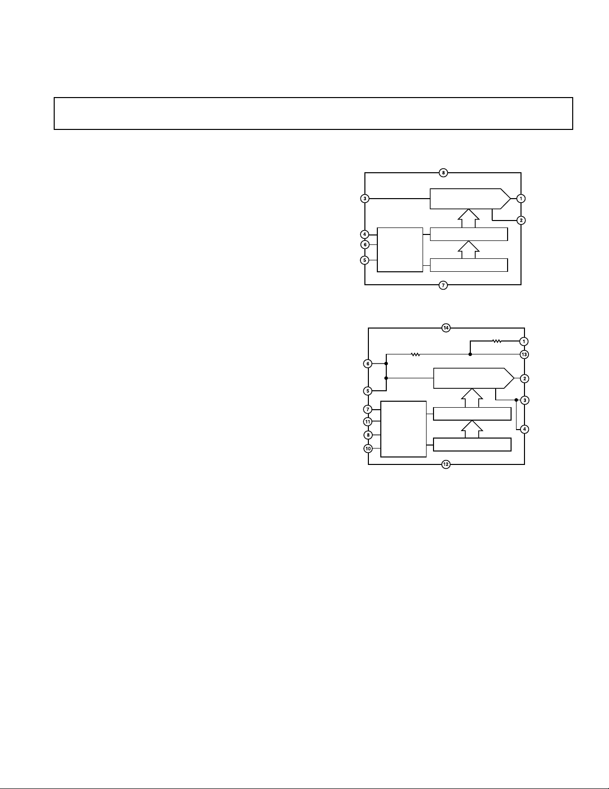
5 V, Serial-Input
SERIAL INPUT REGISTER
V
REF
CS
DIN
SCLK
AGND
V
OUT
V
DD
DGND
AD5551
14-BIT DAC
14-BIT DATA LATCH
CONTROL
LOGIC
a
FEATURES
Full 14-Bit Performance
5 V Single Supply Operation
Low Power
Fast Settling Time
Unbuffered Voltage Output Capable of Driving 60 k⍀
Loads Directly
SPI™/QSPI™/MICROWIRE™-Compatible Interface
Standards
Power-On Reset Clears DAC Output to 0 V (Unipolar
Mode)
Schmitt Trigger Inputs for Direct Optocoupler Interface
APPLICATIONS
Digital Gain and Offset Adjustment
Automatic Test Equipment
Data Acquisition Systems
Industrial Process Control
GENERAL DESCRIPTION
The AD5551 and AD5552 are single, 14-bit, serial input, voltage
output DACs that operate from a single 5 V ± 10% supply.
The AD5551 and AD5552 utilize a versatile 3-wire interface that
is compatible with SPI, QSPI, MICROWIRE, and DSP interface standards.
These DACs provide 14-bit performance without any adjustments. The DAC output is unbuffered, which reduces power
consumption and offset errors contributed by an output buffer.
With an external op amp the AD5552 can be operated in bipolar mode generating a ±V
includes Kelvin sense connections for the reference and analog
ground pins to reduce layout sensitivity. For higher precision
applications, please refer to 16-bit DACs AD5541, AD5542,
and AD5544.
The AD5551 and AD5552 are available in an SO package.
output swing. The AD5552 also
REF
Voltage-Output, 14-Bit DACs
AD5551/AD5552
FUNCTIONAL BLOCK DIAGRAMS
V
DD
R
FB
RFB
INV
V
OUT
AGNDF
AGNDS
V
REFF
V
REFS
LDAC
SCLK
DIN
AD5552
CS
R
CONTROL
LOGIC
INV
14-BIT DAC
14-BIT DATA LATCH
SERIAL INPUT REGISTER
DGND
PRODUCT HIGHLIGHTS
1. Single Supply Operation.
The AD5551 and AD5552 are fully specified and guaranteed
for a single 5 V ± 10% supply.
2. Low Power Consumption.
Typically 1.5 mW with a 5 V supply.
3. 3-Wire Serial Interface.
4. Unbuffered output capable of driving 60 kΩ loads, which
reduces power consumption as there is no internal buffer
to drive.
5. Power-On Reset Circuitry.
SPI and QSPI are trademarks of Motorola, Inc.
MICROWIRE is a trademark of National Semiconductor Corporation.
REV. 0
Information furnished by Analog Devices is believed to be accurate and
reliable. However, no responsibility is assumed by Analog Devices for its
use, nor for any infringements of patents or other rights of third parties
which may result from its use. No license is granted by implication or
otherwise under any patent or patent rights of Analog Devices.
One Technology Way, P.O. Box 9106, Norwood, MA 02062-9106, U.S.A.
Tel: 781/329-4700 World Wide Web Site: http://www.analog.com
Fax: 781/326-8703 © Analog Devices, Inc., 2000
Page 2

AD5551/AD5552–SPECIFICATIONS
(VDD = 5 V ⴞ 10%, V
TA = T
to T
MIN
MAX,
= 2.5 V, AGND = DGND = 0 V. All specifications
REF
unless otherwise noted.)
Parameter Min Typ Max Unit Test Condition
STATIC PERFORMANCE
Resolution 14 Bits
Relative Accuracy, INL ± 0.15 ± 1.0 LSB B Grade
Differential Nonlinearity ± 0.15 ± 0.8 LSB Guaranteed Monotonic
Gain Error –1.75 –0.3 0 LSB
Gain Error Temperature Coefficient ± 0.1 ppm/°C
Zero Code Error 0 0.1 0.5 LSB
Zero Code Temperature Coefficient ± 0.05 ppm/°C
AD5552
Bipolar Resistor Matching 1.000 Ω/Ω R
, Typically RFB = R
FB/RINV
= 28 kΩ
INV
± 0.0015 ± 0.0152 % Ratio Error
Bipolar Zero Offset Error ±0.25 ±2.5 LSB
Bipolar Zero Temperature Coefficient ±0.2 ppm/°C
OUTPUT CHARACTERISTICS
Output Voltage Range 0 V
–V
REF
Output Voltage Settling Time 1 µs to 1/2 LSB of FS, C
Slew Rate 25 V/µsC
– 1 LSB V Unipolar Operation
REF
V
– 1 LSB V AD5552 Bipolar Operation
REF
= 10 pF, Measured from 0% to 63%
L
= 10 pF
L
Digital-to-Analog Glitch Impulse 10 nV-s 1 LSB Change Around the Major Carry
Digital Feedthrough 10 nV-s All 1s Loaded to DAC, V
= 2.5 V
REF
DAC Output Impedance 6.25 kΩ Tolerance Typically 20%
Power Supply Rejection Ratio ± 1.0 LSB ∆VDD ± 10%
DAC REFERENCE INPUT
Reference Input Range 2.0 V
Reference Input Resistance
2
9kΩ Unipolar Operation
DD
V
7.5 kΩ AD5552, Bipolar Operation
LOGIC INPUTS
Input Current ± 1 µA
V
, Input Low Voltage 0.8 V
INL
, Input High Voltage 2.4 V
V
INH
Input Capacitance
Hysteresis Voltage
3
3
0.4 V
10 pF
REFERENCE
Reference –3 dB Bandwidth 1.3 MHz All 1s Loaded
Reference Feedthrough 1 mV p-p All 0s Loaded, V
= 1 V p-p at 100 kHz
REF
Signal-to-Noise Ratio 92 dB
Reference Input Capacitance 75 pF Code 0000
120 pF Code 3FFF
H
H
POWER REQUIREMENTS
V
DD
I
DD
4.50 5.50 V
0.3 1.1 mA
Power Dissipation 1.5 6.05 mW
NOTES
1
Temperature range is as follows: B Version: –40°C to +85°C.
2
Reference input resistance is code-dependent, minimum at 2555H.
3
Guaranteed by design, not subject to production test.
Specifications subject to change without notice.
–2–
REV. 0
Page 3
AD5551/AD5552
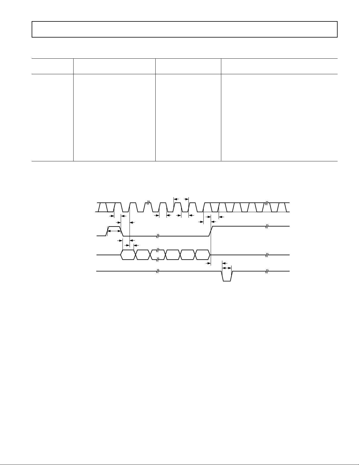
TIMING CHARACTERISTICS1,
Limit at T
MIN
, T
(VDD = 5 V ⴞ 5%, V
2
otherwise noted.)
MAX
= 2.5 V, AGND = DGND = 0 V. All specifications TA = T
REF
MIN
to T
MAX,
unless
Parameter All Versions Unit Description
f
SCLK
t
1
t
2
t
3
t
4
t
5
t
6
t
7
t
8
t
9
t
10
t
11
t
12
NOTES
1
Guaranteed by design. Not production tested.
2
Sample tested during initial release and after any redesign or process change that may affect this parameter. All input signals are measured with tr = tf = 5 ns (10% to
90% of +3 V and timed from a voltage level of +1.6 V).
Specifications subject to change without notice.
25 MHz max SCLK Cycle Frequency
40 ns min SCLK Cycle Time
20 ns min SCLK High Time
20 ns min SCLK Low Time
15 ns min CS Low to SCLK High Setup
15 ns min CS High to SCLK High Setup
35 ns min SCLK High to CS Low Hold Time
20 ns min SCLK High to CS High Hold Time
15 ns min Data Setup Time
0 ns min Data Hold Time
30 ns min LDAC Pulsewidth
30 ns min CS High to LDAC Low Setup
30 ns min CS High Time Between Active Periods
t
1
SCLK
t
6
t
4
LDAC
CS
DIN
*
t
12
t
8
t
9
DB13
*
AD5552 ONLY. MAY BE TIED PERMANENTLY LOW IF REQUIRED.
t
2
t
3
DB0
t
5
t
7
t
11
t
10
REV. 0
Figure 1. Timing Diagram
–3–
Page 4
AD5551/AD5552
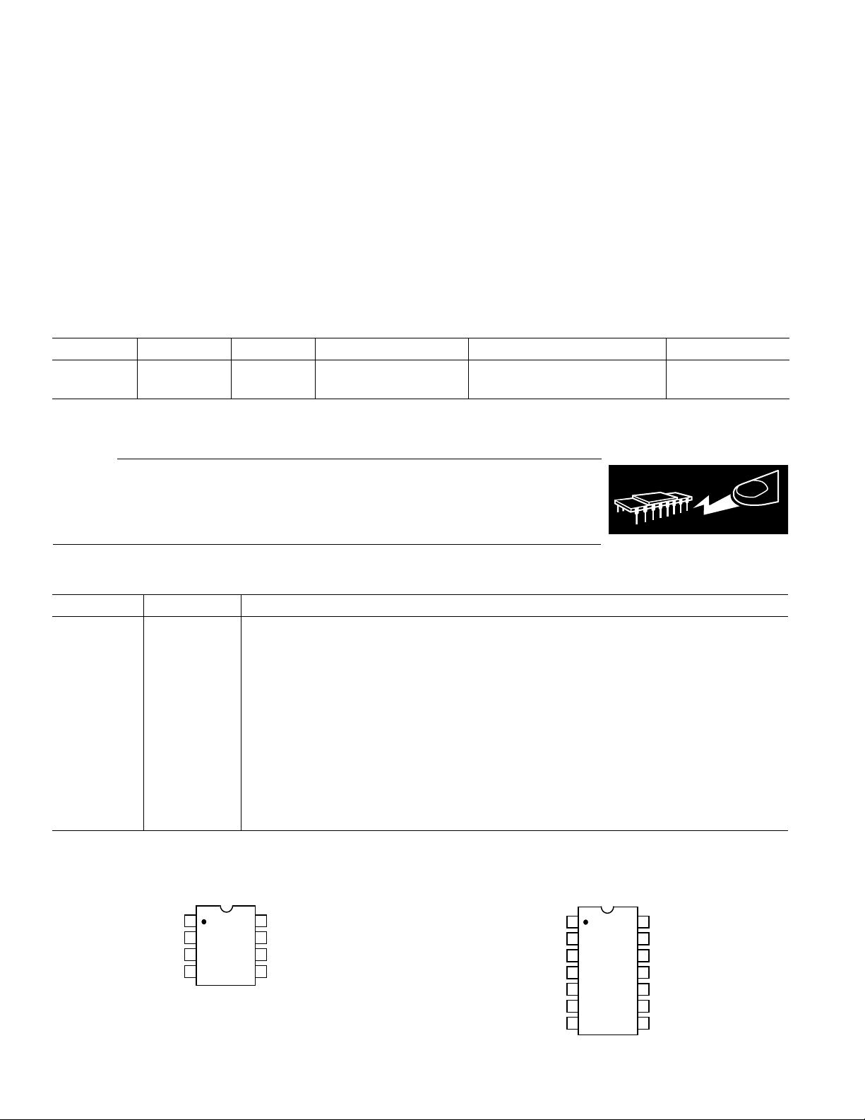
WARNING!
ESD SENSITIVE DEVICE
TOP VIEW
(Not to Scale)
14
13
12
11
10
9
8
1
2
3
4
5
6
7
NC = NO CONNECT
RFB
V
OUT
AGNDF
AGNDS
V
REFS
V
REFF
CS
V
DD
INV
DGND
LDAC
DIN
NC
SCLK
AD5552
ABSOLUTE MAXIMUM RATINGS*
(TA = 25°C unless otherwise noted)
VDD to AGND . . . . . . . . . . . . . . . . . . . . . . . . . –0.3 V to +6 V
Digital Input Voltage to DGND . . . . . –0.3 V to V
V
to AGND . . . . . . . . . . . . . . . . . . –0.3 V to VDD + 0.3 V
OUT
+ 0.3 V
DD
AGND, AGNDF, AGNDS to DGND . . . . . –0.3 V to +0.3 V
Input Current to Any Pin Except Supplies . . . . . . . . ±10 mA
Operating Temperature Range
Industrial (B Version) . . . . . . . . . . . . . . . . –40°C to +85°C
Storage Temperature Range . . . . . . . . . . . . –65°C to +150°C
Maximum Junction Temperature, (T
max) . . . . . . . . . 150°C
J
Package Power Dissipation . . . . . . . . . . . . . (TJ max – TA)/θ
Thermal Impedance θ
JA
JA
SOIC (SO-8) . . . . . . . . . . . . . . . . . . . . . . . . . . 149.5°C/W
SOIC (R-14) . . . . . . . . . . . . . . . . . . . . . . . . . . 104.5°C/W
Lead Temperature, Soldering
Vapor Phase (60 sec) . . . . . . . . . . . . . . . . . . . . . . . . 215°C
Infrared (15 sec) . . . . . . . . . . . . . . . . . . . . . . . . . . . . 220°C
*Stresses above those listed under Absolute Maximum Ratings may cause perma-
nent damage to the device. This is a stress rating only; functional operation of the
device at these or any other conditions above those listed in the operational
sections of this specification is not implied. Exposure to absolute maximum rating
conditions for extended periods may affect device reliability.
ORDERING GUIDE
Model INL DNL Temperature Range Package Description Package Option
AD5551BR ± 1 LSB ± 0.8 LSB –40°C to +85°C 8-Lead Small Outline IC SO-8
AD5552BR ± 1 LSB ± 0.8 LSB –40°C to +85°C 14-Lead Small Outline IC R-14
Die Size = 80 ⫻ 139 = 11,120 sq mil; Number of Transistors = 1230.
CAUTION
ESD (electrostatic discharge) sensitive device. Electrostatic charges as high as 4000 V readily
accumulate on the human body and test equipment and can discharge without detection. Although
the AD5551/AD5552 features proprietary ESD protection circuitry, permanent damage may occur
on devices subjected to high-energy electrostatic discharges. Therefore, proper ESD precautions
are recommended to avoid performance degradation or loss of functionality.
AD5551 PIN FUNCTION DESCRIPTIONS
Mnemonic Pin No. Description
V
OUT
1 Analog Output Voltage from the DAC.
AGND 2 Ground Reference Point for Analog Circuitry.
V
REF
3 This is the voltage reference input for the DAC. Connect to external reference ranges from
2 V to V
DD
.
CS 4 This is an active low-logic input signal. The chip select signal is used to frame the serial
data input.
SCLK 5 Clock Input. Data is clocked into the input register on the rising edge of SCLK. Duty cycle
must be between 40% and 60%.
DIN 6 Serial Data Input. This device accepts 14-bit words. Data is clocked into the input register on
the rising edge of SCLK.
DGND 7 Digital Ground. Ground reference for digital circuitry.
V
DD
8 Analog Supply Voltage, 5 V ± 10%.
AD5551 PIN CONFIGURATION
SOIC
1
V
OUT
2
AGND
V
REF
AD5551
TOP VIEW
3
(Not to Scale)
4
8
7
6
5
V
DD
DGND
DIN
SCLKCS
–4–
AD5552 PIN CONFIGURATION
SOIC
REV. 0
Page 5

AD5551/AD5552
AD5552 PIN FUNCTION DESCRIPTIONS
Mnemonic Pin No. Description
RFB 1 Feedback Resistor. In bipolar mode connect this pin to external op amp output.
V
OUT
AGNDF 3 Ground Reference Point for Analog Circuitry (Force).
AGNDS 4 Ground Reference Point for Analog Circuitry (Sense).
V
REFS
V
REFF
CS 7 This is an active low-logic input signal. The chip select signal is used to frame the serial data input.
SCLK 8 Clock input. Data is clocked into the input register on the rising edge of SCLK. Duty cycle
NC 9 No Connect.
DIN 10 Serial Data Input. This device accepts 14-bit words. Data is clocked into the input register on
LDAC 11 LDAC Input. When this input is taken low, the DAC register is simultaneously updated with
DGND 12 Digital Ground. Ground reference for digital circuitry.
INV 13 Connected to the Internal Scaling Resistors of the DAC. Connect INV pin to external op amps
V
DD
2 Analog Output Voltage from the DAC.
5 This is the voltage reference input (sense) for the DAC. Connect to external reference ranges from
2 V to V
DD
.
6 This is the voltage reference input (force) for the DAC. Connect to external reference ranges
from 2 V to V
DD
.
must be between 40% and 60%.
the rising edge of SCLK.
the contents of the input register.
inverting input in bipolar mode.
14 Analog Supply Voltage, 5 V ± 10%.
TERMINOLOGY
Relative Accuracy
For the DAC, relative accuracy or integral nonlinearity (INL)
is a measure of the maximum deviation, in LSBs, from a straight
line passing through the endpoints of the DAC transfer function.
A typical INL versus code plot can be seen in TPC 1.
Differential Nonlinearity
Differential nonlinearity is the difference between the measured
change and the ideal 1 LSB change between any two adjacent
codes. A specified differential nonlinearity of ±1 LSB maximum
ensures monotonicity. TPC 4 illustrates a typical DNL versus
code plot.
Gain Error
Gain error is the difference between the actual and ideal analog
output range, expressed as a percent of the full-scale range.
It is the deviation in slope of the DAC transfer characteristic
from ideal.
Gain Error Temperature Coefficient
This is a measure of the change in gain error with changes in
temperature. It is expressed in ppm/°C.
Zero Code Error
Zero code error is a measure of the output error when zero code
is loaded to the DAC register.
Zero Code Temperature Coefficient
This is a measure of the change in zero code error with a change
in temperature. It is expressed in mV/°C.
Digital-to-Analog Glitch Impulse
Digital-to-analog glitch impulse is the impulse injected into the
analog output when the input code in the DAC register changes
state. It is normally specified as the area of the glitch in nV-s
and is measured when the digital input code is changed by 1 LSB
at the major carry transition. A plot of the glitch impulse is shown
in TPC 14.
Digital Feedthrough
Digital feedthrough is a measure of the impulse injected into the
analog output of the DAC from the digital inputs of the DAC,
but is measured when the DAC output is not updated. CS is
held high, while the CLK and DIN signals are toggled. It is
specified in nV-s and is measured with a full-scale code change
on the data bus, i.e., from all 0s to all 1s and vice versa. A typical plot of digital feedthrough is shown in TPC 13.
Power Supply Rejection Ratio
This specification indicates how the output of the DAC is affected
by changes in the power supply voltage. Power-supply rejection
ratio is quoted in terms of % change in output per % change in
for full-scale output of the DAC. VDD is varied by ±10%.
V
DD
Reference Feedthrough
This is a measure of the feedthrough from the V
input to the
REF
DAC output when the DAC is loaded with all 0s. A 100 kHz,
1 V p-p is applied to V
. Reference feedthrough is expressed
REF
in mV p-p.
REV. 0
–5–
Page 6

AD5551/AD5552
–Typical Performance Characteristics
0.5
0.25
0
INL – LSB
–0.25
–0.5
0
2048
4096
8192
6144
CODE – Decimal
10240 1433612288
TPC 1. Integral Nonlinearity vs. Code
0.5
0.25
0
INL – LSB
TA = 25ⴗC
V
DD
V
REF
VDD = 5V
V
= 2.5V
REF
= 5V
= 2.5V
16384
0.5
0.25
0
DNL – LSB
–0.25
–0.5
0
2048
4096
8192
6144
CODE – Decimal
10240 1433612288
TPC 4. Differential Nonlinearity vs. Code
0.5
VDD = 5V
V
0.25
0
DNL – LSB
TA = 25ⴗC
V
= 5V
DD
V
= 2.5V
REF
= 2.5V
REF
16384
–0.25
–0.5
–60
–20
TEMPERATURE – ⴗC
6020
100 140
TPC 2. Integral Nonlinearity vs. Temperature
1.0
V
= 2.5V
0.75
0.5
0.25
0
–0.25
LINEARITY ERROR – LSB
–0.5
–0.75
–1.0
23
DNL
54
SUPPLY VOLTAGE – V
REF
T
= 25ⴗC
A
INL
67
TPC 3. Linearity Error vs. Supply Voltage
–0.25
–0.5
–60
–20
TEMPERATURE – ⴗC
6020
100 140
TPC 5. Differential Nonlinearity vs. Temperature
0.25
LINEARITY ERROR – LSB
–0.25
–0.5
0.5
DNL
0
INL
0
23 546
1
REFERENCE VOLTAGE
VDD = 5V
T
= 25ⴗC
A
TPC 6. Linearity Error vs. Reference Voltage
–6–
REV. 0
Page 7

1.00
TEMPERATURE – ⴗC
–50
ZERO-CODE OFFSET ERROR – LSB
0.50
0.25
–25 50
25 100 125
0
0.75
75
150
0
VDD = 5V
V
REF
= 2.5V
CODE – Decimal
0
0
2048
REFERENCE CURRENT – A
50
100
6144
8192
4096
10240 1433612288 16384
150
200
300
250
TA = 25ⴗC
V
DD
= 5V
V
REF
= 2.5V
UNIPOLAR MODE
BIPOLAR MODE
1555H
0155H
2155H
0.75
0.50
0.25
–0.25
GAIN ERROR – LSB
–0.50
–0.75
AD5551/AD5552
VDD = 5V
V
= 2.5V
REF
0
–1.00
–25 50
–50
25
0
TEMPERATURE – ⴗC
75
100 125
TPC 7. Gain Error vs. Temperature
250
VDD = 5V
V
= 5V
LOGIC
V
= 2.5V
REF
A
200
SUPPLY CURRENT –
150
0
–20–40 20 40 60 80 100 120
TEMPERATURE – ⴗC
TPC 8. Supply Current vs. Temperature
400
VDD = 5V
V
= 2.5V
REF
350
T
= 25ⴗC
A
A
300
150
TPC 10. Zero-Code Error vs. Temperature
450
TA = 25ⴗC
400
A
350
300
250
SUPPLY CURRENT –
200
150
REFERENCE
VOLTAGE
= 5V
V
DD
1
3
20456
VOLTAGE – V
SUPPLY
VOLTAGE
= 2.5V
V
REF
TPC 11. Supply Current vs. Reference Voltage or Supply
Voltage
250
SUPPLY CURRENT –
200
150
1
TPC 9. Supply Current vs. Digital Input Voltage
2045
DIGITAL INPUT VOLTAGE – V
3
REV. 0
TPC 12. Reference Current vs. Code
–7–
Page 8

AD5551/AD5552
100
CLOCK (5V/DIV)
90
V
(50mV/DIV)
OUT
10
0%
100
90
CS (5V/DIV)
V
(0.1V/DIV)
OUT
10
0%
V
REF
V
DD
= 25ⴗC
T
A
2s/DIV
TPC 13. Digital Feedthrough
V
V
T
= 2.5V
= 5V
REF
= 5V
DD
= 25ⴗC
A
= 2.5V
2µs/DIV
100
90
10pF
50pF
100pF
10
0%
V
V
T
A
REF
= 5V
DD
= 25ⴗC
200pF
= 2.5V
CS (5V/DIV)
V
(0.5V/DIV)
OUT
TPC 15. Large Signal Settling Time
V
= 2.5V
REF
= 5V
100
90
10
0%
V
DD
T
A
= 25ⴗC
V
(1V/DIV)
OUT
(50mV/DIV)
V
OUT
GAIN = –216
2µs/DIV
TPC 14. Digital-to-Analog Glitch Impulse
GENERAL DESCRIPTION
The AD5551/AD5552 are single, 14-bit, serial input, voltage
output DACs. They operate from a single supply ranging from
2.7 V to 5 V and consume typically 300 A with a supply of
5 V. Data is written to these devices in a 14-bit word format, via
a 3- or 4-wire serial interface. To ensure a known power-up state,
these parts were designed with a power-on reset function. In unipolar mode, the output is reset to 0 V, while in bipolar mode, the
AD5552 output is set to –V
. Kelvin sense connections for
REF
the reference and analog ground are included on the AD5552.
Digital-to-Analog Section
The DAC architecture consists of two matched DAC sections.
A simplified circuit diagram is shown in Figure 2. The DAC
architecture of the AD5551/AD5552 is segmented. The four
MSBs of the 14-bit data word are decoded to drive 15 switches,
E1 to E15. Each of these switches connects one of 15 matched
resistors to either AGND or V
. The remaining 10 bits of the
REF
data word drive switches S0 to S9 of a 10-bit voltage mode
R-2R ladder network.
2R 2R 2R
V
REF
R
S0 S1
10-BIT R-2R LADDER
R
2R 2R 2R 2R
S9
E1 E2 E15
FOUR MSBs DECODED INTO
15 EQUAL SEGMENTS
V
OUT
Figure 2. DAC Architecture
0.5s/DIV
TPC 16. Small Signal Settling Time
With this type of DAC configuration, the output impedance
is independent of code, while the input impedance seen by the reference is heavily code dependent. The output voltage is dependent
on the reference voltage as shown in the following equation.
VD
×
V
OUT
REF
=
N
2
where D is the decimal data word loaded to the DAC register
and N is the resolution of the DAC. For a reference of 2.5 V,
the equation simplifies to the following.
D
×25
=
16 384.,
giving a V
V
OUT
of 1.25 V with midscale loaded, and 2.5 V with
OUT
full-scale loaded to the DAC.
The LSB size is V
/16,384.
REF
Serial Interface
The AD5551 and AD5552 are controlled by a versatile 3-wire
serial interface, which operates at clock rates up to 25 MHz and
is compatible with SPI, QSPI, MICROWIRE, and DSP interface
standards. The timing diagram can be seen in Figure 1. Input
data is framed by the chip select input, CS. After a high-to-low
transition on CS, data is shifted synchronously and latched into
the input register on the rising edge of the serial clock, SCLK.
Data is loaded MSB first in 14-bit words. After 14 data bits
have been loaded into the serial input register, a low-to-high
transition on CS transfers the contents of the shift register to the
DAC. Data can only be loaded to the part while CS is low.
–8–
REV. 0
Page 9

The AD5552 has an LDAC function that allows the DAC latch
AD5551/AD5552
DGND
V
DD
V
REFS
V
REFF
OUT
SCLK
DIN
CS
5V
2.5V
EXTERNAL
OP AMP
BIPOLAR
OUTPUT
10F
SERIAL
INTERFACE
0.1F
LDAC
0.1F
INV
R
INV
+5V
–5V
R
FB
RFB
AGNDSAGNDF
V
VVRDVRD
RD A
OUT BIP
OUT UNI OS REF
–
–
–
/
=
+
()
+
()
+
()
[]
++
()
21
12
to be updated asynchronously by bringing LDAC low after CS
goes high. LDAC should be maintained high while data is written
to the shift register. Alternatively, LDAC may be tied permanently
low to update the DAC synchronously. With LDAC tied perma-
nently low, the rising edge of CS will load the data to the DAC.
Unipolar Output Operation
These DACs are capable of driving unbuffered loads of 60 kΩ.
Unbuffered operation results in low-supply current, typically
300 µA, and a low-offset error. The AD5551 provides a unipolar
output swing ranging from 0 V to V
. The AD5552 can be
REF
configured to output both unipolar and bipolar voltages. Figure 3 shows a typical unipolar output voltage circuit. The code
table for this mode of operation is shown in Table I.
AD5551/AD5552
Figure 4. Bipolar Output (AD5552 Only)
Table II. Bipolar Code Table
SERIAL
INTERFACE
*
AD5552 ONLY
0.1F
5V 2.5V
V
V
DD
CS
DIN
SCLK
LDAC
REFF
AD5551/AD5552
*
DGND
0.1F
*
10F
V
AGND
REFS
*
AD820/
OUT
OP196
EXTERNAL
OP AMP
UNIPOLAR
OUTPUT
DAC Latch Contents
MSB LSB Analog Output
11 1111 1111 1111 +V
10 0000 0000 0000 +V
× (8191/8192)
REF
× (1/8192)
REF
00 0000 0000 0001 0 V
00 0000 0000 0000 –V
00 0000 0000 0000 –V
× (1/8192)
REF
× (8191/8192) = –V
REF
REF
Assuming a perfect reference, the worst-case bipolar output
voltage may be calculated from the following equation.
Bipolar Mode Worst-Case Output
Figure 3. Unipolar Output
Table I. Unipolar Code Table
DAC Latch Contents
MSB LSB Analog Output
11 1111 1111 1111 V
10 0000 0000 0000 V
00 0000 0000 0001 V
× (16383/16384)
REF
× (8192/16384) = 1/2 V
REF
× (1/16384)
REF
REF
00 0000 0000 0000 0 V
Assuming a perfect reference, the worst-case output voltage may
be calculated from the following equation.
Unipolar Mode Worst-Case Output
V
OUT UNI REF GE ZSE–
D
V V V INL
()=× + + +
14
2
where
V
OUT–UNI
= Unipolar Mode Worst-Case Output
D = Decimal Code Loaded to DAC
V
REF
V
GE
V
ZSE
= Reference Voltage Applied to Part
= Gain Error in Volts
= Zero Scale Error in Volts
INL = Integral Nonlinearity in Volts
Bipolar Output Operation
With the aid of an external op amp, the AD5552 may be configured to provide a bipolar voltage output. A typical circuit of
such operation is shown in Figure 4. The matched bipolar offset
resistors R
achieve this bipolar output swing where R
Table II shows the transfer function for this output operating
mode. Also provided on the AD5552 are a set of Kelvin connections to the analog ground inputs.
REV. 0
and R
FB
are connected to an external op amp to
INV
= R
FB
INV
= 28 kΩ.
where
V
= External Op Amp Input Offset Voltage
OS
RD = RFB and RIN Resistor Matching Error, Unitless
A = Op Amp Open-Loop Gain
Output Amplifier Selection
For bipolar mode, a precision amplifier should be used, supplied
from a dual power supply. This will provide the ±V
output.
REF
In a single-supply application, selection of a suitable op amp
may be more difficult as the output swing of the amplifier does
not usually include the negative rail, in this case AGND. This
can result in some degradation of the specified performance
unless the application does not use codes near zero.
The selected op amp needs to have very low-offset voltage, (the
DAC LSB is 152 µV with a 2.5 V reference), to eliminate the
need for output offset trims. Input bias current should also be
very low as the bias current multiplied by the DAC output
impedance (approximately 6K) will add to the zero code error.
Rail-to-rail input and output performance is required. For fast
settling, the slew rate of the op amp should not impede the
settling time of the DAC. Output impedance of the DAC is
constant and code-independent, but in order to minimize gain
errors, the input impedance of the output amplifier should be
as high as possible. The amplifier should also have a 3 dB bandwidth of 1 MHz or greater. The amplifier adds another time
constant to the system, hence increasing the settling time of the
output. A higher 3 dB amplifier bandwidth results in a faster
effective settling time of the combined DAC and amplifier.
–9–
Page 10

AD5551/AD5552
Force Sense Buffer Amplifier Selection
These amplifiers can be single-supply or dual supplies, lownoise amplifiers. A low-output impedance at high frequencies
is preferred as they need to be able to handle dynamic currents
of up to ± 20 mA.
Reference and Ground
As the input impedance is code-dependent, the reference pin
should be driven from a low-impedance source. The AD5551/
AD5552 operates with a voltage reference ranging from 2 V to
. Although DAC’s full-scale output voltage is determined
V
DD
by the reference, references below 2 V will result in reduced
accuracy. Tables I and II outline the analog output voltage
for particular digital codes. For optimum performance, Kelvin
sense connections are provided on the AD5552.
If the application does not require separate force and sense lines,
they should be tied together close to the package to minimize
voltage drops between the package leads and the internal die.
ADR291 and ADR293 are suitable references for this product.
Power-On Reset
These parts have a power-on reset function to ensure the output
is at a known state upon power-up. On power-up, the DAC
register contains all zeros, until data is loaded from the serial
register. However, the serial register is not cleared on power-up,
so its contents are undefined. When loading data initially to the
DAC, 14 bits or more should be loaded to prevent erroneous
data appearing on the output. If more than 14 bits are loaded,
only the last 14 are kept, and if fewer than 14 are loaded, bits
will remain from the previous word. If the AD5551/AD5552
needs to be interfaced with data shorter than 14 bits, the data
should be padded with zeros at the LSBs.
Power Supply and Reference Bypassing
For accurate high-resolution performance, it is recommended that
the reference and supply pins be bypassed with a 10 µF tantalum
capacitor in parallel with a 0.1 µF ceramic capacitor.
**
FO
ADSP-2101/
ADSP-2103
*
ADDITIONAL PINS OMITTED FOR CLARITY.
**
AD5552 ONLY
*
TFS
DT
SCLK
LDAC
CS
DIN
SCLK
AD5551/
AD5552
*
Figure 5. ADSP-2101/ADSP-2103 to AD5551/AD5552
Interface
68HC11 to AD5551/AD5552 Interface
Figure 6 shows a serial interface between the AD5551/AD5552
and the 68HC11 microcontroller. SCK of the 68HC11 drives
the SCLK of the DAC, while the MOSI output drives the
serial data lines SDIN. CS signal is driven from one of the
port lines. The 68HC11 is configured for master mode; MSTR
= 1, CPOL = 0, and CPHA = 0. Data appearing on the MOSI
output is valid on the rising edge of SCK.
**
PC6
68HC11/
68L11
*
ADDITIONAL PINS OMITTED FOR CLARITY.
**
AD5552 ONLY
PC7
*
MOSI
SCK
LDAC
CS
DIN
SCLK
AD5551/
AD5552
*
Figure 6. 68HC11/68L11 to AD5551/AD5552 Interface
MICROWIRE to AD5551/AD5552 Interface
Figure 7 shows an interface between the AD5551/AD5552 and
any MICROWIRE-compatible device. Serial data is shifted out
on the falling edge of the serial clock and into the AD5551/
AD5552 on the rising edge of the serial clock. No glue logic is
required as the DAC clocks data into the input shift register on
the rising edge.
MICROPROCESSOR INTERFACING
Microprocessor interfacing to the AD5551/AD5552 is via a
serial bus that uses standard protocol compatible with DSP
processors and microcontrollers. The communications channel
requires a 3-wire interface consisting of a clock signal, a data
signal and a synchronization signal. The AD5551/AD5552
requires a 14-bit data word with data valid on the rising edge of
SCLK. The DAC update may be done automatically when all
the data is clocked in or it may be done under control of LDAC
(AD5552 only).
ADSP-2101/ADSP-2103 to AD5551/AD5552 Interface
Figure 5 shows a serial interface between the AD5551/AD5552
and the ADSP-2101/ADSP-2103. The ADSP-2101/ADSP-2103
should be set to operate in the SPORT (Serial Port) transmit
alternate framing mode. The ADSP-2101/ADSP-2103 is programmed through the SPORT control register and should be
configured as follows: Internal Clock Operation, Active Low
Framing, 16-Bit Word Length. The first 2 bits are DON’T CARE
as AD5551/AD5552 will keep the last 14 bits. Transmission is
initiated by writing a word to the Tx register after the SPORT has
been enabled. Because of the edges-triggered difference, an inverter
is required at the SCLKs between the DSP and the DAC.
CS
MICROWIRE
*
ADDITIONAL PINS OMITTED FOR CLARITY.
*
SCLK
SO
CS
DIN
SCLK
AD5551/
AD5552
*
Figure 7. MICROWIRE to AD5551/AD5552 Interface
80C51/80L51 to AD5551/AD5552 Interface
A serial interface between the AD5551/AD5552 and the 80C51/
80L51 microcontroller is shown in Figure 8. TxD of the
microcontroller drives the SCLK of the AD5551/AD5552, while
RxD drives the serial data line of the DAC. P3.3 is a bit programmable pin on the serial port which is used to drive CS.
P3.4
80C51/
80L51
*
ADDITIONAL PINS OMITTED FOR CLARITY.
**
AD5552 ONLY
P3.3
*
RxD
TxD
LDAC
CS
DIN
SCLK
**
AD5551/
AD5552
*
Figure 8. 80C51/80L51 to AD5551/AD5552 Interface
–10–
REV. 0
Page 11

AD5551/AD5552
ENABLE
DIN
SCLK
DGND
CODED
ADDRESS
DECODER
V
DD
EN
AD5551/AD5552
CS
DIN
SCLK
V
OUT
AD5551/AD5552
CS
DIN
SCLK
V
OUT
AD5551/AD5552
CS
DIN
SCLK
V
OUT
AD5551/AD5552
CS
DIN
SCLK
V
OUT
The 80C51/80L51 provides the LSB first, while the AD5551/
AD5552 expects the MSB of the 14-bit word first. Care should be
taken to ensure the transmit routine takes this into account.
Usually it can be done through software by shifting out and accumulating the bits in the correct order before inputting to the DAC.
Also, 80C51 outputs 2 byte words/16 bits data, thus the first two
bits, after rearrangement, should be DON’T CARE as they will
be dropped from the DAC’s 14-bit word.
When data is to be transmitted to the DAC, P3.3 is taken low.
Data on RxD is valid on the falling edge of TxD, so the clock must
be inverted as the DAC clocks data into the input shift register on
the rising edge of the serial clock. The 80C51/80L51 transmits
its data in 8-bit bytes with only eight falling clock edges occurring in the transmit cycle. As the DAC requires a 14-bit word,
P3.3 (or any one of the other programmable bits) is the CS input
signal to the DAC, so P3.3 should be brought low at the beginning of the 16-bit write cycle 2 × 8 bit words and held low until
the 16-bit 2 × 8 cycle is completed. After that, P3.3 is brought
high again and the new data loads to the DAC. Again, the first
two bits, after rearranging, should be DON’T CARE. LDAC
on the AD5552 may also be controlled by the 80C51/80L51 serial
port output by using another bit programmable pin, P3.4.
APPLICATIONS
Optocoupler interface
The digital inputs of the AD5551/AD5552 are Schmitttriggered, so they can accept slow transitions on the digital input
lines. This makes these parts ideal for industrial applications
where it may be necessary that the DAC is isolated from the
controller via optocouplers. Figure 9 illustrates such an interface.
Decoding Multiple AD5551/AD5552s
The CS pin of the AD5551/AD5552 can be used to select one
of a number of DACs. All devices receive the same serial clock
and serial data, but only one device will receive the CS signal at
any one time. The DAC addressed will be determined by the
decoder. There will be some digital feedthrough from the digital
input lines. Using a burst clock will minimize the effects of digital feedthrough on the analog signal channels. Figure 10 shows a
typical circuit.
5V
V
10k⍀
V
10k⍀
V
10k⍀
REGULATOR
DD
SCLK
DD
AD5551/AD5552
CS
DD
DIN
V
GND
POWER
SCLK
CS
DIN
Figure 9. AD5551/AD5552 in an Optocoupler Interface
10F
DD
V
OUT
Figure 10. Addressing Multiple AD5551/AD5552s
0.1F
REV. 0
–11–
Page 12

AD5551/AD5552
OUTLINE DIMENSIONS
Dimensions shown in inches and (mm).
0.1574 (4.00)
0.1497 (3.80)
PIN 1
0.0098 (0.25)
0.0040 (0.10)
SEATING
0.1968 (5.00)
0.1890 (4.80)
85
0.0500 (1.27)
BSC
PLANE
0.2440 (6.20)
0.2284 (5.80)
41
0.0192 (0.49)
0.0138 (0.35)
8-Lead SO
(SO-8)
0.0688 (1.75)
0.0532 (1.35)
0.0098 (0.25)
0.0075 (0.19)
0.0196 (0.50)
0.0099 (0.25)
8ⴗ
0.0500 (1.27)
0ⴗ
0.0160 (0.41)
ⴛ 45ⴗ
0.1574 (4.00)
0.1497 (3.80)
PIN 1
0.0098 (0.25)
0.0040 (0.10)
0.3444 (8.75)
0.3367 (8.55)
14
1
0.050 (1.27)
BSC
8
7
0.0688 (1.75)
0.0532 (1.35)
0.0192 (0.49)
0.0138 (0.35)
14-Lead SO
(R-14)
0.2440 (6.20)
0.2284 (5.80)
SEATING
0.0099 (0.25)
PLANE
0.0075 (0.19)
0.0196 (0.50)
0.0099 (0.25)
8ⴗ
0ⴗ
0.0500 (1.27)
0.0160 (0.41)
ⴛ 45ⴗ
C01943–5–7/00 (rev. 0)
–12–
PRINTED IN U.S.A.
REV. 0
 Loading...