

Page 1
Dual Current Output, Parallel Input, 16-/14-Bit
V
(
(
Multiplying DACs with 4-Quadrant Resistors
FEATURES
Dual channel
16-bit resolution: AD5547
14-bit resolution: AD5557
2- or 4-quadrant, 4 MHz BW multiplying DAC
±1 LSB DNL
±1 LSB INL for AD5557, ±2 LSB INL for AD5547
Operating supply voltage: 2.7 V to 5.5 V
Low noise: 12 nV/√
Low power: I
DD
0.5 µs settling time
Built-in R
facilitates current-to-voltage conversion
FB
Built-in 4-quadrant resistors allow 0 V to –10 V, 0 V to +10 V,
or ±10 V outputs
2 mA full-scale current ± 20%, with V
Extended automotive operating temperature range:
–40°C to +125°C
Selectable zero-scale/midscale power-on presets
Compact TSSOP-38 package
APPLICATIONS
Automatic test equipment
Instrumentation
Digitally controlled calibration
Digital waveform generation
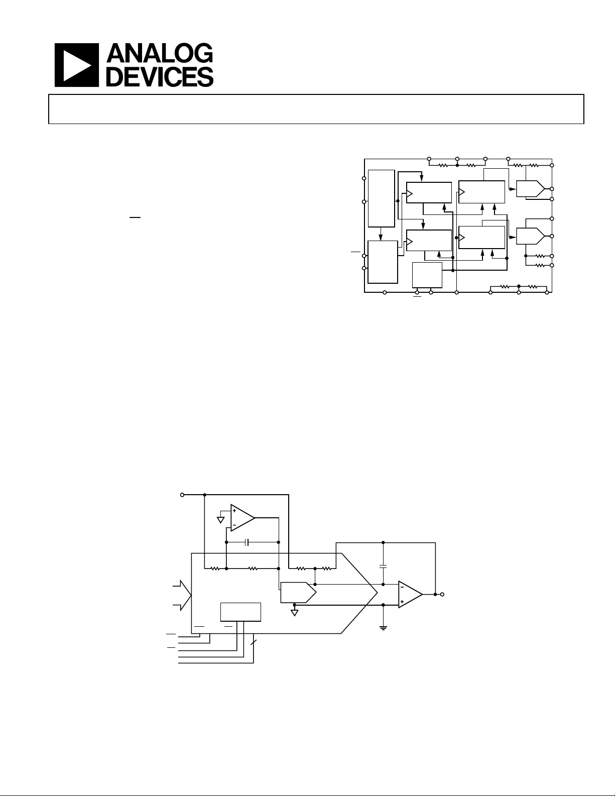
GENERAL DESCRIPTION
The AD5547/AD5557 are dual precision, 16-/14-bit,
multiplying, low power, current-output, parallel input, digitalto-analog converters. They are designed to operate from single
+5 V supply with ±10 V multiplying references for 4-quadrant
outputs with up to 4 MHz bandwidth.
Hz
= 10 µA max
VREF
= 10 V
REF
U1
–VREF
AD5547/AD5557
FUNCTIONAL BLOCK DIAGRAM
R
R
COMA
1A
V
D0–D15
AD5547)
D0–D13
AD5557)
WR
A0, A1
DD
D0..D15
OR
D0..D13
DAC A
DAC B
ADDR
DECODE
INPUT
REGISTER
INPUT
REGISTER
POWER
ON
RESET
MSB LDACDGND
RS
REGISTER
RS
REGISTER
RS
AD5547/AD5557
Figure 1.
The built-in 4-quadrant resistors facilitate resistance matching
and temperature tracking, which minimize the numbers of
components needed for multiquadrant applications. In addition,
the feedback resistor (R
) simplifies the I-V conversion with an
FB
external buffer.
The AD5547/AD5557 are available in a compact TSSOP-38
package and operate at the extended automotive temperature
range of –40°C to +125°C.
REFA
DAC A
DAC B
R
OFSA
R
FBA
V
REFB
I
OUTA
AGNDA
AGNDB
I
OUTB
R
FBB
R
OFSB
04452-0-013
DAC A
RS
DAC B
RS
R
R
COMB
1B
C1
R
COMA
RESET
V
MSB A0, A1
2
R
REFA
OFSARFBA
16-/14-BIT
DAC A
(ONE CHANNEL SHOWN ONLY)
IOUTA
C2
U2
VOUTA
–VREF TO +VREF
04452-0-002
RFBROFS
AGNDA
16/14 DATA
WR
LDAC
RS
MSB
A0, A1
R
1A
R1 R2
AD5547/AD5557
POWER-ON
WR RSLDAC
Figure 2. 16/14-Bit 4-Quadrant Multiplying DAC with Minimum of External Components (Only One Channel Shown)
Rev. 0
Information furnished by Analog Devices is believed to be accurate and reliable.
However, no responsibility is assumed by Analog Devices for its use, nor for any
infringements of patents or other rights of third parties that may result from its use.
Specifications subject to change without notice. No license is granted by implication
or otherwise under any patent or patent rights of Analog Devices. Trademarks and
registered trademarks are the property of their respective owners.
One Technology Way, P.O. Box 9106, Norwood, MA 02062-9106, U.S.A.
Tel: 781.329.4700
Fax: 781.326.8703 © 2004 Analog Devices, Inc. All rights reserved.
www.analog.com
Page 2

AD5547/AD5557
TABLE OF CONTENTS
Specifications..................................................................................... 3
Absolute Maximum Ratings............................................................ 5
ESD Caution.................................................................................. 5
Pin Configurations and Function Descriptions ........................... 6
Typical Performance Characteristics ............................................. 9
Circuit Operation ...........................................................................12
D/A Converter Section .............................................................. 12
Digital Section............................................................................. 13
REVISION HISTORY
Revision 0: Initial Version
PCB Layout, Power Supply Bypassing, and Ground
Connections ................................................................................ 13
Applications..................................................................................... 14
Unipolar Mode ........................................................................... 14
Bipolar Mode .............................................................................. 16
Outline Dimensions....................................................................... 19
Ordering Guide .......................................................................... 19
Rev. 0 | Page 2 of 20
Page 3

AD5547/AD5557
SPECIFICATIONS
VDD = 2.7 V to 5.5 V, I
Table 1. Electrical Characteristics
Parameter Symbol Conditions Min Typ Max Unit
STATIC PERFORMANCE1
Resolution N AD5547, 1 LSB = V
AD5557, 1 LSB = V
Relative Accuracy INL Grade: AD5557C ±1 LSB
Grade: AD5547B ±2 LSB
Differential Nonlinearity DNL Monotonic ±1 LSB
Output Leakage Current I
Data = zero scale, TA = TA maximum 20 nA
Full-Scale Gain Error G
Bipolar Mode Gain Error GE Data = full scale ±1 ±4 mV
Bipolar Mode Zero-Scale Error G
Full-Scale Tempco2 TCVFS 1 ppm/°C
REFERENCE INPUT
V
Range V
REF
REF Input Resistance REF 4 5 6 kΩ
R1 and R2 Resistance R1 and R2 4 5 6 kΩ
R1-to-R2 Mismatch ∆(R1 to R2) ±0.5 ±1.5 Ω
Feedback and Offset Resistance RFB, R
Input Capacitance2 C
ANALOG OUTPUT
Output Current I
Output Capacitance2 C
LOGIC INPUT AND OUTPUT
Logic Input Low Voltage VIL V
V
Logic Input High Voltage VIH V
V
Input Leakage Current IIL 10 µA
Input Capacitance2 C
INTERFACE TIMING
Data to WR Setup Time
V
Data to WR Hold Time
V
WR Pulse Width
V
LDAC Pulse Width t
V
RS Pulse Width
V
WR to LDAC Delay Time
V
SUPPLY CHARACTERISTICS
Power Supply Range V
Positive Supply Current IDD Logic inputs = 0 V 10 µA
Power Dissipation P
Power Supply Sensitivity PSS ∆VDD = ±5% 0.003 %/%
= Virtual GND, GND = 0 V, V
OUT
Data = zero scale, TA = 25°C 10 nA
OUT
Data = full scale ±1 ±4 mV
FSE
Data = full scale ±1 ±3 mV
ZSE
–18 +18 V
REF
8 10 12 kΩ
OFS
5 pF
REF
Data = full scale 2 mA
OUT
Code dependent 200 pF
OUT
10 pF
2, 3
IL
t
V
DS
t
V
DH
t
WR
V
LDAC
t
V
RS
t
V
LWD
2.7 5.5 V
DD RANGE
Logic inputs = 0 V 0.055 mW
DISS
= –10 V to +10 V, TA = –40°C to +125°C, unless otherwise noted.
REF
/216 = 153 µV at V
REF
/214 = 610 µV at V
REF
= 5 V 0.8 V
DD
= 3 V 0.4 V
DD
= 5 V 2.4 V
DD
= 3 V 2.1 V
DD
= 5 V 20 ns
DD
= 3 V 35 ns
DD
= 5 V 0 ns
DD
= 3 V 0 ns
DD
= 10 V 16 Bits
REF
= 10 V 14 Bits
REF
VDD = 5 V 20 ns
= 3 V 35 ns
DD
= 5 V 20 ns
DD
= 3 V 35 ns
DD
= 5 V 20 ns
DD
= 3 V 35 ns
DD
= 5 V 0 ns
DD
= 3 V 0 ns
DD
Rev. 0 | Page 3 of 20
Page 4
AD5547/AD5557
Parameter Symbol Conditions Min Typ Max Unit
AC CHARACTERISTICS4
Output Voltage Settling Time tS
To ±0.1% of full scale, data cycles from zero scale
to full scale to zero scale
Reference Multiplying BW BW V
DAC Glitch Impulse Q V
Multiplying Feedthrough Error V
OUT/VREF
V
Digital Feedthrough QD
Total Harmonic Distortion THD V
= 5 V p-p, data = full scale 4 MHz
REF
= 0 V, midscale to midscale – 1 7 nV-s
REF
= 100 mV rms, f = 10 kHz –65 dB
REF
WR = 1, LDAC toggles at 1 MHz
= 5 V p-p, data = full scale, f = 1 kHz –85 dB
REF
Output Noise Density eN f = 1 kHz, BW = 1 Hz 12
Analog Crosstalk CAT
Signal input at Channel A and measure the output
at Channel B, f = 1 kHz
1
All static performance tests (except I
to the amplifier output. The OP97’s +IN pin is grounded, and the DAC’s I
2
Guaranteed by design; not subject to production testing.
3
All input control signals are specified with tR = tF = 2.5 ns (10% to 90% of 3 V), and are timed from a voltage level of 1.5 V.
4
All ac characteristic tests are performed in a closed-loop system using an AD841 I-V converter amplifier.
) are performed in a closed-loop system using an external precision OP97 I-V converter amplifier. The device RFB terminal is tied
OUT
is tied to the OP97’s –IN pin. Typical values represent average readings measured at 25°C.
OUT
t
WR
WR
0.5 µs
7 nV-s
Hz
nV/√
–95 dB
DATA
t
DH
t
LWD
t
LDAC
t
RS
03810-0-005
LDAC
RS
t
DS
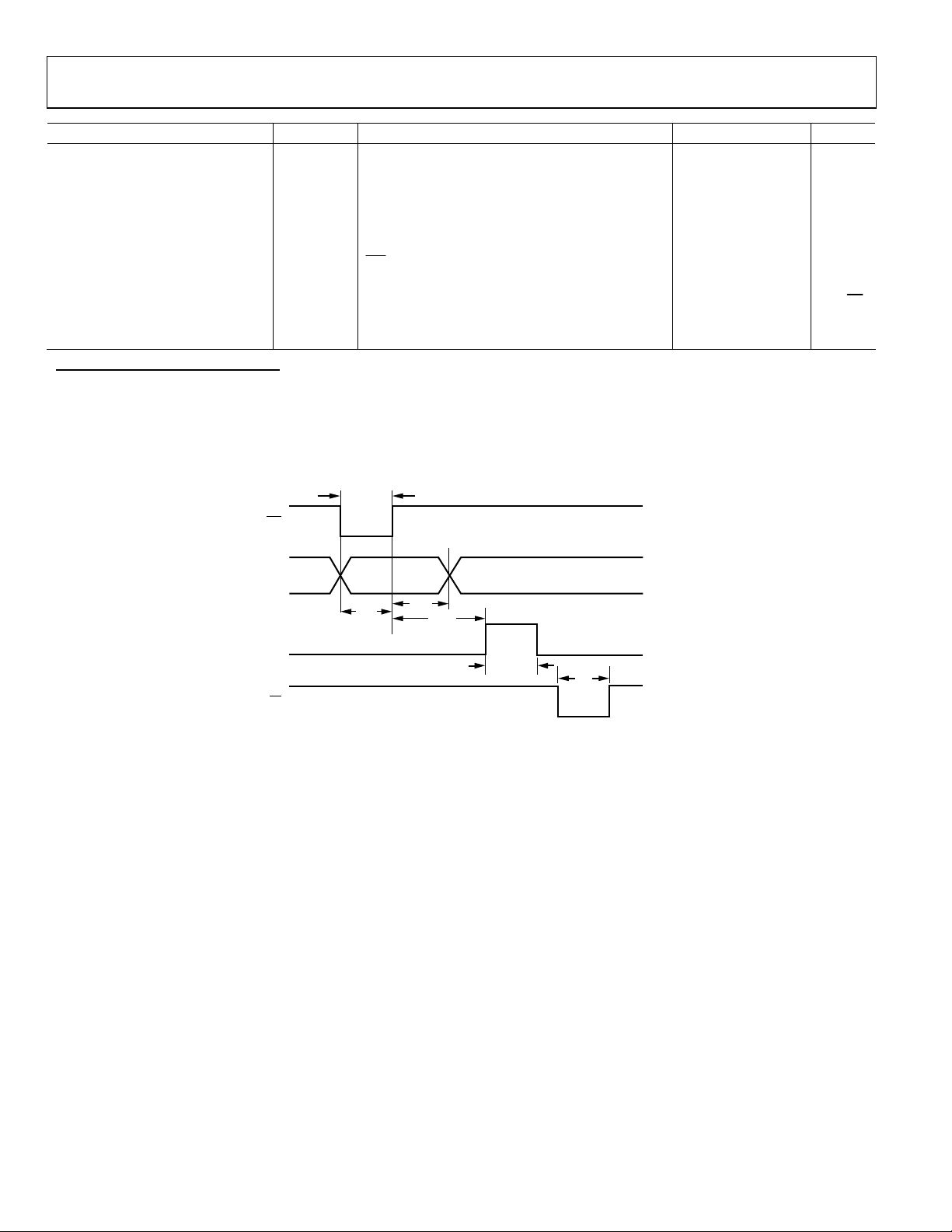
Figure 3. AD5547/AD5557 Timing Diagram
Rev. 0 | Page 4 of 20
Page 5

AD5547/AD5557
ABSOLUTE MAXIMUM RATINGS
Table 2.
Parameter Rating
VDD to GND –0.3 V, +8 V
RFB, R
OFS
, R1, R
, and VREF to GND –18 V, 18 V
COM
Logic Inputs to GND –0.3 V, +8 V
V(I
) to GND –0.3 V, VDD + 0.3 V
OUT
Input Current to Any Pin except Supplies ±50 mA
Thermal Resistance (θJA)1
Maximum Junction Temperature (TJ
) 150°C
MAX
Operating Temperature Range –40°C to +125°C
Storage Temperature Range –65°C to +150°C
Lead Temperature
Vapor Phase, 60 s 215°C
Infrared, 15 s 220°C
Stresses above those listed under Absolute Maximum Ratings
may cause permanent damage to the device. This is a stress
rating only; functional operation of the device at these or any
other conditions above those listed in the operational sections
of this specification is not implied. Exposure to absolute
maximum rating conditions for extended periods may affect
device reliability.
1
Package power dissipation = (T
J MAX
– TA)/θJA.
ESD CAUTION
ESD (electrostatic discharge) sensitive device. Electrostatic charges as high as 4000 V readily accumulate on
the human body and test equipment and can discharge without detection. Although this product features
proprietary ESD protection circuitry, permanent damage may occur on devices subjected to high energy
electrostatic discharges. Therefore, proper ESD precautions are recommended to avoid performance
degradation or loss of functionality.
Rev. 0 | Page 5 of 20
Page 6
AD5547/AD5557
A
A
A
A
A
A
A
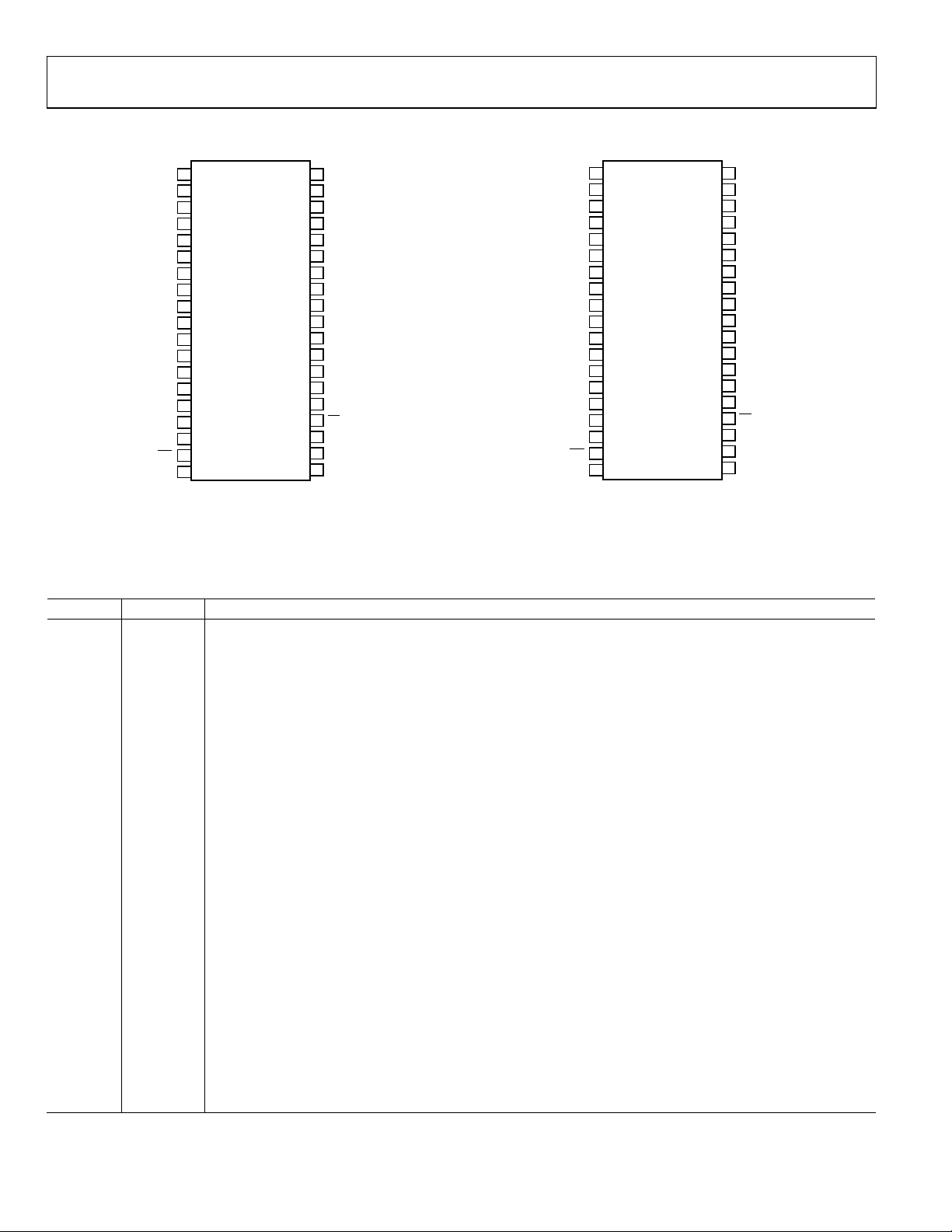
PIN CONFIGURATIONS AND FUNCTION DESCRIPTIONS
R
OFSA
R
R
COMA
V
REFA
I
OUTA
GND
DGND
GND
I
OUTB
V
REFB
R
COMB
R
R
OFSB
FBA
R
R
FBB
WR
1
D1
2
D0
3
4
5
1A
6
7
8
AD5547
9
10
11
12
13
14
15
1B
16
17
18
19
A0
TOP VIEW
(Not to Scale)
38
D2
D3
37
D4
36
D5
35
34
D6
33
D7
D8
32
D9
31
D10
30
29
VDD
28
D11
D12
27
D13
26
D14
25
24
D15
23
RS
MSB
22
LDAC
21
A1
20
Figure 4. AD5547 TSSOP-38 Pin Configuration
Table 3. AD5547 Pin Function Descriptions
Pin No. Mnemonic Function
1, 2, 24–
D0–D15 Digital Input Data Bits D0 to D15. Signal level must be ≤ V
28, 30–38
3 R
4 R
5 R1A
OFSA
Internal Matching Feedback Resistor A. Connects to the external op amp for I-V conversion.
FBA
Bipolar Offset Resistor A. Accepts up to ±18 V. In 2-quadrant mode, R
ties to R
and the external reference.
1A
4-Quandrant Resistor. In 2-quadrant mode, R
not connect when operating in unipolar mode.
6 R
COMA
Center Tap Point of the Two 4-Quadrant Resistors, R
node of the reference amplifier. In 2-quadrant mode, R
unipolar mode.
7 V
REFA
DAC A Reference Input in 2-Quadrant Mode, R2 Terminal in 4-Quadrant Mode. In 2-quadrant mode, V
reference input with constant input resistance versus code. In 4-quadrant mode, V
reference amplifier.
8 I
DAC A Current Output. Connects to the inverting terminal of external precision I-V op amp for voltage output.
OUTA
9 AGNDA DAC A Analog Ground.
10 DGND Digital Ground.
11 AGNDB DAC B Analog Ground.
12 I
13 V
DAC B Current Output. Connects to inverting terminal of external precision I-V op amp for voltage output.
OUTB
REFB
DAC B Reference Input Pin. Establishes DAC full-scale voltage. Constant input resistance versus code. If
configured with an external op amp for 4-quadrant multiplying, V
14 R
COMB
Center Tap Point of the Two 4-Quadrant Resistors, R
node of the reference amplifier. In 2-quadrant mode, R
unipolar mode.
15 R1B
4-Quandrant Resistor. In 2-quadrant mode, R
connect if operating in unipolar mode.
16 R
17 R
Internal Matching Feedback Resistor B. Connects to external op amp for I-V conversion.
FBB
OFSB
Bipolar Offset Resistor B. Accepts up to ±18 V. In 2-quadrant mode, R
ties to R
and an external reference.
1B
04452-0-003
shorts to the V
1A
1A
1B
shorts to the V
1B
R
OFSA
R
R
COMA
V
REFA
I
OUTA
GND
DGND
GNDB
I
OUTB
V
REFB
R
COMB
R
R
OFSB
NC
NC
FBA
R
R
FBB
WR
1
2
3
4
5
1A
6
7
8
AD5557
9
10
11
12
13
14
15
1B
16
17
18
19
A0
TOP VIEW
(Not to Scale)
NC = NO CONNECT
38
D0
D1
37
36
D2
D3
35
34
D4
D5
33
32
D6
D7
31
D8
30
VDD
29
D9
28
D10
27
D11
26
25
D12
D13
24
23
RS
MSB
22
21
LDAC
A1
20
04452-0-004
Figure 5. AD5557 TSSOP-38 Pin Configuration
+ 0.3 V.
DD
ties to R
OFSA
pin. In 4-quadrant mode, R1A ties to R
REFA
and R2A. In 4-quadrant mode, R
shorts to the VREF pin. Do not connect if operating in
COMA
becomes –V
REFB
and R2B. In 4-quadrant mode, R
shorts to the VREF pin. Do not connect if operating in
COMB
pin. In 4-quadrant mode, R1B ties to R
REFB
ties to R
OFSB
. In 4-quadrant mode, R
FBA
ties to the inverting
COMA
is driven by the external
REFA
.
REF
ties to the inverting
COMB
. In 4-quadrant mode, R
FBB
OFSA
REFA
OFSB
OFSA
. Do
is the
. Do not
OFSB
Rev. 0 | Page 6 of 20
Page 7

AD5547/AD5557
Pin No. Mnemonic Function
18
19 A0 Address Pin 0. Signal level must be ≤ V
20 A1 Address Pin 1. Signal level must be ≤ V
21 LDAC Digital Input Load DAC Control. Signal level must be ≤ VDD + 0.3 V.
22 MSB
23
29 VDD Positive Power Supply Input. The specified range of operation is 2.7 V to 5.5 V.
Table 4. AD5557 Pin Function Descriptions
Pin No. Mnemonic Function
1, 2 NC No Connection. Do not connect anything other than dummy pads to these pins.
3 R
4 R
5 R1A
6 R
7 V
8 I
9 AGNDA DAC A Analog Ground.
10 DGND Digital Ground.
11 AGNDB DAC B Analog Ground.
12 I
13 V
14 R
15 R1B
16 R
17 R
18
19 A0 Address Pin 0. Signal level must be ≤ V
20 A1 Address Pin 1. Signal level must be ≤ V
21 LDAC Digital Input Load DAC Control. Signal level must be ≤ VDD + 0.3 V.
22 MSB
23
24–28,
30–38
29 VDD Positive Power Supply Input. The specified range of operation is 2.7 V to 5.5 V.
WR Write Control Digital Input In, Active Low. WR transfers shift register data to the DAC register on the rising edge.
Signal level must be ≤ V
+ 0.3 V.
DD
+ 0.3 V.
DD
+ 0.3 V.
DD
Power-On Reset State. MSB = 0 corresponds to zero-scale reset; MSB = 1 corresponds to midscale reset. The
signal level must be ≤ V
+ 0.3 V.
DD
RS Active low resets both input and DAC registers. Resets to zero-scale if MSB = 0, and to midscale if MSB = 1. Signal
level must be ≤ V
OFSA
Internal Matching Feedback Resistor A. Connects to the external op amp for I-V conversion.
FBA
Bipolar Offset Resistor A. Accepts up to ±18 V. In 2-quadrant mode, R
to R
and the external reference.
1A
4-Quandrant Resistor. In 2-quadrant mode, R
+ 0.3 V.
DD
shorts to the V
1A
ties to R
OFSA
pin. In 4-quadrant mode, R1A ties to R
REFA
. In 4-quadrant mode, R
FBA
OFSA
ties
OFSA
. Do not
connect when operating in unipolar mode.
COMA
Center Tap Point of the Two 4-Quadrant Resistors, R
of the reference amplifier. In 2-quadrant mode, R
and R2A. In 4-quadrant mode, R
1A
shorts to the VREF pin. Do not connect if operating in
COMA
ties to the inverting node
COMA
unipolar mode.
REFA
DAC A Reference Input in 2-Quadrant Mode, R2 Terminal in 4-Quadrant Mode. In 2-quadrant mode, V
reference input with constant input resistance versus code. In 4-quadrant mode, V
is driven by the external
REFA
REFA
is the
reference amplifier.
DAC A Current Output. Connects to the inverting terminal of external precision I-V op amp for voltage output.
OUTA
DAC B Current Output. Connects to inverting terminal of external precision I-V op amp for voltage output.
OUTB
REFB
COMB
DAC B Reference Input Pin. Establishes DAC full-scale voltage. Constant input resistance versus code. If configured
with an external op amp for 4-quadrant multiplying, V
Center Tap Point of the Two 4-Quadrant Resistors, R
of the reference amplifier. In 2-quadrant mode, R
1B
COMB
becomes –V
REFB
and R2B. In 4-quadrant mode, R
shorts to the VREF pin. Do not connect if operating in
REF
.
ties to the inverting node
COMB
unipolar mode.
4-Quandrant Resistor. In 2-quadrant mode, R
shorts to the V
1B
pin. In 4-quadrant mode, R1B ties to R
REFB
OFSB
. Do not
connect if operating in unipolar mode.
Internal Matching Feedback Resistor B. Connects to external op amp for I-V conversion.
FBB
OFSB
Bipolar Offset Resistor B. Accepts up to ±18 V. In 2-quadrant mode, R
and an external reference.
to R
1B
OFSB
ties to R
. In 4-quadrant mode, R
FBB
OFSB
ties
WR Write Control Digital Input In, Active Low. Transfers shift register data to the DAC register on the rising edge. Signal
level must be ≤ V
+ 0.3 V.
DD
+ 0.3 V.
DD
+ 0.3 V.
DD
Power-On Reset State. MSB = 0 corresponds to zero-scale reset; MSB = 1 corresponds to midscale reset. The signal
level must be ≤ V
+ 0.3 V.
DD
RS Active low resets both input and DAC registers. Resets to zero-scale if MSB = 0, and to midscale if MSB = 1. Signal
level must be ≤ V
D13 to D0 Digital Input Data Bits D13 to D0. Signal level must be ≤ V
+ 0.3 V.
DD
+ 0.3 V.
DD
Rev. 0 | Page 7 of 20
Page 8

AD5547/AD5557
Table 5. Address Decoder Pins
A1 A0 Output Update
0 0 DAC A
0 1 None
1 0 DAC A and B
1 1 DAC B
Table 6. Control Inputs
RS WR
0 X X Reset the output to 0 with MSB pin = 0; reset the output to midscale with MSB pin = 1.
1 0 0 Load the input register with data bits.
1 1 1 Load the DAC register with the contents of the input register.
1 0 1 The input and DAC registers are transparent.
1
1 1 0 No register operation.
LDAC Register Operation
When LDAC and
the falling edge of the pulse, and are then loaded into the DAC register on the rising edge of the pulse.
WR are tied together and programmed as a pulse, the data bits are loaded into the input register on
Rev. 0 | Page 8 of 20
Page 9

AD5547/AD5557
TYPICAL PERFORMANCE CHARACTERISTICS
1.0
0.8
0.6
0.4
0.2
0
INL (LSB)
–0.2
–0.4
–0.6
–0.8
–1.0
0 8192 16384 24576 32768 40960 49152 57344 65536
CODE (Decimal)
Figure 6. AD5547 Integral Nonlinearity Error
1.0
0.8
0.6
0.4
0.2
0
DNL (LSB)
–0.2
–0.4
–0.6
–0.8
–1.0
0 8192 16384 24576 32768 40960 49152 57344 65536
CODE (Decimal)
03810-0-006
03810-0-007
1.0
0.8
0.6
0.4
0.2
0
DNL (LSB)
–0.2
–0.4
–0.6
–0.8
–1.0
0 2048 4096 6144 8192 10240 12288 14336 16384
CODE (Decimal)
Figure 9. AD5557 Differential Nonlinearity Error
1.5
V
=2.5V
REF
=25°C
T
A
1.0
0.5
INL
0
–0.5
LINEARITY ERROR (LSB)
–1.0
–1.5
24
SUPPLY VOLTAGE VDD (V)
DNL
GE
68
04452-0-010
03810-0-010
10
Figure 7. AD5547 Differential Nonlinearity Error
1.0
0.8
0.6
0.4
0.2
0
INL (LSB)
–0.2
–0.4
–0.6
–0.8
–1.0
0 2048 4096 6144 8192 10240 12288 14336 16384
CODE (Decimal)
Figure 8. AD5557 Integral Nonlinearity Error
03810-0-008
Rev. 0 | Page 9 of 20
Figure 10. Linearity Error vs. V
DD
5
V
=5V
DD
T
=25°C
A
4
(LSB)
DD
3
2
SUPPLY CURRENT I
1
0
0 0.5 1.0 1.5 2.0 3.0 3.52.5 4.0 4.5 5.0
LOGIC INPUT VOLTAGE VIH (V)
Figure 11. Supply Current vs. Logic Input Voltage
03810-0-011
Page 10

AD5547/AD5557
3.0
2.5
2.0
0x5555
1.5
0x8000
1.0
SUPPLY CURRENT (mA)
0.5
0
10k 100k 1M 10M 100M
0xFFFF
0x0000
CLOCK FREQUENCY (Hz)
Figure 12. AD5547 Supply Current vs. Clock Frequency
90
=5V± 10%
V
80
DD
=10V
V
REF
70
60
50
40
PSRR (–dB)
30
20
10
0
10 100 1k 10k 100k 1M
FREQUENCY (Hz)
Figure 13. Power Supply Rejection Ratio vs. Frequency
03810-0-012
04452-0-014
VDD=5V
=10V
V
REF
CODES 0x8000 ↔ 0x7FFF
0 0.5 1.0 1.5 2.0 2.5 3.0 3.5 4.0 4.5 5.0
TIME (µ s)
Figure 15. AD5547 Midscale Transition and Digital Feedthrough
REF LEVEL
0.000dB
0xFFFF
0x8000
0x4000
0x2000
0x1000
0x0800
0x0400
0x0200
0x0100
0x0080
0x0040
0x0020
0x0010
0x0008
0x0004
0x0002
0x0001
0x0000
10 100 1k 100k10k 1M 10M
START 10.000Hz STOP 50 000 000.000Hz
/DIV
12.000dB
MARKER 4 41 677.200Hz
MAG (A/R) –2.939db
Figure 16. AD5547 Unipolar Reference Multiplying Bandwidth
LDAC (5V/DIV)
V
(50mV/DI V)
OUT
03810-0-015
–12dB
–24dB
–36dB
–48dB
–60dB
–72dB
–84dB
–96dB
–108dB
03810-0-016
1
2
CH1 5.00V CH2 2.00V M 200ns A CH1 2.70V
B CH1 –6.20V
400.00ns
Figure 14. Settling Time from Full Scale to Zero Scale
LDAC
V
OUT
03810-0-014
Rev. 0 | Page 10 of 20
REF LEVEL
0.000dB
0
–12
–24
–36
–48
–60
–72
–84
ALL BITS ON
D15 AND D14 ON
D15 AND D13 ON
D15 AND D12 ON
D15 AND D11 ON
D15 AND D10 ON
D15 AND D9 ON
D15 AND D8 ON
D15 AND D7 ON
D15 AND D6 ON
D15 AND D5 ON
D15 AND D4 ON
D15 AND D3 ON
D15 AND D2 ON
D15 AND D1 ON
/DIV
12.000dB
–96
D15 AND D0 ON
–108
D15 ON
–120
10 100 1k 100k10k 1M 10M
START 10.000Hz STOP 10 000 000.000Hz
03810-0-017
Figure 17. AD5547 Bipolar Reference Multiplying Bandwidth (Codes from
Midscale to Full Scale)
Page 11

AD5547/AD5557
REF LEVEL
0.000dB
0
ALL BITS OFF
D14 ON
–12
D14 AND D13 ON
D14 AND D12 ON
–24
D14 AND D11 ON
D14 AND D10 ON
–36
D14 AND D9 ON
D14 AND D8 ON
–48
D14 AND D7 ON
D14 AND D6 ON
–60
D14 AND D5 ON
D14 AND D4 ON
–72
D14 AND D3 ON
D14 AND D2 ON
–84
D14 AND D1 ON
–96
D14 AND D0 ON
–108
D14 ON
–120
10 100 1k 100k10k 1M 10M
START 10.000Hz STOP 10 000 000.000Hz
Figure 18. AD5547 Bipolar Reference Multiplying Bandwidth (Codes from
/DIV
12.000dB
Midscale to Zero Scale)
03810-0-018
Rev. 0 | Page 11 of 20
Page 12

AD5547/AD5557
CIRCUIT OPERATION
D/A CONVERTER SECTION
The AD5547/AD5557 are 16-/14-bit, multiplying, current
output, parallel input DACs. The devices operate from a single
R
40kΩ
2R
80kΩ
REF
FB
R
40kΩ
80kΩ
2R
2.7 V to 5.5 V supply, and provide both unipolar (0 V to –V
or 0 V to +V
), and bipolar (±V
REF
) output ranges from –18 V
REF
to +18 V references. In addition to the precision conversion R
commonly found in current output DACs, there are three additional precision resistors for 4-quadrant bipolar applications.
The AD5547/AD5557 consist of two groups of precision R-2R
ladders, which make up the 12/10 LSBs, respectively. Furthermore, the 4 MSBs are decoded into 15 segments of resistor value
2R. Figure 19 shows the architecture of the 16-bit AD5547. Each
of the 16 segments and the R-2R ladder carries an equally
weighted current of one-sixteenth of full scale. The feedback
resistor R
and 4-quadrant resistor R
FB
have values of 10 kΩ.
OFS
Each 4-quadr ant resistor, R1 and R2, equ als 5 kΩ. In 4-quadrant
operation, R1, R2, and an external op amp work together to
invert the reference voltage and apply it to the VREF input.
With R
can swing from –V
and RFB connected as shown in Figure 2, the output
OFS
REF
to +V
REF
.
The reference voltage inputs exhibit a constant input resistance
of 5 kΩ ± 20%. The impedance of I
, the DAC output, is code
OUT
dependent. External amplifier choice should take into account
V
REF
RCOM
R2
5kΩ
R1
5kΩ
R1
2R
80kΩ2R80kΩ2R80kΩ
R
R
40kΩ
40kΩ
2R
2R
80kΩ
80kΩ
the variation of the AD5547/AD5557 output impedance. The
feedback resistance in parallel with the DAC ladder resistance
dominates output voltage noise. To maintain good analog
performance, it is recommended that the power supply is
bypassed with a 0.01 µF to 0.1 µF ceramic or chip capacitor in
parallel with a 1 µF tantalum capacitor. Also, to minimize gain
error, PCB metal traces between V
and RFB should match.
REF
Every code change of the DAC corresponds to a step function;
gain peaking at each output step may occur if the op amp has
limited GBP and excessive parasitic capacitance present at the
op amp’s inverting node. A compensation capacitor, therefore,
may be needed between the I-V op amp inverting and output
nodes to smooth the step transition. Such a compensation
capacitor should be found empirically, but a 20 pF capacitor is
generally adequate for the compensation.
The V
power is used primarily by the internal logic to drive
DD
the DAC switches. Note that the output precision degrades if the
operating voltage falls below the specified voltage. Users should
also avoid using switching regulators because device power
supply rejection degrades at higher frequencies.
2R
80kΩ
4 MSB
15 SEGMENTS
R
40kΩ
80kΩ
R
40kΩ
2R
2R
80kΩ
R
40kΩ
80kΩ
R
40kΩ
2R
2R
80kΩ
80kΩ
2R
8-BIT R2R
RA
R
R
R
R
2R
2R
2R
2R
80kΩ
2R
80kΩ
4-BIT R2R
RS
RS
10kΩ 10kΩ
RS
LDAC
WR
RB
80kΩ
80kΩ
80kΩ
15 8 4
ADDRESS DECODER
LDAC
WR
D15 D14 D0
DAC REGISTER
INPUT REGISTER
Figure 19. 16-Bit AD5547 Equivalent R-2R DAC Circuit with Digital Section, One Channel Shown
Rev. 0 | Page 12 of 20
ROFS
RFB
IOUT
AGND
04452-0-011
Page 13

AD5547/AD5557
V
DIGITAL SECTION
The AD5547/AD5557 have 16-/14-bit parallel inputs. The
devices are double-buffered with 16-/14-bit registers. The double-buffered feature allows the simultaneous update of several
AD5547/AD5557s. For the AD5547, the input register is loaded
WR
directly from a 16-bit controller bus when
The DAC register is updated with data from the input register
when LDAC is brought high. Updating the DAC register
updates the DAC output with the new data (see Figure 19). To
make both registers transparent, tie
RS
The asynchronous
pin resets the part to zero scale if the
WR
MSB pin = 0, and to midscale if the MSB pin = 1.
ESD Protection Circuits
All logic input pins contain back-biased ESD protection Zeners
connected to ground (GND) and V
, as shown in Figure 20. As
DD
a result, the voltage level of the logic input should not be greater
than the supply voltage.
is brought low.
low and LDAC high.
The voltage reference temperature coefficient and long-term
drift are primary considerations. For example, a 5 V reference
with a TC of 5 ppm/°C means the output changes by 25 µV/°C.
As a result, a reference operating at 55°C contributes an
additional 750 µV full-scale error.
Similarly, the same 5 V reference with a ±50 ppm long-term
drift means the output may change by ±250 µV over time.
Therefore, it is practical to calibrate a system periodically to
maintain its optimum precision.
PCB LAYOUT, POWER SUPPLY BYPASSING, AND GROUND CONNECTIONS
It is a good practice to employ a compact, minimum-lead length
PCB layout design. The leads to the input should be as short as
possible to minimize IR drop and stray inductance.
The PCB metal traces between V
matched to minimize gain error.
and RFB should also be
REF
DD
DIGITAL
INPUTS
5kΩ
DGND
Figure 20. Equivalent ESD Protection Circuits
03810-0-020
Amplifier Selection
In addition to offset voltage, the bias current is important in op
amp selection for precision current output DACs. A 30 nA input
bias current in the op amp contributes to 1 LSB in the AD5547’s
full-scale error. The OP1177 and AD8628 op amps are good
candidates for the I-V conversion.
Reference Selection
The initial accuracy and rated output of the voltage reference
determine the full-span adjustment. The initial accuracy of the
reference is usually a secondary concern because it can be
trimmed. Figure 26 shows an example of a trimming circuit.
The zero-scale error can also be minimized by standard op amp
nulling techniques.
It is also essential to bypass the power supply with quality
capacitors for optimum stability. Supply leads to the device
should be bypassed with 0.01 µF to 0.1 µF disc or chip ceramic
capacitors. Low ESR 1 µF to 10 µF tantalum or electrolytic
capacitors should also be applied at the supply in parallel with
the ceramic capacitor to minimize transient disturbance and
filter out low frequency ripple.
To minimize the digital ground bounce, the AD5547/AD5557
DGND terminal should be joined with the AGND terminal at a
single point. Figure 21 illustrates the basic supply-bypassing
configuration and AGND/DGND connection for the
AD5547/AD5557.
V
+
5V
–
C1C2
1µF 0.1µF
Figure 21. Power Supply Bypassing
DD
AD5547/AD5557
AGND
DGND
04452-0-015
Rev. 0 | Page 13 of 20
Page 14

AD5547/AD5557
APPLICATIONS
UNIPOLAR MODE
2-Quadrant Multiplying Mode, V
The AD5547/AD5557 DAC architecture uses a current-steering
R-2R ladder design that requires an external reference and op
amp to convert the unipolar mode of output voltage to
= –V
V
OUT
= –V
V
OUT
× D/65,536 (AD5547) (1)
REF
× D/16,384 (AD5557) (2)
REF
where D is the decimal equivalent of the input code.
+5V
1µF
C1
C2
0.1µF
4
0.1µF
16/14 DATA
LDAC
MSB
A0, A1
VIN
GND
C3
WR
RS
= 0 V to –V
OUT
2
ADR03
U3
TRIM
VOUT
VDD
5
6
R
R1
REF
V
REFA
R
1A
COMA
R2
AD5547/AD5557
U1
LDAC
WR
RS
MSB A0, A1
2
Figure 22. Unipolar 2-Quadrant Multiplying Mode, V
+2.5V
R
OFSARFBA
16-/14-BIT
In this case, the output voltage polarity is opposite the V
REF
polarity (see Figure 22). Table 7 shows the negative output
versus code for the AD5547.
Table 7. AD5547 Unipolar Mode Negative Output vs. Code
D in Binary V
1111 1111 1111 1111 –V
1000 0000 0000 0000 –V
0000 0000 0000 0001 –V
(V)
OUT
(65,535/65,536)
REF
/2
REF
(1/65,536)
REF
0000 0000 0000 0000 0
2.2pF
I
OUTA
= 0 to –V
OUT
C6
+V
AD8628
–V
–5V
C4
0.1µF
C5
1µF
V
OUTA
–2.5V TO 0V
04452-0-007
REF
RFBROFS
2.5V
AGNDA
Rev. 0 | Page 14 of 20
Page 15

AD5547/AD5557
2-Quadrant Multiplying Mode, V
= 0 V to +V
OUT
REF
The AD5547/AD5557 are designed to operate with either
positive or negative reference voltages. As a result, a positive
output can be achieved with an additional op amp, (see
Figure 23); the output becomes
= +V
V
OUT
= +V
V
OUT
× D/65,536 (AD5547) (3)
REF
× D/16,384 (AD5557) (4)
REF
+5V
1µF
C1
C2
1µF
C3
0.1µF
VIN
GND
2
TRIM
VOUT
U3
5
6
ADR034
+2.5V
VDD
U2A
AD8628
C7
R
R
1A
COMA
AD5547/AD5557
16/14 DATA
WR
LDAC
MSB
A0, A1
WR
RS
LDAC
RS
MSB A0, A1
Figure 23. Unipolar 2-Quadrant Multiplying Mode, V
V
R2R1
–2.5V
REFA
2
Table 8 shows the positive output versus code for the AD5547.
Table 8. AD5547 Unipolar Mode Positive Output vs. Code
D in Binary V
1111 1111 1111 1111 +V
1000 0000 0000 0000 +V
0000 0000 0000 0001 +V
(V)
OUT
(65,535/65,536)
REF
/2
REF
(1/65,536)
REF
0000 0000 0000 0000 0
R
OFSARFBA
16-/14-BIT
+5V
C6
REF
U2B
AD8628
RFBROFS
I
OUTA
AGNDA
= 0 to +V
OUT
1µF
C4
0.1µF
C5
+V
–V
0V TO +2.5V
V
OUTA
04452-0-005
Rev. 0 | Page 15 of 20
Page 16

AD5547/AD5557
+15V
1µF
2
4
C3
0.1µF
WR
RS
VIN
GND
U3
5
TRIM
6
VOUT
ADR01
R
VDD
U2A
AD8512
C8
–10V
R
COMA
V
REFA
R2
1A
R1
AD5547/AD5557
U1
MSB A0, A1
RS
LDAC
WR
2
Figure 24. 4-Quadrant Multiplying Mode, V
+10V
R
OFSARFBA
16-/14-BIT
DAC A
RFBROFS
C9
I
OUTA
AGNDA
+15V
U2B
+V
AD8512
–V
–15V
C4 1µF
C5 0.1µF
C6 0.1µF
C7 1µF
VOUT
–10V TO +10V
04452-0-006
= –V
to +V
OUT
REF
REF
C1
C2
0.1µF
+5V
16/14 DATA
LDAC
MSB
A0, A1
BIPOLAR MODE
4-Quadrant Multiplying Mode, V
The AD5547/AD5557 contain on-chip all the 4-quadrant
resistors necessary for precision bipolar multiplying operation.
Such a feature minimizes the number of exponent components
to only a voltage reference, dual op amp, and compensation
capacitor (see Figure 24). For example, with a +10 V reference,
the circuit yields a precision, bipolar –10 V to +10 V output.
Table 9 shows some of the results for the 16-bit AD5547.
= (D/32768 − 1) × V
V
OUT
= (D/16384 − 1) × V
V
OUT
REF
REF
= –V
OUT
REF
to +V
REF
(AD5547) (5)
(AD5557) (6)
Table 9. AD5547 Output vs. Code
D in Binary V
1111 1111 1111 1111 +V
1000 0000 0000 0001 +V
1000 0000 0000 0000 0
0111 1111 1111 1111 –V
0000 0000 0000 0000 –V
OUT
(32,767/32,768)
REF
(1/32,768)
REF
(1/32,768)
REF
REF
Rev. 0 | Page 16 of 20
Page 17

AD5547/AD5557
AC Reference Signal Attenuator
Besides handling the digital waveform decoded from the
parallel input data, the AD5547/AD5557 can also handle low
frequency ac reference signals for signal attenuation, channel
equalization, and waveform generation applications. The
maximum signal range can be up to ±18 V (See Figure 25).
U2A
OP2177
System Calibration
The initial accuracy of the system can be adjusted by trimming
the voltage reference ADR0x with a digital potentiometer (see
Figure 26). The AD5170 provides a one-time programmable
(OTP), 8-bit adjustment that is ideal and reliable for such
calibration. ADI’s OTP digital potentiometer comes with
programmable software that simplifies factory calibration.
+5V
C1
1µF
+10V
–10V
+5V
C2
0.1µF
C1
1µF
16/14 DATA
LDAC
A0, A1
2
VIN
GND
4
REF 01/AD
C2
0.1µF
WR
RS
MSB
U3
5
TRIM
VOUT
6
ADR03
C3
0.1µF
16/14 DATA
WR
LDAC
RS
MSB
A0, A1
R
VDD
AD5547/AD5557
WR
LDAC
AD5170
U4
R3
10kΩ
470kΩ
B
R7
1kΩ
VDD
WR
C7
1A
R1
R
U1
RS
V
COMA
REFA
R2
MSB A0, A1
R
16-/14-BIT
2
OFSA
R
FBA
RFBROFS
Figure 25. Signal Attenuator with AC Reference
U2
AD8628
V
REFA
2
–2.5V
R
OFSARFBA
16-/14-BIT
+2.5V
R
R
1A
COMA
R1
AD5547/AD5557
U1
MSB A0, A1
RS
LDAC
C7
R2
Figure 26. Full-Span Calibration
AGNDA
RFBROFS
I
OUTA
AGNDA
I
OUTA
+15V
C4
1µF
C6
U2B
C6
+V
OP2177
–V
–15V
U2B
AD8628
0.1µFC5
C8 1µF
0.1µFC9
+5V
C4
+V
–V
1µF
0.1µFC5
V
OUTA
04452-0-008
V
OUTA
0V TO +2.5V
04452-0-009
Rev. 0 | Page 17 of 20
Page 18

AD5547/AD5557
Table 10 lists the latest DACS available from Analog Devices.
Table 10. ADI Current Output DACs
Model Bits Outputs Interface Package Comments
AD5425 8 1 SPI, 8-Bit Load MSOP-10 Fast 8-bit load; see also AD5426.
AD5426 8 1 SPI MSOP-10 See also AD5425 fast load.
AD5450 8 1 SPI SOT23-8 See also AD5425 fast load.
AD5424 8 1 Parallel TSSOP-16
AD5429 8 2 SPI TSSOP-16
AD5428 8 2 Parallel TSSOP-20
AD5432 10 1 SPI MSOP-10
AD5451 10 1 SPI SOT23-8
AD5433 10 1 Parallel TSSOP-20
AD5439 10 2 SPI TSSOP-16
AD5440 10 2 Parallel TSSOP-24
AD5443 12 1 SPI MSOP-10 See also AD5452 and AD5444.
AD5452 12 1 SPI SOT23-8 Higher accuracy version of AD5443; see also AD5444.
AD5445 12 1 Parallel TSSOP-20
AD5444 12 1 SPI MSOP-10 Higher accuracy version of AD5443; see also AD5452.
AD5449 12 2 SPI TSSOP-16
AD5415 12 2 SPI TSSOP-24 Uncommitted resistors.
AD5447 12 2 Parallel TSSOP-24
AD5405 12 2 Parallel LFCSP-40 Uncommitted resistors.
AD5453 14 1 SPI SOT23-8
AD5553 14 1 SPI MSOP-8
AD5556 14 1 Parallel TSSOP-28
AD5446 14 1 SPI MSOP-10 MSOP version of AD5453; compatible with AD5443, AD5432, and AD5426.
AD5555 14 2 SPI TSSOP-16
AD5557 14 2 Parallel TSSOP-38
AD5543 16 1 SPI MSOP-8
AD5546 16 1 Parallel TSSOP-28
AD5545 16 2 SPI TSSOP-16
AD5547 16 2 Parallel TSSOP-38
Rev. 0 | Page 18 of 20
Page 19

AD5547/AD5557
OUTLINE DIMENSIONS
9.80
9.70
9.60
38
PIN 1
0.15
0.05
COPLANARITY
0.10
0.50
BSC
COMPLIANT TO JEDEC STANDARDS MO-153BD-1
0.27
0.17
20
191
SEATING
PLANE
1.20
MAX
4.50
4.40
4.30
0.20
0.09
6.40 BSC
8°
0°
0.70
0.60
0.45
Figure 27. 38-Lead Thin Shrink Small Outline Package [TSSOP]
(RU-38)
Dimension s shown in millimeters
ORDERING GUIDE
Resolution
Model
(Bits)
AD5547BRU 16 ±1 ±2 –40°C to +125°C 50 Thin Shrink Small Outline Package (TSSOP) RU-38
AD5547BRU-REEL7 16 ±1 ±2 –40°C to +125°C 1,000 Thin Shrink Small Outline Package (TSSOP) RU-38
AD5557CRU 14 ±1 ±1 –40°C to +125°C 50 Thin Shrink Small Outline Package (TSSOP) RU-38
AD5557CRU-REEL7 14 ±1 ±1 –40°C to +125°C 1,000 Thin Shrink Small Outline Package (TSSOP) RU-38
DNL
(LSB)
INL
(LSB)
Temperature
Range
Ordering
Quantity
Package Description
Package
Option
Rev. 0 | Page 19 of 20
Page 20

AD5547/AD5557
NOTES
© 2004 Analog Devices, Inc. All rights reserved. Trademarks and
registered trademarks are the property of their respective owners.
D04452–0–4/04(0)
Rev. 0 | Page 20 of 20
 Loading...