

Page 1
Current Output, Parallel Input, 16-/14-Bit
–
Multiplying DACs with Four-Quadrant Resistors
Data Sheet
FEATURES
16-bit resolution
14-bit resolution
2- or 4-quadrant multiplying DAC
±1 LSB DNL
±1 LSB INL
Operating supply voltage: 2.7 V to 5.5 V
Low noise: 12 nV/√Hz
Low power: I
0.5 μs settling time
Built-in R
Built-in 4-quadrant resistors allow 0 V to –10 V, 0 V to +10 V,
or ±10 V outputs
2 mA full-scale current ±20%, with V
Automotive operating temperature: –40°C to +125°C
Compact TSSOP-28 package
APPLICATIONS
Automatic test equipment
Instrumentation
Digitally controlled calibration
Digital waveform generation
Rev. D
Information furnished by Analog Devices is believed to be accurate and reliable. However, no
responsibility is assumed by Analog Devices for its use, nor for any infringements of patents or other
rights of third parties that may result from its use. Specifications subject to change without notice. No
license is granted by implication or otherwise under any patent or patent rights of Analog Devices.
Trademarks and registered trademarks are the property of their respective owners.
= 10 μA
DD
facilitates current-to-voltage conversion
FB
= 10 V
REF
+10V
10V
R1A
+5V
1µF
C1
0.1µF
V
DD
C2
AD5546/AD5556
16-/14-BI T
DATA
WRWRLDAC
LDAC
MSB
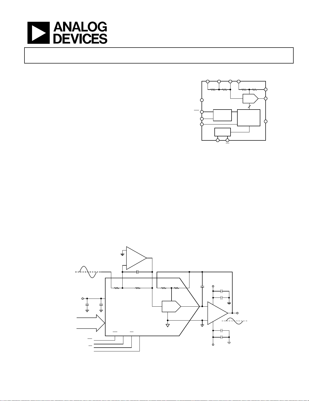
Figure 2. 16-/14-Bit, Four-Quadrant Multiplying DAC with a Minimum of External Components
+
OP2177
–
R
COMA
U1
RSRSMSB
U2A
C7
VREFA
R2R1
AD5546/AD5556
FUNCTIONAL BLOCK DIAGRAM
R1 R
R1 R2
WR
AD5546/
DD
AD5556
V
LDAC
DB0 TO DB15
Figure 1. AD5546/AD5556 Simplified Block Diagram
GENERAL DESCRIPTION
The AD5546/AD5556 are precision 16-/14-bit, multiplying, low
power, current output, parallel input digital-to-analog converters
(DACs). They operate from a single 2.7 V to 5.5 V supply with
±10 V multiplying references for four-quadrant outputs. Builtin four-quadrant resistors facilitate the resistance matching and
temperature tracking that minimize the number of components
needed for multiquadrant applications. The feedback resistor
(R
) simplifies the I-V conversion with an external buffer. The
FB
AD5546/AD5556 are packaged in compact TSSOP-28 packages
with operating temperatures from –40°C to +125°C.
The EVAL-AD5546SDZ is available for evaluating DAC perfor-
mance. For more information, see the UG-309 evaluation board
user guide.
R
R
OFSA
FBA
R
R
OFS
FB
I
OUT
GND
16-/14-BIT
DATA
One Technology Way, P.O. Box 9106, Norwood, MA 02062-9106, U.S.A.
Tel: 781.329.4700 www.analog.com
Fax: 781.461.3113 ©2004-2011 Analog Devices, Inc. All rights reserved.
+15V
C6
–
OP2177
+
–15V
V+
V–
COM
CONTROL
LOGIC
POR
MSB RS
C4
1µF
C5
0.1µF
U2B
C8
1µF
C9
0.1µF
REF R
OFS
R
OFSRFB
16/14
REGISTER
VOUT
DAC
DAC
03810-024
R
FB
I
OUT
GND
03810-001
Page 2

AD5546/AD5556 Data Sheet
TABLE OF CONTENTS
Features .............................................................................................. 1
Applications ....................................................................................... 1
Functional Block Diagram .............................................................. 1
General Description ......................................................................... 1
Revision History ............................................................................... 2
Specifications ..................................................................................... 3
Electrical Characteristics ............................................................. 3
Timing Diagram ........................................................................... 4
Absolute Maximum Ratings ............................................................ 5
ESD Caution .................................................................................. 5
Pin Configurations and Function Descriptions ........................... 6
Typical Performance Characteristics ............................................. 8
Circuit Operation ........................................................................... 10
Digital-to-Analog (DAC) Converter Section ......................... 10
Digital Section ............................................................................ 11
ESD Protection Circuits ............................................................ 11
Amplifier Selection .................................................................... 11
Reference Selection .................................................................... 11
Applications Information .............................................................. 12
Unipolar Mode ........................................................................... 12
Bipolar Mode .............................................................................. 13
AC Reference Signal Attenuator ............................................... 14
System Calibration ..................................................................... 14
Reference Selection .................................................................... 15
Amplifier Selection .................................................................... 15
Outline Dimensions ....................................................................... 17
Ordering Guide .......................................................................... 17
REVISION HISTORY
11/11—Rev. C to Rev. D
Changes to General Description Section ...................................... 1
Changes to Ordering Guide .......................................................... 18
1/11—Rev. B to Rev. C
Changes to Figure 2 .......................................................................... 1
Changes to Figure 21 ...................................................................... 13
4/10—Re
Changes to Table 1 ............................................................................ 4
Moved Timing Diagram Section and Figure 5 to
Specifications Section....................................................................... 4
Moved Table 5 Through Table 7 to Digital Section Section ....... 7
Replaced Figure 15 and Figure 16 .................................................. 9
Deleted Figure 17 and Figure 18 ..................................................... 9
Added Reference Selection Section, Amplifier Selection Section,
and Table 11 Through Table 13 .................................................... 15
9/09—Rev. 0 to Rev. A
Changes to Features Section............................................................ 1
Changes to Static Performance, Relative Accuracy,
Grade: AD5546C Parameter, Table 1 ............................................. 3
Changes to Ordering Guide .......................................................... 16
1/04—Revision 0: Initial Version
v. A to Rev. B
Rev. D | Page 2 of 20
Page 3

Data Sheet AD5546/AD5556
SPECIFICATIONS
ELECTRICAL CHARACTERISTICS
VDD = 2.7 V to 5.5 V, I
Table 1.
Parameter Symbol Conditions Min Typ Max Unit
STATIC PERFORMANCE1
Resolution N AD5546, 1 LSB = V
AD5556, 1 LSB = V
Relative Accuracy INL Grade: AD5556C ±1 LSB
Grade: AD5546B ±2 LSB
Grade: AD5546C ±1 LSB
Differential Nonlinearity DNL Monotonic ±1 LSB
Output Leakage Current I
Data = zero scale, TA = TA maximum 20 nA
Full-Scale Gain Error G
Bipolar Mode Gain Error GE Data = full scale ±1 ±4 mV
Bipolar Mode Zero-Scale
Error
Full-Scale Tempco2 TCVFS 1 ppm/°C
REFERENCE INPUT
V
Range V
REF
REF Input Resistance REF 4 5 6 kΩ
R1 and R2 Resistance R1 and R2 4 5 6 kΩ
R1-to-R2 Mismatch ∆(R1 to R2) ±0.5 ±1.5 Ω
Feedback and Offset
Resistance
Input Capacitance2 C
ANALOG OUTPUT
Output Current I
Output Capacitance2 C
LOGIC INPUT AND OUTPUT
Logic Input Low Voltage VIL VDD = 5 V 0.8 V
VDD = 3 V 0.4 V
Logic Input High Voltage VIH VDD = 5 V 2.4 V
VDD = 3 V 2.1 V
Input Leakage Current IIL 10 µA
Input Capacitance2 CIL 10 pF
INTERFACE TIMING
Data to WR Setup Time tDS VDD = 5 V 20 ns
VDD = 3 V 35 ns
Data to WR Hold Time tDH VDD = 5 V 0 ns
VDD = 3 V 0 ns
Pulse Width tWR VDD = 5 V 20 ns
WR
VDD = 3 V 35 ns
LDAC Pulse Width t
VDD = 3 V 35 ns
= virtual GND, GND = 0 V, V
OUT
V
REF
V
REF
Data = zero scale, TA = 25°C 10 nA
OUT
Data = full scale ±1 ±4 mV
FSE
G
Data = full scale ±1 ±2.5 mV
ZSE
–18 +18 V
REF
RFB, R
OFS
5 pF
REF
Data = full scale 2 mA
OUT
Code dependent 200 pF
OUT
2, 3
VDD = 5 V 20 ns
LDAC
= –10 V to 10 V, TA = full operating temperature range, unless otherwise noted.
REF
/216 = 153 µV at
REF
16 Bits
= 10 V
/214 = 610 µV at
REF
14 Bits
= 10 V
8 10 12 kΩ
Rev. D | Page 3 of 20
Page 4
AD5546/AD5556 Data Sheet
Parameter Symbol Conditions Min Typ Max Unit
t
RS Pulse Width
V
RS
V
t
WR to LDAC Delay Time
V
LWD
V
SUPPLY CHARACTERISTICS
Power Supply Range V
2.7 5.5 V
DD RANGE
Positive Supply Current IDD Logic inputs = 0 V 10 μA
Power Dissipation P
Logic inputs = 0 V 0.055 mW
DISS
Power Supply Sensitivity PSS ∆VDD = ±5% 0.003 %/%
AC CHARACTERISTICS4
Output Voltage Settling
t
S
Time
Reference Multiplying BW BW V
DAC Glitch Impulse Q V
Multiplying Feedthrough
V
OUT/VREF
V
Error
Digital Feedthrough QD
Total Harmonic Distortion THD V
Output Noise Density eN f = 1 kHz, BW = 1 Hz 12 nV/rt Hz
1
All static performance tests (except I
tied to the amplifier output. The op amp +IN is grounded, and the DAC I
2
These parameters are guaranteed by design and are not subject to production testing.
3
All input control signals are specified with tR = tF = 2.5 ns (10% to 90% of 3 V) and timed from a voltage level of 1.5 V.
4
All ac characteristic tests are performed in a closed-loop system using an AD8038 I-V converter amplifier except for THD where an AD8065 was used.
5
C6 is the C6 capacitor shown in Figure 20.
) are performed in a closed-loop system, using an external precision OP97 I-V converter amplifier. The AD554x RFB terminal is
OUT
= 5 V 20 ns
DD
= 3 V 35 ns
DD
= 5 V 0 ns
DD
= 3 V 0 ns
DD
To ±0.1% of full scale, data cycles from zero
0.5 μs
scale to full scale to zero scale
= 100 mV rms, data = full scale, C6 =5.6 pF5 6.8 MHz
REF
= 0 V, midscale minus 1 to midscale −3 nV-s
REF
= 100 mV rms, f = 10 kHz 79 dB
REF
= 1, LDAC toggles at 1 MHz
WR
= 5 V p-p, data = full-scale, f = 1 kHz –103 dB
REF
is tied to the op amp –IN. Typical values represent average readings measured at 25°C.
OUT
7 nV-s
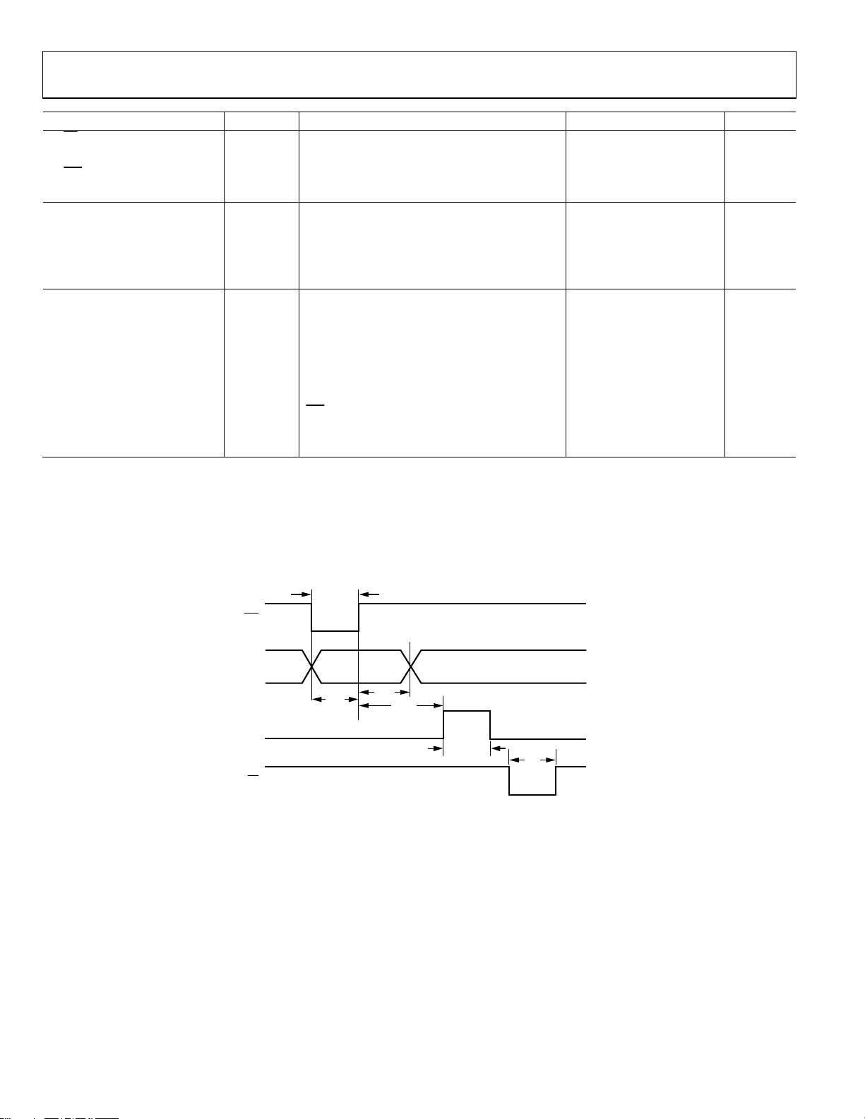
TIMING DIAGRAM
WR
DATA
LDAC
RS
t
WR
t
t
DS
DH
t
LWD
t
LDAC
Figure 3. AD5546/AD5556 Timing Diagram
t
RS
03810-005
Rev. D | Page 4 of 20
Page 5
Data Sheet AD5546/AD5556
ABSOLUTE MAXIMUM RATINGS
Table 2.
Parameter Rating
VDD to GND –0.3 V, +8 V
RFB, R
, R1, R
OFS
Logic Inputs to GND –0.3 V, +8 V
V (I
) to GND –0.3 V, VDD + 0.3 V
OUT
Input Current to Any Pin Except Supplies ±50 mA
Thermal Resistance (θJA) 128°C
Maximum Junction Temperature (TJ
Operating Temperature Range –40°C to +125°C
Storage Temperature Range –65°C to +150°C
Lead Temperature:
Vapor Phase, 60 s 215°C
Infrared, 15 s 220°C
Package Power Dissipation (T
, and REF to GND –18 V, 18 V
COM
) 150°C
MAX
J MAX
– TA)/θJA
Stresses above those listed under Absolute Maximum Ratings
may cause permanent damage to the device. This is a stress
rating only; functional operation of the device at these or any
other conditions above those listed in the operational sections
of this specification is not implied. Exposure to absolute
maximum rating conditions for extended periods may affect
device reliability.
ESD CAUTION
Rev. D | Page 5 of 20
Page 6
AD5546/AD5556 Data Sheet
03810-003
AD5546
TOP VIEW
(Not to S cale)
D7
1
V
DD
28
D6
2
D8
27
D5
3
D9
26
D4
4
D10
25
D3
5
D11
24
D2
6
D12
23
D1
7
D13
22
D0
8
D14
21
R
OFS
9
D15
20
R
FB
10
GND
19
R1
11
RS
18
R
COM
12
MSB
17
REF
13
WR
16
I
OUT
14
LDAC
15
03810-004
AD5556
TOP VIEW
(Not to S cale)
NC = NO CONNECT
D5
1
V
DD
28
D4
2
D6
27
D3
3
D7
26
D2
4
D8
25
D1
5
D9
24
D0
6
D10
23
NC
7
D11
22
NC
8
D12
21
R
OFS
9
D13
20
R
FB
10
GND
19
R1
11
RS
18
R
COM
12
MSB
17
REF
13
WR
16
I
OUT
14
LDAC
15
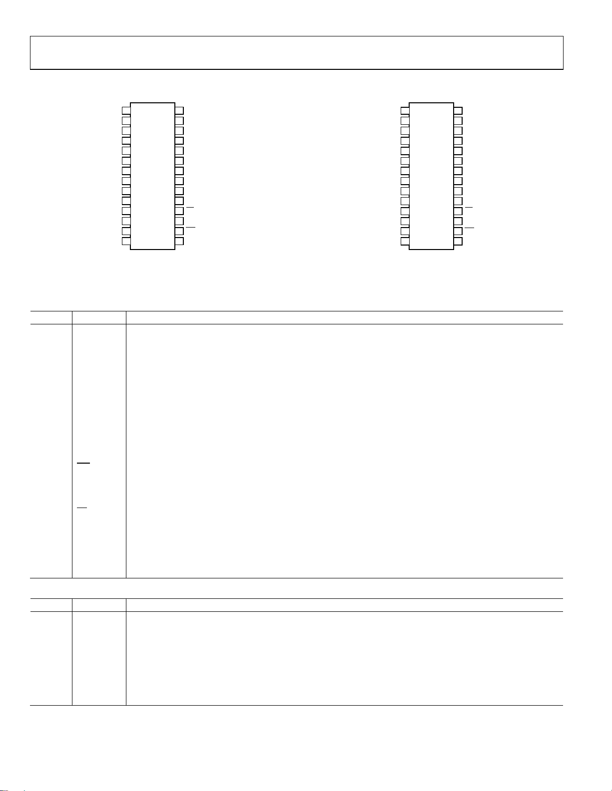
PIN CONFIGURATIONS AND FUNCTION DESCRIPTIONS
Figure 4. AD5546 Pin Configuration
Figure 5. AD5556 Pin Configuration
Table 3. AD5546 Pin Function Descriptions
Pin No. Mnemonic Description
1 to 8 D7 to D0 Digital Input Data Bits[D7: D0]. The signal level must be ≤ VDD + 0.3 V.
9 R
Bipolar Offset Resistor. Accepts up to ±18 V. In two-quadrant mode, ties to RFB. In four-quadrant mode, ties to R1
OFS
and the external reference.
10 RFB Internal Matching Feedback Resistor. Connects to the output of an external op amp for I-V conversion.
11 R1 Four-Quadrant Resistor R1. In two-quadrant mode, shorts to the REF pin. In four-quadrant mode, ties to R
12 R
Center Tap Point of Two Four-Quadrant Resistors, R1 and R2. In four-quadrant mode, ties to the inverting node of
COM
OFS
.
the reference amplifier. In two-quadrant mode, shorts to the REF pin.
13 REF DAC Reference Input in Two-Quadrant Mode and R2 Terminal in Four-Quadrant Mode. In two-quadrant mode, this
pin is the reference input with constant input resistance vs. code. In four-quadrant mode, this pin is driven by the
external reference amplifier.
14 I
DAC Current Output. Connects to the inverting node of an external op amp for I-V conversion.
OUT
15 LDAC Digital Input Load DAC Control. Signal level must be ≤ VDD + 0.3 V.
16
Write Control Digital Input in Active Low. Transfers shift-register data to the DAC register on the rising edge. The
WR
signal level must be ≤ V
+ 0.3 V.
DD
17 MSB Power-On Reset State. MSB = 0 resets at zero scale; MSB = 1 resets at midscale. The signal level must be
≤ V
+ 0.3 V.
DD
18
Reset in Active Low. Resets to zero scale if MSB = 0, and resets to midscale if MSB = 1. The signal level must be
RS
≤ V
+ 0.3 V.
DD
19 GND Analog and Digital Grounds.
20 to 21 D15 to D14 Digital Input Data Bits[D15:D14]. The signal level must be ≤ VDD + 0.3 V.
22 to 27 D13 to D8 Digital Input Data Bits[D13:D8]. The signal level must be ≤ VDD + 0.3 V.
28 VDD Positive Power Supply Input. Specified range of operation: 2.7 V to 5.5 V.
Table 4. AD5556 Pin Function Descriptions
Pin No. Mnemonic Description
1 to 6 D5 to D0
Digital Input Data Bits[D5:D0]. The signal level must be ≤ V
+0.3 V.
DD
7 to 8 NC No Connection. The user should not connect anything other than dummy pads on these terminals.
9 R
10 RFB Internal Matching Feedback Resistor. Connects to the output of an external op amp for I-V conversion.
11 R1 Four-Quadrant Resistor R1. In two-quadrant mode, shorts to the REF pin. In four-quadrant mode, ties to R
12 R
Bipolar Offset Resistor. Accepts up to ±18 V. In two-quadrant mode, ties to RFB. In four-quadrant mode, ties to R1
OFS
Center Tap Point of Two Four-Quadrant Resistors, R1 and R2. In four-quadrant mode, ties to the inverting node of
COM
and the external reference.
the reference amplifier. In two-quadrant mode, shorts to the REF pin.
Rev. D | Page 6 of 20
OFS
.
Page 7

Data Sheet AD5546/AD5556
Pin No. Mnemonic Description
13 REF DAC Reference Input in Two-Quadrant Mode and R2 Terminal in Four-Quadrant Mode. In two-quadrant mode, this
pin is the reference input with constant input resistance vs. code. In four-quadrant mode, this pin is driven by the
external reference amplifier.
14 I
15 LDAC Digital Input Load DAC Control. The signal level must be ≤ VDD + 0.3 V.
16
17 MSB Power On Reset State. MSB = 0 resets at zero scale; MSB = 1 resets at midscale. The signal level must be
18
19 GND Analog and Digital Grounds.
20 to 27 D13 to D6 Digital Input Data Bits[D13:D6]. The signal level must be ≤ VDD + 0.3 V.
28 VDD Positive Power Supply Input. Specified range of operation: 2.7 V to 5.5 V.
DAC Current Output. Connects to the inverting node of an external op amp for I-V conversion.
OUT
Write Control Digital Input in Active Low. Transfers shift-register data to the DAC register on the rising edge. The
WR
signal level must be ≤ V
+ 0.3 V.
≤ V
DD
Reset in Active Low. Resets to zero scale if MSB = 0 and resets to midscale if MSB = 1. The signal level must be
RS
≤ V
+ 0.3 V.
DD
+ 0.3 V.
DD
Rev. D | Page 7 of 20
Page 8

AD5546/AD5556 Data Sheet
TYPICAL PERFORMANCE CHARACTERISTICS
1.0
0.8
0.6
0.4
0.2
0
INL (LSB)
–0.2
–0.4
–0.6
–0.8
–1.0
0 8192 16,384 24,576 32,768 40,960 49,152 57,344 65,536
CODE (Decimal)
03810-006
1.0
0.8
0.6
0.4
0.2
0
DNL (LSB)
–0.2
–0.4
–0.6
–0.8
–1.0
0 0248 4096 6144 8192 10,240 12,288 14,336 16,384
CODE (Decimal)
03810-009
Figure 6. AD5546 Integral Nonlinearity Error
1.0
0.8
0.6
0.4
0.2
0
DNL (LSB)
–0.2
–0.4
–0.6
–0.8
–1.0
0 8192 16,384 24,576 32,768 40,960 49,152 57,344 65,536
CODE (Decimal)
Figure 7. AD5546 Differential Nonlinearity Error
1.0
0.8
0.6
0.4
0.2
0
INL (LSB)
–0.2
–0.4
–0.6
–0.8
–1.0
0 2048 4096 6144 8192 10,240 12,288 14,336 16,384
CODE (Decimal)
Figure 9. AD5556 Differential Nonlinearity Error
1.5
1.0
0.5
–0.5
LINEARITY ERROR (LSB)
–1.0
03810-007
–1.5
(LSB)
DD
SUPPLY CURRENT I
03810-008
= 2.5V
V
REF
T
= 25°C
A
INL
0
24
SUPPLY VOLTAGE VDD (V)
Figure 10. Linearity Error vs. V
5
V
= 5V
DD
T
= 25°C
A
4
3
2
1
0
0 0.5 1.0 1.5 2.0 3.0 3.52.5 4.0 4.5 5.0
LOGIC INPUT VOLTAGE VIH (V)
DNL
GE
6810
DD
03810-010
03810-011
Figure 8. AD5556 Integral Nonlinearity Error
Figure 11. Supply Current vs. Logic Input Voltage
Rev. D | Page 8 of 20
Page 9

Data Sheet AD5546/AD5556
03810-012
3.0
2.5
10k 100k 1M 10M 100M
2.0
1.5
1.0
0.5
0
SUPPLY CURRENT (mA)
CLOCK FREQUENCY (Hz)
0x5555
0x8000
0xFFFF
0x0000
03810-013
90
70
10 100 1k 10k 100k 1M
50
40
60
80
30
10
20
0
PSRR (–dB)
FREQUENCY (Hz)
VDD= 5V ± 10%
V
REF
= 10V
03810-014
LDAC
V
OUT
1
2
CH1 5.00V CH2 2.00V M 200ns A CH1 2.70V
B CH1 –6.20V
400.00ns
–4.20
–4.15
–4.10
–4.05
–4.00
–3.95
–3.90
–3.85
–3.80
–200 –100 0 100 200 300 400
TIME (ns)
V
OUT
(V)
03810-115
–18
–16
–14
–12
–10
–8
–6
–4
–2
0
2
10k 100k 1M 10M 100M
FREQUENCY (Hz)
GAIN (dB)
03810-116
Figure 12. AD5546 Supply Current vs. Clock Frequency
Figure 13. Power Supply Rejection Ratio vs. Frequency
Figure 15. AD5546 Midscale Transition
Figure 16. AD5546 Unipolar Reference Multiplying Bandwidth
Figure 14. Settling Time from Full Scale to Zero Scale
Rev. D | Page 9 of 20
Page 10

AD5546/AD5556 Data Sheet
CIRCUIT OPERATION
DIGITAL-TO-ANALOG (DAC) CONVERTER SECTION
The AD5546/AD5556 are 16-/14-bit multiplying, current output, and parallel input DACs. The devices operate from a single
2.7 V to 5.5 V supply and provide both unipolar 0 V to –V
0 V to +V
, and bipolar ±V
REF
output ranges from a –18 V to
REF
+18 V reference. In addition to the precision conversion R
commonly found in current output DACs, there are three additional precision resistors for four-quadrant bipolar applications.
The AD5546/AD5556 consist of two groups of precision R-2R
ladders, which make up the 12/10 LSBs, respectively. Furthermore, the four MSBs are decoded into 15 segments of resistor
value 2R. Figure 17 shows the architecture of the 16-bit AD5546.
Each of the 16 segments in the R-2R ladder carries an equally
weighted current of one-sixteenth of full scale. The feedback
resistor, R
, and four-quadrant resistor, R
FB
, have values of 10
OFS
kΩ. Each four-quadrant resistor, R1 and R2, equals 5 kΩ. In
four-quadrant operation, R1, R2, and an external op amp work
together to invert the reference voltage and apply it to the REF
input. With R
output can swing from –V
and RFB connected as shown in Figure 2, the
OFS
REF
to +V
REF
.
The reference voltage inputs exhibit a constant input resistance
of 5 kΩ ±20%. The DAC output, I
, impedance is code depen-
OUT
dent. External amplifier choice should take into account the
FB
REF
, or
variation of the AD5546/AD5556 output impedance. The
feedback resistance in parallel with the DAC ladder resistance
dominates output voltage noise. To maintain good analog
performance, it is recommended to bypass the power supply
with a 0.01 μF to 0.1 μF ceramic or chip capacitor in parallel
with a 1 μF tantalum capacitor. Also, to minimize gain error,
PCB metal traces between V
and RFB should match.
REF
Every code change of the DAC corresponds to a step function;
gain peaking at each output step may occur if the op amp has
limited GBP and excessive parasitic capacitance present at the
op amp inverting node. A compensation capacitor, therefore,
may be needed between the I-V op amp inverting and output
nodes to smooth the step transition. Such a compensation
capacitor should be found empirically, but a 20 pF capacitor is
generally adequate for the compensation.
The V
power is used primarily by the internal logic and to
DD
drive the DAC switches. Note that the output precision
degrades if the operating voltage falls below the specified
voltage. The user should also avoid using switching regulators
because device power supply rejection degrades at higher
frequencies.
R
REF
COM
R2
5kΩ
R1
5kΩ
R1
LDAC
2R
80kΩ2R80kΩ2R80kΩ
16 8 4
WR
R
R
R
R
R
R
40kΩ
40kΩ
40kΩ
40kΩ
40kΩ
2R
2R
2R
2R
80kΩ
80kΩ
80kΩ
RA
R
R
2R
80kΩ
80kΩ
2R
ADDRESS DECODER
DAC REGISTER
INPUT REGISTER
RB
LDAC
WR
D15 D14 D0
80kΩ
80kΩ
2R
80kΩ
R
R
2R
2R
80kΩ
40kΩ
80kΩ
80kΩ
R
40kΩ
2R
2R
80kΩ
2R
4-BIT R–2R
R
40kΩ
80kΩ
2R
80kΩ
4 MSB
15 SEGMENTS
2R
2R
80kΩ
8-BIT R–2R
R
OFS
R
FB
10kΩ 10kΩ
I
OUT
GND
RS
RS
RS
03810-019
Figure 17. 16-Bit AD5546 Equivalent R-2R DAC Circuit with Digital Section
Rev. D | Page 10 of 20
Page 11

Data Sheet AD5546/AD5556
03810-020
5kΩ
DIGITAL
INPUTS
DGND
V
DD
DIGITAL SECTION
The AD5546/AD5556 have 16-/14-bit parallel inputs. The devices are double buffered with 16-/14-bit registers. The double-buffered
feature allows the update of several AD5546/AD5556 simultaneously. For the AD5546, the input register is loaded directly from a 16-bit
controller bus when the
high. Updating the DAC register updates the DAC output with the new data (see Figure 17). To make both registers transparent, tie
low and LDAC high. The asynchronous
Table 5. AD5546 Parallel Input Data Format
MSB LSB
Bit Position B15 B14 B13 B12 B11 B10 B9 B8 B7 B6 B5 B4 B3 B2 B1 B0
Data Word D15 D14 D13 D12 D11 D10 D9 D8 D7 D6 D5 D4 D3 D2 D1 D0
Table 6. AD5556 Parallel Input Data Format
MSB LSB
Bit Position B13 B12 B11 B10 B9 B8 B7 B6 B5 B4 B3 B2 B1 B0
Data Word D13 D12 D11 D10 D9 D8 D7 D6 D5 D4 D3 D2 D1 D0
Table 7. Control Inputs
RS WR
LDAC Register Operation
0 X1 X1 Reset output to 0, with MSB pin = 0 and to midscale with MSB pin = 1.
1 0 0 Load input register with data bits.
1 1 1 Load DAC register with the contents of the input register.
1 0 1 Input and DAC registers are transparent.
1
1 1 0 No register operation.
1
X = don’t care.
WR
pin is brought low. The DAC register is updated with data from the input register when LDAC is brought
RS
pin resets the part to zero scale if the MSB pin = 0 and to midscale if the MSB pin = 1.
When LDAC and
are tied together and programmed as a pulse, the data bits are loaded into the input register on
WR
the falling edge of the pulse and then loaded into the DAC register on the rising edge of the pulse.
WR
ESD PROTECTION CIRCUITS
All logic input pins contain back-biased ESD protection Zeners
connected to ground (GND) and V
, as shown in Figure 18. As
DD
a result, the voltage level of the logic input should not be greater
than the supply voltage.
Figure 18. Equivalent ESD Protection Circuits
AMPLIFIER SELECTION
In addition to offset voltage, the bias current is important in op
amp selection for precision current output DACs. An input bias
current of 30 nA in the op amp contributes to 1 LSB in the
AD5546’s full-scale error. The OP1177 and AD8628 op amps
are good candidates for the I-V conversion.
REFERENCE SELECTION
The initial accuracy and the rated output of the voltage reference determine the full span adjustment. The initial accuracy is
usually a secondary concern in precision because it can be
trimmed. Figure 23 shows an example of a trimming circuit.
The zero scale error can also be minimized by standard op amp
nulling techniques.
The voltage reference temperature coefficient (TC) and longterm drift are primary considerations. For example, a 5 V reference with a TC of 5 ppm/
25 µV per degree Celsius. As a result, the reference that operates
at 55
Similarly, the same 5 V reference with a ±50 ppm long-term
drift means that the output may change by ±250 µV over time.
Therefore, it is practical to calibrate a system periodically to
maintain its optimum precision.
Rev. D | Page 11 of 20
o
C means that the output changes by
o
C contributes an additional 750 µV full-scale error.
Page 12

AD5546/AD5556 Data Sheet
03810-021
2
+5V
5
4
G
ND
V
IN
TRIM
U3
ADR03
V
OUT
V
DD
R1
R
OFS
R
OFS
VOUT
–2.5V TO 0V
R
FB
R
FB
C6
2.2pF
GND
U1
AD5546/AD5556
I
OUT
R2
C4
0.1µF
C5
1µF
R
COM
R1
16-/14-BIT
DATA
16-/14-BIT
DATA
REF
U2
AD8628
–
+
–5V
WRWRLDAC
LDAC
RSRSMSB
MSB
C2
0.1µF
C1
1µF
C3
0.1µF
V+
V–
APPLICATIONS INFORMATION
UNIPOLAR MODE
Two-Quadrant Multiplying Mode, V
The AD5546/AD5556 DAC architecture uses a current-steering
R-2R ladder design that requires an external reference and op
amp to convert the unipolar mode of output voltage to
AD5546
V
= –V
OUT
× D/65,536 (1)
REF
AD5556
V
= –V
OUT
× D/16,384 (2)
REF
where D is the decimal equivalent of the input code.
The output voltage polarity is opposite to the V
this case (see Figure 19). Ta b l e 8 shows the negative output vs.
code for the AD5546.
Table 8. AD5546 Unipolar Mode Negative Output vs. Code
D in Binary V
1111 1111 1111 1111 –V
1000 0000 0000 0000 –V
0000 0000 0000 0001 –V
(V)
OUT
(65,535/65,536)
REF
/2
REF
(1/65,536)
REF
0000 0000 0000 0000 0
= 0 V to –V
OUT
REF
REF
polarity in
Two-Quadrant Multiplying Mode, V
The AD5546/AD5556 are designed to operate with either
positive or negative reference voltages. As a result, positive
output can be achieved with an additional op amp, (see
Figure 20), and the output becomes
AD5546
V
OUT
= +V
× D/65,536 (3)
REF
AD5556
V
OUT
= +V
× D/16,384 (4)
REF
Table 9 shows the positive output vs. code for the AD5546.
Table 9. AD5546 Unipolar Mode Positive Output vs. Code
D in Binary V
1111 1111 1111 1111 +V
1000 0000 0000 0000 +V
0000 0000 0000 0001 +V
(V)
OUT
(65,535/65,536)
REF
/2
REF
(1/65,536)
REF
0000 0000 0000 0000 0
= 0 V to +V
OUT
REF
Figure 19. Unipolar Two-Quadrant Multiplying Mode, V
Rev. D | Page 12 of 20
= 0 to –V
OUT
REF
Page 13

Data Sheet AD5546/AD5556
03810-024
V
DD
R
OFS
R
OFSA
VOUT
R
FB
R
FBA
C6
GND
U1
AD5546/AD5556
I
OUT
R2
R1
R
COMA
R1A
16-/14-BIT
DATA
16-/14-BIT
D
ATA
VREFA
U2B
OP2177
–
+
C4
1µF
C5
0.1µF
C8
1µF
C9
0.1µF
+15V
–15V
WR
WR
LDAC
LDAC
RS
RS
MSB
MSB
C2
0.1µF
C1
1µF
V+
V–
U2A
OP2177
+
–
C7
+5V
+10V
–10V
2
5V
6
5
4
GND
V
IN
TRIM
U3
ADR03
V
OUT
5V V
DD
R1
R
OFS
R
OFS
–VREF TO +VREF
VOUT
R
FB
R
FB
C2
GND
U1
AD5546/AD5556
I
OUT
R2
U2A
OP2177
+
–
C1
–VREF +VREF
R
COM
R1
16-/14-BIT
DATA
16-/14-BIT
DATA
REF
U2B
OP2177
–
+
WRWRLDAC
LDAC
RSRSMSB
MSB
03810-002
Figure 20. Unipolar Two-Quadrant Multiplying Mode, V
Figure 21. Four-Quadrant Multiplying Mode, V
BIPOLAR MODE
Four-Quadrant Multiplying Mode, V
The AD5546/AD5556 contain on-chip all the four-quadrant
resistors necessary for the precision bipolar multiplying
operation. Such a feature minimizes the number of exponent
components to only a voltage reference, dual op amp, and
compensation capacitor (see Figure 21). For example, with a
= –V
OUT
= 0 to +V
OUT
REF
= –V
REF
to +V
REF
OUT
10 V reference, the circuit yields a precision, bipolar –10 V to
REF
to +V
REF
+10 V output.
AD5546
V
= (D/32768 − 1) × V
OUT
REF
(5)
AD5556
= (D/16384 − 1) × V
V
OUT
Table 10 shows some of the results for the 16-bit AD5546.
Rev. D | Page 13 of 20
(6)
REF
Page 14

AD5546/AD5556 Data Sheet
C8
C9
C7
ac reference signals for signal attenuation, channel equalization,
and waveform generation applications. The maximum signal
range can be up to ±18 V (see Figure 22).
SYSTEM CALIBRATION
The initial accuracy of the system can be adjusted by trimming
the voltage reference ADR0x with a digital potentiometer (see
Figure 23). The AD5170 provides an OTP (one time programmable), 8-bit adjustment that is ideal and reliable for such calibration. The Analog Devices, Inc., OTP digital potentiometer
comes with programmable software that simplifies the factory
calibration process.
ROFSA
VREFA
ROFS
16/14-BIT
–2.5V
RFBA
RFB
R
OFSA
R
OFS
16-/14-BIT
DATA
GND
IOUT
R
FBA
R
FB
GND
+15V
C4
C6
1F
C5
0.1F
–
V+
U2B
OP2177
V–
+
C8
1F
C9
0.1F
–15V
+5V
C4
C6
1µF
I
OUT
–
V+
U2B
AD8628
V–
+
C5
0.1µF
VOUT
0V TO +2.5V
VOUT
03810-0-024
Table 10. AD5546 Output vs. Code
D in Binary V
1111 1111 1111 1111 +V
1000 0000 0000 0001 +V
OUT
(32,767/32,768)
REF
(1/32,768)
REF
1000 0000 0000 0000 0
0111 1111 1111 1111 –V
0000 0000 0000 0000 –V
(1/32,768)
REF
REF
AC REFERENCE SIGNAL ATTENUATOR
Besides handling digital waveforms decoded from parallel input
data, the AD5546/AD5556 handle equally well low frequency
+
U2A
OP2177
+10V
–10V
+5V
1µF
+5V
C1
C1
1F
16/14 DATA
LDAC
MSB
0.1µF
C2
0.1F
C2
2
V
IN
U3
ADR03
TRIM
V
GND
4
16-/14-BIT
DATA
OUT
0.1µF
VDD
5
6
C3
–
C7
RCOMAR1A
U1
AD5546/AD5556
WRWRLDAC
VREFA
R2R1
RSRSMSB
Figure 22. Signal Attenuator with AC Reference
+
R3
470kΩ
U4
AD5170
10kΩ
B
R7
1kΩ
+2.5V
R1A
V
DD
AD5546/AD5556
WRWRLDAC
AD8628
–
R
COMA
U1
V+
U2A
V–
–5V
RSRSMSB
0.1µF
1µF
R2R1
LDAC
MSB
Figure 23. Full Span Calibration
Rev. D | Page 14 of 20
03810-025
Page 15

Data Sheet AD5546/AD5556
REFERENCE SELECTION
When selecting a reference for use with the AD55xx series
of current output DACs, pay attention to the output voltage
temperature coefficient specification of the reference. Choosing
a precision reference with a low output temperature coefficient
minimizes error sources. Tabl e 11 lists some of the references
available from Analog Devices that are suitable for use with this
range of current output DACs.
AMPLIFIER SELECTION
The primary requirement for the current-steering mode is an
amplifier with low input bias currents and low input offset voltage.
Because of the code-dependent output resistance of the DAC,
the input offset voltage of an op amp is multiplied by the variable
gain of the circuit. A change in this noise gain between two
adjacent digital fractions produces a step change in the output
voltage due to the amplifier’s input offset voltage. This output
voltage change is superimposed on the desired change in output
between the two codes and gives rise to a differential linearity
error, which, if large enough, can cause the DAC to be
nonmonotonic.
The input bias current of an op amp also generates an offset at
the voltage output because of the bias current flowing in the
feedback resistor, R
.
FB
Common-mode rejection of the op amp is important in voltageswitching circuits because it produces a code-dependent error
at the voltage output of the circuit.
Provided that the DAC switches are driven from true wideband
low impedance sources, they settle quickly. Consequently, the
slew rate and settling time of a voltage-switching DAC circuit is
determined largely by the output op amp. To obtain minimum
settling time in this configuration, minimize capacitance at the
V
node (the voltage output node in this application) of the
REF
DAC. This is done by using low input capacitance buffer
amplifiers and careful board design.
Analog Devices offers a wide range of amplifiers for both precision
dc and ac applications, as listed in Table 12 and Table 13.
Table 11. Suitable Analog Devices Precision References
Maximum Te mperature
Part No. Output Voltage (V) Initial Tolerance (%)
ADR01 10 0.05 3 1 20 SOIC-8
ADR01 10 0.05 9 1 20 TSOT-5, SC70-5
ADR02 5.0 0.06 3 1 10 SOIC-8
ADR02 5.0 0.06 9 1 10 TSOT-5, SC70-5
ADR03 2.5 0.1 3 1 6 SOIC-8
ADR03 2.5 0.1 9 1 6 TSOT-5, SC70-5
ADR06 3.0 0.1 3 1 10 SOIC-8
ADR06 3.0 0.1 9 1 10 TSOT-5, SC70-5
ADR420 2.048 0.05 3 0.5 1.75 SOIC-8, MSOP-8
ADR421 2.50 0.04 3 0.5 1.75 SOIC-8, MSOP-8
ADR423 3.00 0.04 3 0.5 2 SOIC-8, MSOP-8
ADR425 5.00 0.04 3 0.5 3.4 SOIC-8, MSOP-8
ADR431 2.500 0.04 3 0.8 3.5 SOIC-8, MSOP-8
ADR435 5.000 0.04 3 0.8 8 SOIC-8, MSOP-8
ADR391 2.5 0.16 9 0.12 5 TSOT-5
ADR395 5.0 0.10 9 0.12 8 TSOT-5
Drift (ppm/°C)
ISS (mA) Output Noise (µV p-p) Package(s)
Rev. D | Page 15 of 20
Page 16

AD5546/AD5556 Data Sheet
Table 12. Suitable Analog Devices Precision Op Amps
V
Maximum
Part No. Supply Voltage (V)
OP97 ±2 to ±20 25 0.1 0.5 600 SOIC-8 , PDIP-8
OP1177 ±2.5 to ±15 60 2 0.4 500 MSOP-8, SOIC-8
AD8675 ±5 to ±18 75 2 0.1 2300 MSOP-8, SOIC-8
AD8671 ±5 to ±15 75 12 0.077 3000 MSOP-8, SOIC-8
ADA4004-1 ±5 to ±15 125 90 0.1 2000 SOIC-8, SOT-23-5
AD8603 1.8 to 5 50 0.001 2.3 40 TSOT-5
AD8607 1.8 to 5 50 0.001 2.3 40 MSOP-8, SOIC-8
AD8605 2.7 to 5 65 0.001 2.3 1000 WLCSP-5, SOT-23-5
AD8615 2.7 to 5 65 0.001 2.4 2000 TSOT-23-5
AD8616 2.7 to 5 65 0.001 2.4 2000 MSOP-8, SOIC-8
OS
(µV)
Table 13. Suitable Analog Devices High Speed Op Amps
Part No. Supply Voltage (V) BW @ ACL (MHz) Slew Rate (V/µs) VOS (Max) (µV) IB (Max) (nA) Package(s)
AD8065 5 to 24 145 180 1500 0.006 SOIC-8, SOT-23-5
AD8066 5 to 24 145 180 1500 0.006 SOIC-8, MSOP-8
AD8021 5 to 24 490 120 1000 10,500 SOIC-8, MSOP-8
AD8038 3 to 12 350 425 3000 750 SOIC-8, SC70-5
ADA4899-1 5 to 12 600 310 35 100 LFCSP-8, SOIC-8
AD8057 3 to 12 325 1000 5000 500 SOT-23-5, SOIC-8
AD8058 3 to 12 325 850 5000 500 SOIC-8, MSOP-8
AD8061 2.7 to 8 320 650 6000 350 SOT-23-5, SOIC-8
AD8062 2.7 to 8 320 650 6000 350 SOIC-8, MSOP-8
AD9631 ±3 to ±6 320 1300 10,000 7000 SOIC-8, PDIP-8
IB Maximum
(nA)
0.1 Hz to 10 Hz
Noise (µV p-p) Supply Current (µA) Package(s)
Rev. D | Page 16 of 20
Page 17

Data Sheet AD5546/AD5556
COMPLIANT TO JEDEC STANDARDS MO-153-AE
28
15
141
8°
0°
SEATING
PLANE
COPLANARITY
0.10
1.20 MAX
6.40 BSC
0.65
BSC
PIN 1
0.30
0.19
0.20
0.09
4.50
4.40
4.30
0.75
0.60
0.45
9.80
9.70
9.60
0.15
0.05
OUTLINE DIMENSIONS
Figure 24. 28-Lead Thin Shrink Small Outline Package [TSSOP]
RU-28
Dimensions shown in millimeters
ORDERING GUIDE
RES
Model1
(Bit)
AD5546BRU 16 ±1 ±2 −40 to +125 28-Lead TSSOP RU-28 50
AD5546BRU-REEL7 16 ±1 ±2 −40 to +125 28-Lead TSSOP RU-28 1,000
AD5546BRUZ 16 ±1 ±2 −40 to +125 28-Lead TSSOP RU-28 50
AD5546BRUZ-REEL7 16 ±1 ±2 −40 to +125 28-Lead TSSOP RU-28 1,000
AD5546CRUZ 16 ±1 ±1 −40 to +125 28-Lead TSSOP RU-28 50
AD5546CRUZ-REEL7 16 ±1 ±1 −40 to +125 28-Lead TSSOP RU-28 1,000
AD5556CRU 14 ±1 ±1 −40 to +125 28-Lead TSSOP RU-28 50
AD5556CRU-REEL7 14 ±1 ±1 −40 to +125 28-Lead TSSOP RU-28 1,000
AD5556CRUZ 14 ±1 ±1 −40 to +125 28-Lead TSSOP RU-28 50
EVAL-AD5546SDZ Evaluation Board
1
Z = RoHS Compliant Part.
DNL
(LSB)
INL
(LSB)
Temperature
Range (°C) Package Description Package Option Ordering Quantity
Rev. D | Page 17 of 20
Page 18

AD5546/AD5556 Data Sheet
NOTES
Rev. D | Page 18 of 20
Page 19

Data Sheet AD5546/AD5556
NOTES
Rev. D | Page 19 of 20
Page 20

AD5546/AD5556 Data Sheet
NOTES
©2004-2011 Analog Devices, Inc. All rights reserved. Trademarks and
registered trademarks are the property of their respective owners.
D 03810-0-11/11(D)
Rev. D | Page 20 of 20
 Loading...