

Page 1
2.7 V to 5.5 V, Serial-Input,
VDDV
V
S
Voltage Output, Unbuffered 16-Bit DAC
FEATURES
16-bit resolution
11.8 nV/√Hz noise spectral density
1 μs settling time
1.1 nV-sec glitch energy
0.05 ppm/°C temperature drift
5 kV HBM ESD classification
0.375 mW power consumption at 3 V
2.7 V to 5.5 V single-supply operation
Hardware
50 MHz SPI-/QSPI-/MICROWIRE-/DSP-compatible interface
Power-on reset clears DAC output to zero scale
Available in 3 mm × 3 mm, 8-/10-lead LFCSP and 10-lead
MSOP
APPLICATIONS
Automatic test equipment
Precision source-measure instruments
Data acquisition systems
Medical instrumentation
Aerospace instrumentation
Communications infrastructure equipment
Industrial control
CS
and
LDAC
functions
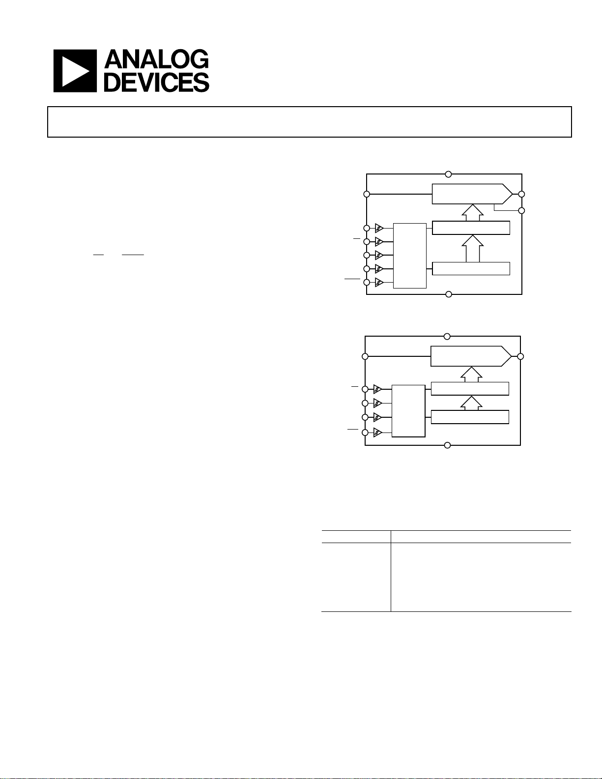
FUNCTIONAL BLOCK DIAGRAMS
REF
LOGIC
CS
DIN
SCLK
LDAC
REF
CS
DIN
CLK
CLR
AD5541A
CONTROL
LOGIC
AD5541A-1
CONTROL
LOGIC
Figure 1. AD5541A
16-BIT DAC
16-BIT DAC LATCH
SERIAL INPUT REGISTER
DGND
DD
16-BIT DAC
16-BIT DAC LATCH
SERIAL INPUT REGISITER
AD5541A
V
OUT
AGND
08516-001
V
OUT
GENERAL DESCRIPTION
The AD5541A is a single, 16-bit, serial input, unbuffered voltage
output digital-to-analog converter (DAC) that operates from a
single 2.7 V to 5.5 V supply.
The DAC output range extends from 0 V to V
monotonic, providing ±1 LSB INL accuracy at 16 bits without
adjustment over the full specified temperature range of −40°C
to +125°C. The AD5541A is available in a 3 mm × 3 mm, 10-lead
LFCSP and 10-lead MSOP. The AD5541A-1 is available in a
3 mm × 3 mm, 8-lead LFCSP.
Offering unbuffered outputs, the AD5541A achieves a 1 µs settling time with low power consumption and low offset errors.
Providing low noise performance of 11.8 nV/√Hz and low
glitch, the AD5541A is suitable for deployment across multiple
end systems.
Rev. A
Information furnished by Analog Devices is believed to be accurate and reliable. However, no
responsibility is assumed by Anal og Devices for its use, nor for any infringements of patents or ot her
rights of third parties that may result from its use. Specifications subject to change without notice. No
license is granted by implication or otherwise under any patent or patent rights of Analog Devices.
Trademarks and registered trademarks are the property of their respective owners.
and is guaranteed
REF
GND
Figure 2. AD5541A-1
The AD5541A uses a versatile 3-wire interface that is compatible
with 50 MHz SPI, QSPI™, MICROWIRE™, and DSP interface
standards.
Table 1. Related Devices
Part No. Description
AD5040/AD5060 2.7 V to 5.5 V 14-/16-bit buffed output DACs
AD5541/AD5542 2.7 V to 5.5 V 16-bit voltage output DACs
AD5781/AD5791 18-/20-bit voltage output DACs
AD5024/AD5064 4.5 V to 5.5 V, 12-/16-bit quad channel DACs
AD5061 Single, 16-bit nanoDAC, ±4 LSB INL, SOT-23
AD5542A 16-bit, bipolar, voltage output DAC
PRODUCT HIGHLIGHTS
1. 16-bit performance without adjustment.
2. 2.7 V to 5.5 V single operation.
3. Low 11.8 nV/√Hz noise spectral density.
4. Low 0.05 ppm/°C temperature drift.
5. 3 mm × 3 mm LFCSP and MSOP packaging.
One Technology Way, P.O. Box 9106, Norwood, MA 02062-9106, U.S.A.
Tel: 781.329.4700 www.analog.com
Fax: 781.461.3113 ©2010–2011 Analog Devices, Inc. All rights reserved.
08516-002
Page 2

AD5541A
TABLE OF CONTENTS
Features.............................................................................................. 1
Applications....................................................................................... 1
Functional Block Diagrams............................................................. 1
General Description......................................................................... 1
Product Highlights........................................................................... 1
Revision History ...............................................................................2
Specifications..................................................................................... 3
AC Characteristics........................................................................ 4
Timing Characteristics ................................................................ 5
Absolute Maximum Ratings............................................................ 6
ESD Caution.................................................................................. 6
Pin Configurations and Function Descriptions........................... 7
Typical Performance Characteristics............................................. 9
Terminology .................................................................................... 13
Theory of Operation ......................................................................14
Digital-to-Analog Section .........................................................14
Serial Interface............................................................................ 14
Unipolar Output Operation...................................................... 15
Output Amplifier Selection....................................................... 15
Force Sense Amplifier Selection............................................... 16
Reference and Ground............................................................... 16
Power-On Reset.......................................................................... 16
Power Supply and Reference Bypassing.................................. 16
Applications Information.............................................................. 17
Microprocessor Interfacing....................................................... 17
AD5541A to ADSP-BF531 Interface ....................................... 17
AD5541A to SPORT Interface.................................................. 17
Layout Guidelines....................................................................... 17
Galvanically Isolated Interface ................................................. 17
Decoding Multiple DACs.......................................................... 18
Outline Dimensions....................................................................... 19
Ordering Guide .......................................................................... 20
REVISION HISTORY
3/11—Rev. 0 to Rev. A
Added 10-Lead LFCSP and 8-Lead LFCSP.....................Universal
Changes to Features, General Description, and Product
Highlights Sections and Table 1 ..................................................... 1
Added Figure 2; Renumbered Sequentially .................................. 1
Changes to Logic Inputs Parameter, Table 1 ................................. 3
Changes to Figure 3.......................................................................... 5
Changes to Table 5............................................................................ 6
Changes to Table 6............................................................................ 7
Added Figure 5 and Figure 6............................................................8
Added Table 7; Renumbered Sequentially .....................................8
Changes to Figure 15...................................................................... 10
Changed V
Section.............................................................................................. 15
Updated Outline Dimensions....................................................... 18
Changes to Ordering Guide.......................................................... 18
7/10—Revision 0: Initial Version
REF
to V
– 1 LSB in Unipolar Output Operation
REF
Rev. A | Page 2 of 20
Page 3

AD5541A
SPECIFICATIONS
VDD = 2.7 V to 5.5 V, 2.5 V ≤ V
Table 2.
Parameter Min Typ Max Unit Test Condition
STATIC PERFORMANCE
Resolution 16 Bits
Relative Accuracy (INL) ±0.5 ±1.0 LSB B grade
±0.5 ±2.0 LSB A grade
Differential Nonlinearity (DNL) ±0.5 ±1.0 LSB Guaranteed monotonic
Gain Error 0.5 ±2 LSB TA = 25°C
±3 LSB −40°C < TA < +85°C
±4 LSB −40°C < TA < +125°C
Gain Error Temperature Coefficient ±0.1 ppm/°C
Zero-Code Error 0.3 ±0.7 LSB TA = 25°C
±1.5 LSB −40°C < TA < +85°C
±3 LSB −40°C < TA < +125°C
Zero-Code Temperature Coefficient ±0.05 ppm/°C
DC Power Supply Rejection Ratio ±1 LSB ∆VDD ± 10%
OUTPUT CHARACTERISTICS
Output Voltage Range 0 V
DAC Output Impedance 6.25 kΩ Tolerance typically 20%
DAC REFERENCE INPUT
3
Reference Input Range 2.0 VDD V
Reference Input Resistance 9 kΩ Unipolar operation
Reference Input Capacitance 26 pF Code 0x0000
26 pF Code 0xFFFF
LOGIC INPUTS
Input Current ±1 A
Input Low Voltage, V
0.4 V
INL
0.8 V
Input High Voltage, V
INH
1.8 V
1.3 V
Input Capacitance2 10 pF
Hysteresis Voltage2 0.15 V
POWER REQUIREMENTS
VDD 2.7 5.5 V All digital inputs at 0 V, V
IDD 125 150 µA VIH = V
V
1.8 5.5 V
LOGI C
I
15 24 µA All digital inputs at 0 V, V
LOGI C
Power Dissipation 0.625 0.825 mW
1
For 2.7 V ≤ V
2
Guaranteed by design, but not subject to production test.
3
Reference input resistance is code-dependent, minimum at 0x8555.
≤ 5.5 V: −40°C < TA < +125°C. For 1.8 V ≤ V
LOGIC
≤ VDD, AGND = DGND = 0 V, −40°C < TA < +125°C,1 unless otherwise noted.
REF
2
− 1 LSB V Unipolar operation
REF
V
= 1.8 V to 5.5 V
LOGIC
V
= 2.7 V to 5.5 V
LOGIC
V
2.4 V
≤ 2.7 V: −40°C < TA < +105°C.
LOGIC
= 4.5 V to 5.5 V
LOGIC
V
= 2.7 V to 3.6 V
LOGIC
V
= 1.8 V to 2.7 V
LOGIC
or VDD and VIL = GND
LOGI C
LOGI C
LOGI C
, or VDD
, or VDD
Rev. A | Page 3 of 20
Page 4

AD5541A
AC CHARACTERISTICS
VDD = 2.7 V to 5.5 V, 2.5 V ≤ V
Table 3.
Parameter Min Typ Max Unit Test Condition
Output Voltage Settling Time 1 s To ½ LSB of full scale, CL = 10 pF
Slew Rate 17 V/s CL = 10 pF, measured from 0% to 63%
Digital-to-Analog Glitch Impulse 1.1 nV-sec 1 LSB change around major carry
Reference −3 dB Bandwidth 2.2 MHz All 1s loaded
Reference Feedthrough 1 mV p-p All 0s loaded, V
Digital Feedthrough 0.2 nV-sec
Signal-to-Noise Ratio 92 dB
Spurious Free Dynamic Range 80 dB Digitally generated sine wave at 1 kHz
Total Harmonic Distortion 74 dB
Output Noise Spectral Density 11.8 nV/√Hz DAC code = 0x0000, frequency = 1 kHz
Output Noise 0.134 V p-p 0.1 Hz to 10 Hz
≤ VDD, AGND = DGND = 0 V, −40°C < TA < +125°C, unless otherwise noted.
REF
DAC code = 0xFFFF, frequency 10 kHz,
= 2.5 V ± 1 V p-p
V
REF
= 1 V p-p at 100 kHz
REF
Rev. A | Page 4 of 20
Page 5
AD5541A
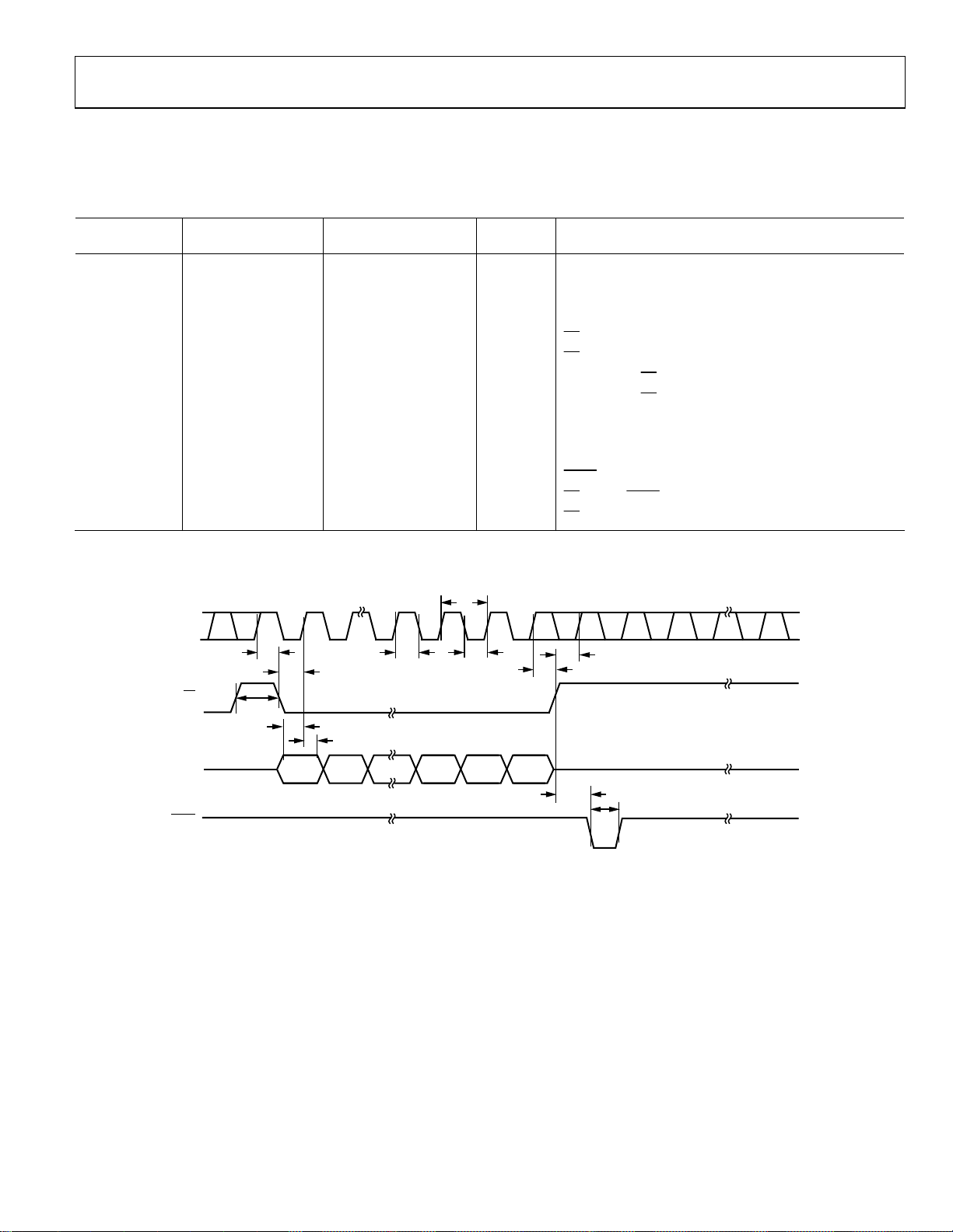
TIMING CHARACTERISTICS
VDD = 5 V, 2.5 V ≤ V
noted.
Table 4.
Parameter
f
SCLK
1, 2
14 50 MHz max SCLK cycle frequency
t1 70 20 ns min SCLK cycle time
t2 35 10 ns min SCLK high time
t3 35 10 ns min SCLK low time
t4 5 5 ns min
t5 5 5 ns min
t6 5 5 ns min
t7 10 5 ns min
t8 35 10 ns min Data setup time
t9 5 4 ns min Data hold time (V
t9 5 5 ns min Data hold time (V
t10 20 20 ns min
t11 10 10 ns min
t12 15 15 ns min
1
Guaranteed by design and characterization. Not production tested.
2
All input signals are specified with tR = tF = 1 ns/V and timed from a voltage level of (V
SCLK
REF
Limit at
1.8 ≤ V
CS
≤ VDD, V
≤ 2.7 V
LOGIC
t
12
= 90% of V
INH
t
6
t
4
t
8
t
9
LOGIC
Limit at
2.7 V ≤ V
, V
LOGIC
INL
≤ 5.5 V
t
2
= 10% of V
t
1
t
, AGND = DGND = 0 V, −40°C < TA < +105°C, unless otherwise
LOGIC
Unit Description
low to SCLK high setup
CS
high to SCLK high setup
CS
SCLK high to CS
SCLK high to CS
pulse width
LDAC
high to LDAC low setup
CS
high time between active periods
CS
+ V
)/2.
INL
INH
3
t
5
t
7
low hold time
high hold time
= 90% of VDD, V
INH
= 3 V, V
INH
INL
= 0 V)
= 10% of VDD)
INL
DIN
LDAC
DB15
t
11
t
10
08516-003
Figure 3. Timing Diagram
Rev. A | Page 5 of 20
Page 6
AD5541A
ABSOLUTE MAXIMUM RATINGS
TA = 25°C, unless otherwise noted.
Table 5.
Parameter Rating
VDD to AGND −0.3 V to +6 V
V
to DGND −0.3 V to +6 V
LOGI C
Digital Input Voltage to DGND
−0.3 V to V
DD/VLOGI C
+
0.3 V
V
to AGND −0.3 V to VDD + 0.3 V
OUT
AGND to DGND −0.3 V to +0.3 V
Input Current to Any Pin Except Supplies ±10 mA
Operating Temperature Range
Industrial (A, B Versions) −40°C to +125°C
Storage Temperature Range −65°C to +150°C
Maximum Junction Temperature (TJ max) 150°C
Package Power Dissipation (TJ max − TA)/θJA
Thermal Impedance, θJA
LFCSP (CP-10-9) 50°C/W
LFCSP (CP-8-11) 62°C/W
MSOP (RM-10) 135°C/W
Lead Temperature, Soldering
Peak Temperature1 260°C
2
ESD
1
As per JEDEC Standard 20.
2
Human body model (HBM) classification.
5 kV
Stresses above those listed under Absolute Maximum Ratings
may cause permanent damage to the device. This is a stress
rating only; functional operation of the device at these or any
other conditions above those indicated in the operational
section of this specification is not implied. Exposure to absolute
maximum rating conditions for extended periods may affect
device reliability.
ESD CAUTION
Rev. A | Page 6 of 20
Page 7

AD5541A
A
PIN CONFIGURATIONS AND FUNCTION DESCRIPTIONS
1
V
DD
V
2
OUT
REF
CS
AD5541A
3
TOP VIEW
(Not to Scale)
4
5
GND
Figure 4. AD5541A 10-Lead MSOP Pin Configuration
Table 6. AD5541A Pin Function Descriptions
Pin No. Mnemonic Description
1 VDD Analog Supply Voltage.
2 V
Analog Output Voltage from the DAC.
OUT
3 AGND Ground Reference Point for Analog Circuitry.
4 REF
Voltage Reference Input for the DAC. Connect to an external 2.5 V reference. The reference can range from
2 V to VDD.
CS
5
6 SCLK
Logic Input Signal. The chip select signal is used to frame the serial data input.
Clock Input. Data is clocked into the serial input register on the rising edge of SCLK. The duty cycle must be
between 40% and 60%.
7 DIN
Serial Data Input. This device accepts 16-bit words. Data is clocked into the serial input register on the rising edge
of SCLK.
8
LDAC Input. When this input is taken low, the DAC register is simultaneously updated with the contents of the
LDAC
serial register data.
9 DGND Digital Ground. Ground reference for digital circuitry.
10 V
Logic Power Supply.
LOGI C
10
9
8
7
6
V
LOGIC
DGND
LDAC
DIN
SCLK
08516-031
Rev. A | Page 7 of 20
Page 8

AD5541A
T
T
1V
1REF
2CS
AD5541A-1
TOP VIEW
3SCLK
(Not to Sc ale)
4DIN
NOTES
1. FOR INCREASED RELIABILI
JOINTS AND MAXIM UM THERMAL CA PABILITY,
IT IS RECOMMENDED T HAT THE PAD BE SOLDERED
TO THE SUBSTRATE, GND.
8GND
7V
DD
6V
OUT
5CLR
Y OF THE SOLDE R
Figure 5. AD5541A-1 8-Lead LFCSP Pin Configuration
08516-004
DD
2V
OUT
CS
NOTES
1. FOR INCRE ASE D RELIABILI
JOINTS AND MAXIM UM T HERMAL CAPABILI TY,
IT IS RE COMMENDED THAT THE PAD BE SOLDERED
TO THE SUBST RATE, GND.
3AGND
4REF
5
AD5541A
TOP VIEW
(Not to S c ale)
Y OF THE SOLDER
Figure 6. AD5541A 10-Lead LFCSP Pin Configuration
Table 7. AD5541A-1 and AD5541A Pin Function Descriptions
Pin No.
8-Lead LFCSP 10-Lead LFCSP
1 4 REF
Mnemonic Description
Voltage Reference Input for the DAC. Connect to an external 2.5 V reference. The
reference can range from 2 V to VDD.
2 5
CS
3 6 SCLK
Logic Input Signal. The chip select signal is used to frame the serial data input.
Clock Input. Data is clocked into the serial input register on the rising edge of SCLK.
Duty cycle must be between 40% and 60%.
4 7 DIN
Serial Data Input. This device accepts 16-bit words. Data is clocked into the serial input
register on the rising edge of SCLK.
5 N/A1
Asynchronous Clear Input. The CLR input is falling edge sensitive. When CLR is low, all
CLR
pulses are ignored. When CLR is activated, the serial input register and the DAC
LDAC
register are cleared to zero scale.
6 2 V
Analog Output Voltage from the DAC.
OUT
N/A1 9 DGND Digital Ground. Ground reference for digital circuitry.
7 1 VDD Analog Supply Voltage.
8 N/A1 GND Ground Reference Point for Both Analog and Digital Circuitry.
N/A1 3 AGND Ground Reference Point for Analog Circuitry.
N/A1 10 V
N/A1 8
Logic Power Supply.
LOGI C
LDAC Input. When this input is taken low, the DAC register is simultaneously updated
LDAC
with the contents of the serial input register.
EPAD
Exposed Pad. For increased reliability of the solder joints and maximum thermal
capability, it is recommended that the pad be soldered to the substrate, GND.
1
N/A means not applicable.
10 V
LOGIC
9DGND
8
LDAC
7DIN
6SCLK
08516-005
Rev. A | Page 8 of 20
Page 9

AD5541A
TYPICAL PERFORMANCE CHARACTERISTICS
0.50
VDD = 5V
V
= 2.5V
REF
0.25
0
–0.25
–0.50
INTEGRAL NONLINEARIT Y ( LSB)
–0.75
0 8192 16,384 24,576 32,768 40,960 49,152 57,344 65,536
CODE
Figure 7. Integral Nonlinearity vs. Code
0.25
VDD = 5V
= 2.5V
V
REF
0
–0.25
–0.50
0.50
VDD = 5V
V
= 2.5V
REF
0.25
0
–0.25
DIFFERENT IAL NONLI NE ARI TY (LSB)
–0.50
0 8192 16,384 24,576 32,768 40,960 49,152 57,344 65,536
08516-006
CODE
08516-009
Figure 10. Differential Nonlinearity vs. Code
0.75
VDD = 5V
V
= 2.5V
REF
0.50
0.25
0
–0.75
INTEGRAL NONLINEARIT Y (LSB)
–1.00
–60 –40 –20 0 20 40 60 80 100 120 140
TEMPERATURE (°C)
Figure 8. Integral Nonlinearity vs. Temperature
0.50
V
= 2.5V
REF
T
= 25°C
A
0.25
0
–0.25
LINEARIT Y E RROR (LSB)
–0.50
–0.75
234567
DNL
INL
SUPPLY VOLTAGE (V)
Figure 9. Linearity Error vs. Supply Voltage
–0.25
DIFFERENTIAL NONL INEARITY (L S B)
–0.50
–60 –40 –20 0 20 40 60 80 100 120 140
08516-007
TEMPERATURE (°C)
08516-010
Figure 11. Differential Nonlinearity vs. Temperature
0.75
VDD = 5V
T
= 25°C
A
0.50
0.25
0
LINEARIT Y E RROR (LSB)
–0.25
–0.50
012345
08516-008
DNL
INL
REFERENCE VOL T AG E (V)
6
08516-011
Figure 12. Linearity Error vs. Reference Voltage
Rev. A | Page 9 of 20
Page 10

AD5541A
3
2
VDD = 5V
V
= 2.5V
REF
T
= 25°C
A
1.5
1.0
VDD = 5V
V
= 2.5V
REF
T
= 25°C
A
1
0
–1
GAIN E RROR (LSB)
–2
–3
–100 –50 0 50 100 150
TEMPERATURE (°C)
Figure 13. Gain Error vs. Temperature
160
VDD = 5V
= 2.5V
V
REF
140
= 25°C
T
A
120
100
80
60
SUPPLY CURRENT (µA)
40
20
0
–55 –5 45 95
TEMPERATURE (°C)
Figure 14. Supply Current vs. Temperature
0.5
0
–0.5
ZERO-CODE ERRO R (LSB)
–1.0
–1.5
08516-012
Figure 16. Zero-Code Error vs. Temperature
200
TA = 25°C
150
100
SUPPLY CURRENT (µA)
50
0
012345
08516-013
–5–55 45 95
TEMPERATURE (°C)
REFERENCE VOLTAGE
V
= 5V
DD
SUPPLY VOLTAGE
V
= 2.5V
REF
VOLTAGE (V)
08516-015
6
08516-016
Figure 17. Supply Current vs. Reference Voltage or Supply Voltage
200
180
160
140
120
100
80
60
SUPPLY CURRENT (µA)
40
20
0
1.0 1.1 1.2 1.3 1.4 1.5 1.6 1.7 1.8 1.9 2.0
DIGITAL INPUT VOLTAGE (V)
Figure 15. Supply Current vs. Digital Input Voltage
08516-014
Rev. A | Page 10 of 20
200
150
100
50
REFERENCE CURRENT (µ A)
0
0 70,00060,00050,00040,00030,00020,00010,000
CODE (Decimal)
Figure 18. Reference Current vs. Code
VDD = 5V
V
= 2.5V
REF
T
= 25°C
A
08516-017
Page 11

AD5541A
V
100
DIN (5V/DIV)
90
V
10
0%
(50mV/DIV)
OUT
2µs/DIV
Figure 19. Digital Feedthrough
REF
V
DD
T
A
= 2.5V
= 5V
= 25°C
•••••••• •••• •••• •••• •••• •••• •••• •••• ••••
100
90
10
•••••••• •••• •••• •••• •••• •••• •••• •••• ••••
0%
08516-018
Figure 22. Small Signal Settling Time
V
REF
V
DD
T
A
= 25°C
= 2.5V
= 5V
0.5µs/DIV
V
(1V/DIV)
OUT
(50mV/DIV)
V
OUT
GAIN = –216
1LSB = 8.2mV
08516-021
1.236
CS
1.234
1.232
1.230
VOLTAGE (V)
1.228
V
OUT
1.226
1.224
–0.5 0 0.5 1.0 1.5 2.0
TIME (ns)
Figure 20. Digital-to-Analog Glitch Impulse
V
= 2.5V
2µs/DIV
•••••••• •••• •••• •••• •••• •••• •••• •••• ••••
100
90
10pF
50pF
100pF
200pF
REF
V
DD
T
A
= 5V
= 25°C
CS (5V/DIV)
5
0
–5
–10
–15
–20
–25
–30
5
+125°C
+25°C
–55°C
4
3
HITS
2
1
0
90 100 110 120
08516-032
I
SUPPLY (µA)
DD
08516-038
Figure 23. Analog Supply Current Histogram
6
5
4
3
HITS
2
+125°C
+25°C
–55°C
10
•••••••• •••• •••• •••• •••• •••• •••• •••• ••••
0%
Figure 21. Large Signal Settling Time
V
OUT
(0.5V/DIV)
Rev. A | Page 11 of 20
1
0
8516-020
15 16 17 18 19
AT RAILS (µA)
I
LOGIC
08516-039
Figure 24. Digital Supply Current Histogram
Page 12

AD5541A
V
10
40
20
5
0
OUTPUT NOISE (µV rms)
–5
0 20406080100120
FREQUENCY (Hz)
08516-033
0
–20
(dBm)
–40
OUT
V
–60
–80
–100
0 10,000 20,000 30,000 40,000 60,00050,000 70,000
FREQUENCY (Hz)
Figure 25. 0.1 Hz to 10 Hz Output Noise Figure 28. Total Harmonic Distortion
40
35
30
25
20
15
10
5
NOISE SPECTRAL DENSIT Y (nV rms/ Hz)
0
600 700 800 900 1000 12001100 1300 1400
FREQUENCY (Hz)
08516-034
10
0
–10
–20
(dBm)
REF
/
–30
OUT
V
–40
–50
–60
1k 10k 100k 1M 10M 100M
FREQUENCY (Hz)
Figure 26. Noise Spectral Density vs. Frequency,1 kHz Figure 29. Multiplying Bandwidth
08516-036
08516-037
14
12
10
8
6
4
2
NOISE SPECTRAL DENSITY (nV rms/ Hz)
0
9600 9700 9800 9900 10,000 10,20010,100 10,300 10,400
FREQUENCY (Hz)
Figure 27. Noise Spectral Density vs. Frequency, 10 kHz
08516-035
Rev. A | Page 12 of 20
Page 13

AD5541A
TERMINOLOGY
Relative Accuracy or Integral Nonlinearity (INL)
For the DAC, relative accuracy or INL is a measure of the
maximum deviation, in LSBs, from a straight line passing
through the endpoints of the DAC transfer function. A typical
INL vs. code plot is shown in Figure 7.
Differential Nonlinearity (DNL)
DNL is the difference between the measured change and the
ideal 1 LSB change between any two adjacent codes. A specified
differential nonlinearity of ±1 LSB maximum ensures monotonicity. A typical DNL vs. code plot is shown in Figure 10.
Gain Error
Gain error is the difference between the actual and ideal analog
output range, expressed as a percent of the full-scale range.
It is the deviation in slope of the DAC transfer characteristic
from ideal.
Gain Error Temperature Coefficient
Gain error temperature coefficient is a measure of the change
in gain error with changes in temperature. It is expressed in
ppm/°C.
Zero-Code Error
Zero-code error is a measure of the output error when zero
code is loaded to the DAC register.
Zero-Code Temperature Coefficient
This is a measure of the change in zero-code error with a
change in temperature. It is expressed in mV/°C.
Digital-to-Analog Glitch Impulse
Digital-to-analog glitch impulse is the impulse injected into the
analog output when the input code in the DAC register changes
state. It is normally specified as the area of the glitch in nV-sec
and is measured when the digital input code is changed by
1 LSB at the major carry transition. A digital-to-analog glitch
impulse plot is shown in Figure 20.
Digital Feedthrough
Digital feedthrough is a measure of the impulse injected into
the analog output of the DAC from the digital inputs of the
DAC, but it is measured when the DAC output is not updated.
CS
is held high while the SCLK and DIN signals are toggled. It
is specified in nV-sec and is measured with a full-scale code
change on the data bus, that is, from all 0s to all 1s and vice
versa. A typical digital feedthrough plot is shown in . Figure 19
Power Supply Rejection Ratio (PSRR)
PSRR indicates how the output of the DAC is affected by changes
in the power supply voltage. The power supply rejection ratio is
expressed in terms of percent change in output per percent
change in V
for full-scale output of the DAC. VDD is varied by
DD
±10%.
Reference Feedthrough
Reference feedthrough is a measure of the feedthrough from the
V
input to the DAC output when the DAC is loaded with all
REF
0s. A 100 kHz, 1 V p-p is applied to V
. Reference feedthrough
REF
is expressed in mV p-p.
Rev. A | Page 13 of 20
Page 14

AD5541A
THEORY OF OPERATION
The AD5541A is a single, 16-bit, serial input, voltage output
DAC. It operates from a single supply ranging from 2.7 V to 5 V
and consumes typically 125 µA with a supply of 5 V. Data is written
to these devices in a 16-bit word format, via a 3- or 4-wire serial
interface. To ensure a known power-up state, this part is designed
with a power-on reset function. The output is reset to 0 V.
DIGITAL-TO-ANALOG SECTION
The DAC architecture consists of two matched DAC sections.
A simplified circuit diagram is shown in Figure 30. The DAC
architecture of the AD5541A is segmented. The four MSBs of
the 16-bit data-word are decoded to drive 15 switches, E1 to
E15. Each switch connects one of 15 matched resistors to either
AGND or V
the S0 to S11 switches of a 12-bit voltage mode R-2R ladder
network.
V
REF
. The remaining 12 bits of the data-word drive
REF
R R
2R 2R
S0
2R . . . . .
S1 . . . . .2RS11
2RE12R . . . . .
E2 . . . . .
2R
E15
V
OUT
SERIAL INTERFACE
The AD5541A is controlled by a versatile 3- or 4-wire serial
interface that operates at clock rates of up to 50 MHz and is
compatible with SPI, QSPI, MICROWIRE, and DSP interface
standards. The timing diagram is shown in Figure 3. The
AD5541A has a separate serial input register from the 16-bit
DAC register that allows preloading of a new data value into the
serial input register without disturbing the present DAC output
voltage.
Input data is framed by the chip select input,
to-low transition on
CS
, data is shifted synchronously and
latched into the serial input register on the rising edge of the
serial clock, SCLK. After 16 data bits have been loaded into the
serial input register, a low-to-high transition on
contents of the shift register to the DAC register if
LDAC
low. If
CS
transfers the contents into the serial input register only.
is high at this point, a low-to-high transition on
After a new value is fully loaded in the serial input register, it
can be asynchronously transferred to the DAC register by
strobing the
LDAC
pin. Data is loaded MSB first in 16-bit
words. Data can be loaded to the part only while
CS
. After a high-
CS
transfers the
LDAC
CS
is low.
is held
12-BIT R-2R L ADDE R
Figure 30. DAC Architecture
FOUR MSBs DECO DED
INTO 15 EQUAL SEGMENTS
08516-022
With this type of DAC configuration, the output impedance is
independent of code, whereas the input impedance seen by the
reference is heavily code dependent. The output voltage is
dependent on the reference voltage, as shown in the following
equation:
V
OUT
N
2
×
DV
REF
=
where:
D is the decimal data-word loaded to the DAC register.
N is the resolution of the DAC.
For a reference of 2.5 V, the equation simplifies to the following:
×
5.2 D
=
V
OUT
This gives a V
OUT
536,65
of 1.25 V with midscale loaded and 2.5 V with
full scale loaded to the DAC.
The LSB size is V
/65,536.
REF
Rev. A | Page 14 of 20
Page 15

AD5541A
UNIPOLAR OUTPUT OPERATION
This DAC is capable of driving unbuffered loads of 60 kΩ.
Unbuffered operation results in low supply current, typically
300 A, and a low offset error. The AD5541A provides a
unipolar output swing ranging from 0 V to V
Figure 31 shows a typical unipolar output voltage circuit. The
code table for this mode of operation is shown in Table 8. The
example includes the ADR421 2.5 V reference and the AD8628
low offset and zero-drift reference buffer.
Table 8. Unipolar Code Table
DAC Latch Contents
MSB LSB Analog Output
1111 1111 1111 1111 V
1000 0000 0000 0000 V
0000 0000 0000 0001 V
× (65,535/65,536)
REF
× (32,768/65,536) = ½ V
REF
× (1/65,536)
REF
0000 0000 0000 0000 0 V
Assuming a perfect reference, the unipolar worst-case output
voltage can be calculated from the following equation:
D
V
−
UNIOUT
()
REF
GE
16
2
ZSE
where:
V
is the unipolar mode worst-case output.
OUT−UNI
D is the code loaded to DAC.
V
is the reference voltage applied to the part.
REF
V
is the gain error in volts.
GE
is the zero-scale error in volts.
V
ZSE
INL is the integral nonlinearity in volts.
REF
INLVVV
+++×=
− 1 LSB.
REF
OUTPUT AMPLIFIER SELECTION
For bipolar mode, a precision amplifier should be used and
supplied from a dual power supply. This provides the ±V
output. In a single-supply application, selection of a suitable
op amp may be more difficult because the output swing of the
amplifier does not usually include the negative rail, in this case,
AGND. This can result in some degradation of the specified
performance unless the application does not use codes near zero.
The selected op amp must have a very low offset voltage (the
DAC LSB is 38 V with a 2.5 V reference) to eliminate the need
for output offset trims. Input bias current should also be very
low because the bias current, multiplied by the DAC output
impedance (approximately 6 k), adds to the zero-code error.
Rail-to-rail input and output performance is required. For fast
settling, the slew rate of the op amp should not impede the
settling time of the DAC. Output impedance of the DAC is
constant and code independent, but to minimize gain errors,
the input impedance of the output amplifier should be as high
as possible. The amplifier should also have a 3 dB bandwidth of
1 MHz or greater. The amplifier adds another time constant to
the system, thus increasing the settling time of the output. A
higher 3 dB amplifier bandwidth results in a shorter effective
settling time of the combined DAC and amplifier.
REF
5V
1µF
0.1µF
2
V
IN
ADR421
4
V
6
OUT
SERIAL
INTERFACE
AD8628
0.1µF
V
CS
DIN
SCLK
5V
REF
DD
AD5541A
DGND AGND
0.1µF
10µF
+
AD820/
V
OP196
OUT
EXTERNAL
OP AMP
UNIPOLAR
OUTPUT
08516-023
Figure 31. Unipolar Output
Rev. A | Page 15 of 20
Page 16

AD5541A
FORCE SENSE AMPLIFIER SELECTION
Use single-supply, low noise amplifiers. A low output impedance at
high frequencies is preferred because the amplifiers must be
able to handle dynamic currents of up to ±20 mA.
REFERENCE AND GROUND
Because the input impedance is code dependent, drive the reference pin from a low impedance source. The AD5541A operates
with a voltage reference ranging from 2 V to V
below 2 V result in reduced accuracy. The full-scale output
voltage of the DAC is determined by the reference. Table 8
outlines the analog output voltage or particular digital codes.
If the application does not require separate force and sense
lines, tie the lines close to the package to minimize voltage
drops between the package leads and the internal die.
. References
DD
POWER-ON RESET
The AD5541A has a power-on reset function to ensure that the
output is at a known state on power-up. On power-up, the DAC
register contains all 0s until the data is loaded from the serial
register. However, the serial register is not cleared on power-up;
therefore, its contents are undefined. When loading data initially
to the DAC, 16 bits or more should be loaded to prevent erroneous
data appearing on the output. If more than 16 bits are loaded,
the last 16 are kept, and if less than 16 bits are loaded, bits remain
from the previous word. If the AD5541A must be interfaced
with data shorter than 16 bits, pad the data with 0s at the LSBs.
POWER SUPPLY AND REFERENCE BYPASSING
For accurate high resolution performance, it is recommended
that the reference and supply pins be bypassed with a 10 F
tantalum capacitor in parallel with a 0.1 F ceramic capacitor.
Rev. A | Page 16 of 20
Page 17

AD5541A
APPLICATIONS INFORMATION
MICROPROCESSOR INTERFACING
Microprocessor interfacing to the AD5541A is via a serial bus
that uses standard protocol that is compatible with DSP processors and microcontrollers. The communications channel requires
a 3- or 4-wire interface consisting of a clock signal, a data signal,
and a synchronization signal. The AD5541A requires a 16-bit
data-word with data valid on the rising edge of SCLK.
AD5541A TO ADSP-BF531 INTERFACE
The SPI interface of the AD5541A is designed to be easily
connected to industry-standard DSPs and microcontrollers.
Figure 32 shows how the AD5541A can be connected to the
Analog Devices, Inc., Blackfin® DSP. The Blackfin has an
integrated SPI port that can be connected directly to the SPI
pins of the AD5541A.
AD5541A
SPISELx
SCK
MOSI
ADSP-BF531
PF9
Figure 32. AD5541A to ADSP-BF531 Interface
CS
SCLK
DIN
LDAC
8516-040
AD5541A TO SPORT INTERFACE
The Analog Devices ADSP-BF527 has one SPORT serial port.
Figure 33 shows how one SPORT interface can be used to
control the AD5541A.
AD5541A
CS
SCLK
DIN
LDAC
8516-041
SPORT_TFS
SPORT_TSCK
SPORT_DTO
ADSP-BF527
Figure 33. AD5541A to SPORT Interface
GPIO0
LAYOUT GUIDELINES
In any circuit where accuracy is important, careful consideration of the power supply and ground return layout helps to
ensure the rated performance. Design the printed circuit board
(PCB) on which the AD5541A is mounted so that the analog
and digital sections are separated and confined to certain areas
of the board. If the AD5541A is in a system where multiple
devices require an analog ground-to-digital ground connection,
make the connection at one point only. Establish the star
ground point as close as possible to the device.
The AD5541A should have ample supply bypassing of 10 F
in parallel with 0.1 F on each supply located as close to the
package as possible, ideally right up against the device. The
10 F capacitors are the tantalum bead type. The 0.1 F capacitor should have low effective series resistance (ESR) and low
effective series inductance (ESI), such as the common ceramic
types, which provide a low impedance path to ground at high
frequencies to handle transient currents due to internal logic
switching.
GALVANICALLY ISOLATED INTERFACE
In many process control applications, it is necessary to provide
an isolation barrier between the controller and the unit being
controlled to protect and isolate the controlling circuitry from
any hazardous common-mode voltages that may occur. iCoupler®
products from Analog Devices provide voltage isolation in excess
of 2.5 kV. The serial loading structure of the AD5541A makes
the part ideal for isolated interfaces because the number of
interface lines is kept to a minimum. Figure 34 shows a 4-channel
isolated interface to the AD5541A using an ADuM1400. For
further information, visit http://www.analog.com/icouplers.
CONTROLLER
SERIAL
CLOCK IN
SERIAL
DATA OUT
SYNC OUT
LOAD DAC
OUT
ADuM1400
V
IA
V
IB
V
IC
V
ID
ENCODE
ENCODE DECODE
ENCODE DECODE
ENCODE DECODE
1
DECODE
V
OA
TO
SCLK
V
OB
TO
DIN
V
OC
TO
CS
V
OD
TO
LDAC
1
ADDITIONAL PINS OMITTED FOR CL ARITY.
Rev. A | Page 17 of 20
08516-042
Figure 34. Isolated Interface
Page 18

AD5541A
DECODING MULTIPLE DACS
The CS pin of the AD5541A can be used to select one of a
number of DACs. All devices receive the same serial clock and
serial data, but only one device receives the
time. The DAC addressed is determined by the decoder. There is
some digital feedthrough from the digital input lines. Using a
burst clock minimizes the effects of digital feedthrough on the
analog signal channels. shows a typical circuit. Figure 35
CS
signal at any one
SCLK
ENABLE
CODED
ADDRESS
DIN
V
DD
EN
DECODER
DGND
Figure 35. Addressing Multiple DACs
AD5541A
CS
DIN
SCLK
AD5541A
CS
DIN
SCLK
AD5541A
CS
DIN
SCLK
AD5541A
CS
DIN
SCLK
V
OUT
V
OUT
V
OUT
V
OUT
08516-030
Rev. A | Page 18 of 20
Page 19

AD5541A
OUTLINE DIMENSIONS
3.10
3.00
2.90
10
6
3.10
3.00
2.90
PIN 1
IDENTIFIER
0.95
0.85
0.75
0.15
0.05
COPLANARITY
1
0.50 BSC
0.10
COMPLIANT TO JEDEC STANDARDSMO-187-BA
Figure 36. 10-Lead Mini Small Outline Package [MSOP]
3.10
3.00 SQ
2.90
5.15
4.90
4.65
5
15° MAX
6°
0°
0.23
0.13
0.30
0.15
1.10 MAX
(RM-10)
Dimensions shown in millimeters
2.48
2.38
2.23
0.70
0.55
0.40
0.50 BSC
091709-A
PIN 1 INDEX
AREA
0.80
0.75
0.70
SEATING
PLANE
TOP VIEW
0.30
0.25
0.20
0.50
0.40
0.30
0.05 MAX
0.02 NOM
0.20 REF
6
EXPOSED
PAD
5
BOTTOM VIEW
FOR PROPER CONNECTION OF
THE EXPOSED PAD, REFER TO
THE PIN CONFIGURATION AND
FUNCTION DESCRIPTIONS
SECTION OF THIS DATA SHEET.
10
1
Figure 37. 10-Lead Lead Frame Chip Scale Package [LFCSP_WD]
3 mm × 3 mm Body, Very Very Thin, Dual Lead
(CP-10-9)
Dimensions shown in millimeters
1.74
1.64
1.49
P
N
I
1
A
R
O
T
N
I
D
C
I
)
5
1
.
0
R
(
121009-A
Rev. A | Page 19 of 20
Page 20

AD5541A
3.10
3.00 SQ
2.90
PIN 1 INDEX
AREA
0.50
0.40
0.30
TOP VIEW
0.80
0.75
0.70
SEATING
PLANE
0.30
0.25
0.20
COMPLIANTTOJEDEC STANDARDS MO-229-WEED
0.05 MAX
0.02 NOM
COPLANARITY
0.203 REF
0.08
2.44
2.34
2.24
5
EXPOSED
PAD
4
BOTTOM VIEW
FOR PROPER CONNECTION OF
THE EXPOSED PAD, REFER TO
THE PIN CONFIGURATION AND
FUNCTION DESCRIPTIONS
SECTION OF THIS DATA SHEET.
0.50 BSC
8
1
1.70
1.60
1.50
N
I
1
P
R
C
I
A
O
T
N
I
D
)
5
1
.
R
0
(
01-24-2011-B
Figure 38. 8-Lead Lead Frame Chip Scale Package [LFCSP_WD]
3 mm × 3 mm Body, Very Very Thin, Dual Lead
(CP-8-11)
Dimensions shown in millimeters
ORDERING GUIDE
Model1 INL DNL
Reset to Code Temperature Range Package Description
AD5541ABRMZ ±1 LSB ±1 LSB Zero Scale −40°C to +125°C 10-Lead MSOP RM-10 DEQ
AD5541ABRMZ-REEL7 ±1 LSB ±1 LSB Zero Scale −40°C to +125°C 10-Lead MSOP RM-10 DEQ
AD5541AARMZ ±2 LSB ±1 LSB Zero Scale −40°C to +125°C 10-Lead MSOP RM-10
AD5541AARMZ-REEL7 ±2 LSB ±1 LSB Zero Scale −40°C to +125°C 10-Lead MSOP RM-10
AD5541AACPZ-REEL7 ±2 LSB ±1 LSB Zero Scale −40°C to +125°C 10-lead LFCSP_WD CP-10-9
AD5541ABCPZ-REEL7 ±1 LSB ±1 LSB Zero Scale −40°C to +125°C 10-lead LFCSP_WD CP-10-9
AD5541ABCPZ-500RL7 ±1 LSB ±1 LSB Zero Scale −40°C to +125°C 10-lead LFCSP_WD CP-10-9
AD5541ABCPZ-1-RL7 ±1 LSB ±1 LSB Zero Scale −40°C to +125°C 8-lead LFCSP_WD CP-8-11
EVAL-AD5541ASDZ AD5541A Evaluation Board
Power-On
1
Z = RoHS Compliant Part.
Package
Option
Branding
Code
DER
DER
DER
DEQ
DEQ
DFG
©2010–2011 Analog Devices, Inc. All rights reserved. Trademarks and
registered trademarks are the property of their respective owners.
D08516-0-3/11(A)
Rev. A | Page 20 of 20
 Loading...