

Page 1
2.7 V to 5.5 V, Serial-Input,
V
S
V
FEATURES
Full 16-bit performance
3 V and 5 V single-supply operation
Low 0.625 mW power dissipation
1 μs settling time
Unbuffered voltage output capable of driving 60 kΩ
loads directly
SPI-/QSPI-/MICROWIRE-compatible interface standards
Power-on reset clears DAC output to 0 V (unipolar mode)
5 kV HBM ESD classification
APPLICATIONS
Digital gain and offset adjustment
Automatic test equipment
Data acquisition systems
Industrial process control
Voltage-Output, 16-Bit DACs
AD5541/AD5542
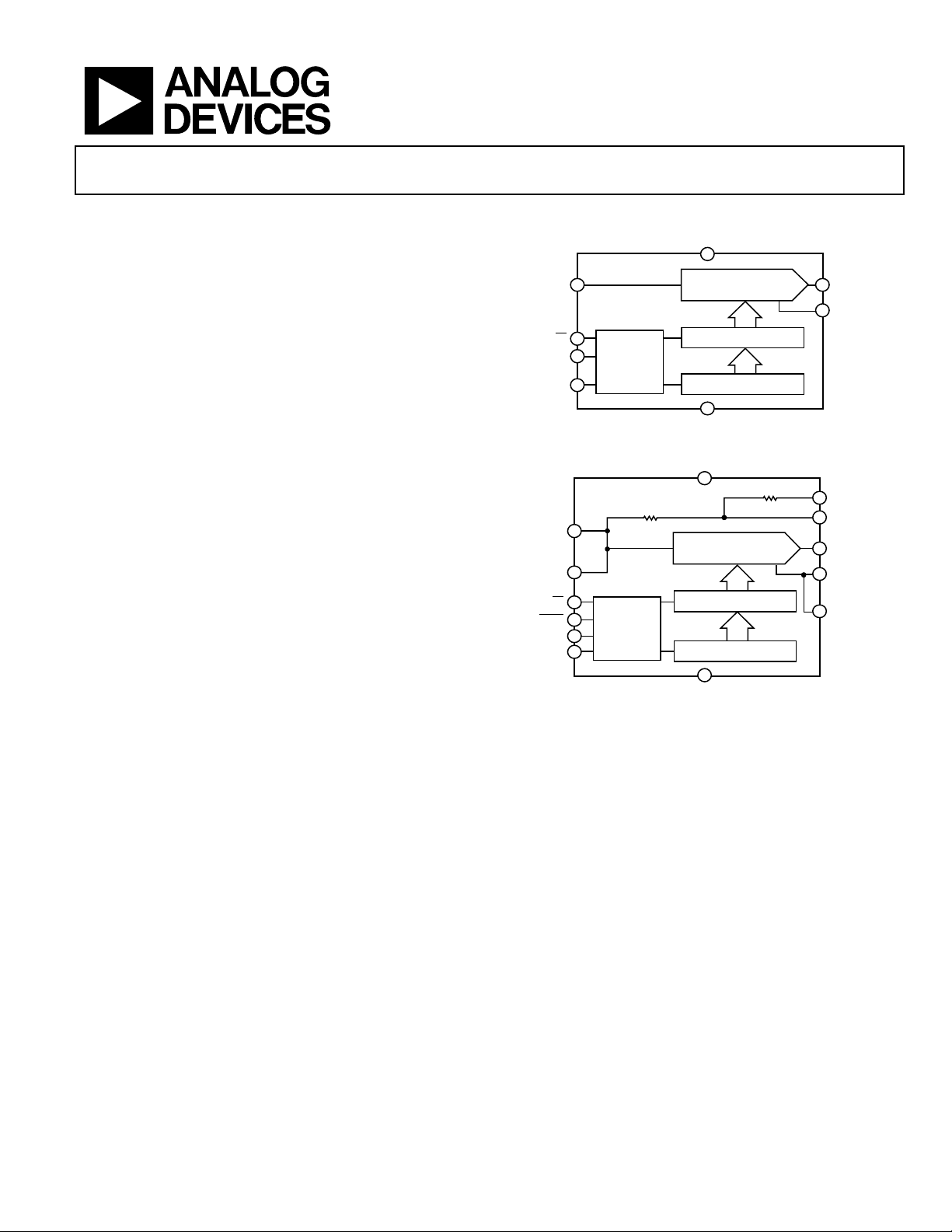
FUNCTIONAL BLOCK DIAGRAMS
DD
8
REF
CLK
REFF
REFS
DIN
CS
3
4
6
5
6
5
AD5541
CONTROL
LOGIC
AD5542
16-BIT DAC LATCH
SERIAL INPUT REGISITER
DGND
Figure 1. AD5541
DD
14
R
INV
16-BIT DAC
7
16-BIT DAC
R
FB
1
2
1
13
2
3
V
OUT
AGND
RFB
INV
V
OUT
AGNDF
07557-001
GENERAL DESCRIPTION
The AD5541/AD5542 are single, 16-bit, serial input, voltage
output digital-to-analog converters (DACs) that operate from
a single 2.7 V to 5.5 V supply. The DAC output range extends
from 0 V to V
These DACs are guaranteed monotonic, providing 1 LSB INL at
16 bits without adjustment over the full temperature range.
Offering unbuffered outputs, the AD5541/AD5542 achieve low
power consumption and low offset errors.
The AD5542 can be operated in bipolar mode, which generates
a ±V
output swing. The AD5542 also includes Kelvin sense
REF
connections for the reference and analog ground pins to reduce
layout sensitivity.
REF
.
CS
LDAC
SCLK
DIN
11
10
7
8
CONTROL
LOGIC
16-BIT DAC LATCH
SERIAL INPUT REGISITER
12
DGND
4
AGNDS
07557-002
Figure 2. AD5542
The AD5541/AD5542 utilize a versatile 3-wire interface that is
compatible with SPI, QSPI™, MICROWIRE™ and DSP interface
standards. The AD5541/AD5542 are available in 8-lead and
14-lead SOIC packages.
PRODUCT HIGHLIGHTS
1. Single-Supply Operation. The AD5541 and AD5542 are
fully specified and guaranteed for a single 2.7 V to 5.5 V
supply.
2. Low Power Consumption. These parts consume typically
0.6 mW with a 5 V supply.
3. 3-Wire Serial Interface.
4. Unbuffered Output Capable of Driving 60 kΩ Loads. This
reduces power consumption because there is no internal
buffer to drive.
5. Power-On Reset Circuitry.
Rev. C
Information furnished by Analog Devices is believed to be accurate and reliable. However, no
responsibility is assumed by Analog Devices for its use, nor for any infringements of patents or other
rights of third parties that may result from its use. Specifications subject to change without notice. No
license is granted by implication or otherwise under any patent or patent rights of Analog Devices.
Trademarks and registered trademarks are the property of their respective owners.
One Technology Way, P.O. Box 9106, Norwood, MA 02062-9106, U.S.A.
Tel: 781.329.4700 www.analog.com
Fax: 781.461.3113 ©2008–2010 Analog Devices, Inc. All rights reserved.
Page 2

AD5541/AD5542
TABLE OF CONTENTS
Features .............................................................................................. 1
Applications ....................................................................................... 1
Functional Block Diagrams ............................................................. 1
General Description ......................................................................... 1
Product Highlights ........................................................................... 1
Revision History ............................................................................... 2
Specifications ..................................................................................... 3
Timing Characteristics ................................................................ 4
Absolute Maximum Ratings ............................................................ 5
ESD Caution .................................................................................. 5
Pin Configurations and Function Descriptions ........................... 6
Typical Performance Characteristics ............................................. 7
Terminology .................................................................................... 10
Theory of Operation ...................................................................... 11
Digital-to-Analog Section ......................................................... 11
Serial Interface ............................................................................ 11
Unipolar Output Operation ...................................................... 11
Bipolar Output Operation ......................................................... 12
Output Amplifier Selection ....................................................... 12
Force Sense Amplifier Selection ............................................... 12
Reference and Ground ............................................................... 12
Power-On Reset .......................................................................... 13
Power Supply and Reference Bypassing .................................. 13
Microprocessor Interfacing ........................................................... 14
AD5541/AD5542 to ADSP-21xx Interface ............................. 14
AD5541/AD5542 to 68HC11/68L11 Interface ....................... 14
AD5541/AD5542 to MICROWIRE Interface ........................ 14
AD5541/AD5542 to 80C51/80L51 Interface .......................... 14
Applications Information .............................................................. 15
Optocoupler Interface ................................................................ 15
Decoding Multiple AD5541/AD5542s .................................... 15
Outline Dimensions ....................................................................... 16
Ordering Guide .......................................................................... 17
REVISION HISTORY
4/10—Rev. B to Rev. C
Changes to General Description Section ...................................... 1
Changes to Features List .................................................................. 1
Changes to Product Highlights ....................................................... 1
Changes to Table 1 ............................................................................ 3
Changes to Table 3 ............................................................................ 5
Changes to Figure 16, Figure 17, and Figure 19 ....................... 8, 9
Changes to Theory of Operations Section .................................. 11
Changes to Microprocessor Interfacing Section ........................ 14
Changes to Outline Dimensions ................................................... 16
Changes to Ordering Guide .......................................................... 17
8/08—Rev. A to Rev. B
Updated Format .................................................................. Universal
Changes to Timing Characteristics Section .................................. 4
Changes to Table 3 ............................................................................ 5
Updated Outline Dimensions ....................................................... 16
Changes to Ordering Guide .......................................................... 17
10/99—Rev. 0 to Rev. A
Rev. C | Page 2 of 20
Page 3

AD5541/AD5542
SPECIFICATIONS
VDD = 2.7 V to 5.5 V, 2.5 V ≤ V
Table 1.
Parameter1 Min Typ Max Unit Test Conditions
STATIC PERFORMANCE
Resolution 16 Bits
Relative Accuracy (INL) ±0.5 ±1.0 LSB L, C grades
±0.5 ±2.0 LSB B, J grades
±0.5 ±4.0 LSB A grade
Differential Nonlinearity (DNL) ±0.5 ±1.0 LSB Guaranteed monotonic
±1.5 LSB J grade
Gain Error +0.5 ±2 LSB TA = 25°C
±3 LSB
Gain Error Temperature Coefficient ±0.1 ppm/°C
Unipolar Zero Code Error ±0.3 ±0.7 LSB TA = 25°C
±1.5 LSB
Unipolar Zero Code Temperature Coefficient ±0.05 ppm/°C
AD5542
Bipolar Resistor Matching 1.000 Ω/Ω RFB/R
±0.0015 ±0.0076 % Ratio error
Bipolar Zero Offset Error ±1 ±5 LSB TA = 25°C
±6 LSB
Bipolar Zero Temperature Coefficient ±0.2 ppm/°C
Bipolar Zero Code Offset Error ±1 ±5 LSB TA = 25°C
Bipolar Gain Error +1 ±5 LSB TA = 25°C
Bipolar Gain Temperature Coefficient ±0.1 ppm/°C
OUTPUT CHARACTERISTICS
Output Voltage Range 0 V
−V
Output Voltage Settling Time 1 μs To 1/2 LSB of FS, CL = 10 pF
Slew Rate 17 V/μs CL = 10 pF, measured from 0% to 63%
Digital-to-Analog Glitch Impulse 1.1 nV-sec 1 LSB change around the major carry
Digital Feedthrough 0.2 nV-sec All 1s loaded to DAC, V
DAC Output Impedance 6.25 kΩ Tolerance typically 20%
Power Supply Rejection Ratio ±1.0 LSB ΔVDD ± 10%
DAC REFERENCE INPUT
Reference Input Range 2.0 VDD V
Reference Input Resistance2 9 kΩ Unipolar operation
7.5 kΩ AD5542, bipolar operation
LOGIC INPUTS
Input Current ±1 μA
Input Low Voltage, V
Input High Voltage, V
Input Capacitance3 10 pF
Hysteresis Voltage3
REFERENCE 3
Reference −3 dB Bandwidth 2.2 MHz All 1s loaded
Reference Feedthrough 1 mV p-p All 0s loaded, V
Signal-to-Noise Ratio 92 dB
Reference Input Capacitance 26 pF Code 0x0000
26 pF Code 0xFFFF
0.8 V
INL
2.4 V
INH
≤ VDD, AGND = DGND = 0 V. All specifications TA = T
REF
±6
±6
− 1 LSB V Unipolar operation
REF
V
REF
− 1 LSB V AD5542 bipolar operation
REF
0.15 V
Rev. C | Page 3 of 20
MIN
LSB
to T
, unless otherwise noted.
MAX
INV
LSB
, typically RFB = R
= 1 V p-p at 100 kHz
REF
= 28 kΩ
INV
= 2.5 V
REF
Page 4
AD5541/AD5542
Parameter
1
Min Typ Max Unit Test Conditions
POWER REQUIREMENTS Digital inputs at rails
VDD 2.7 5.5 V
IDD 125 150 μA
Power Dissipation 0.625 0.825 mW
1
Temperature ranges are as follows: A, B, C versions: −40°C to +85°C; J, L versions: 0°C to 70°C.
2
Reference input resistance is code-dependent, minimum at 0x8555.
3
Guaranteed by design, not subject to production test.
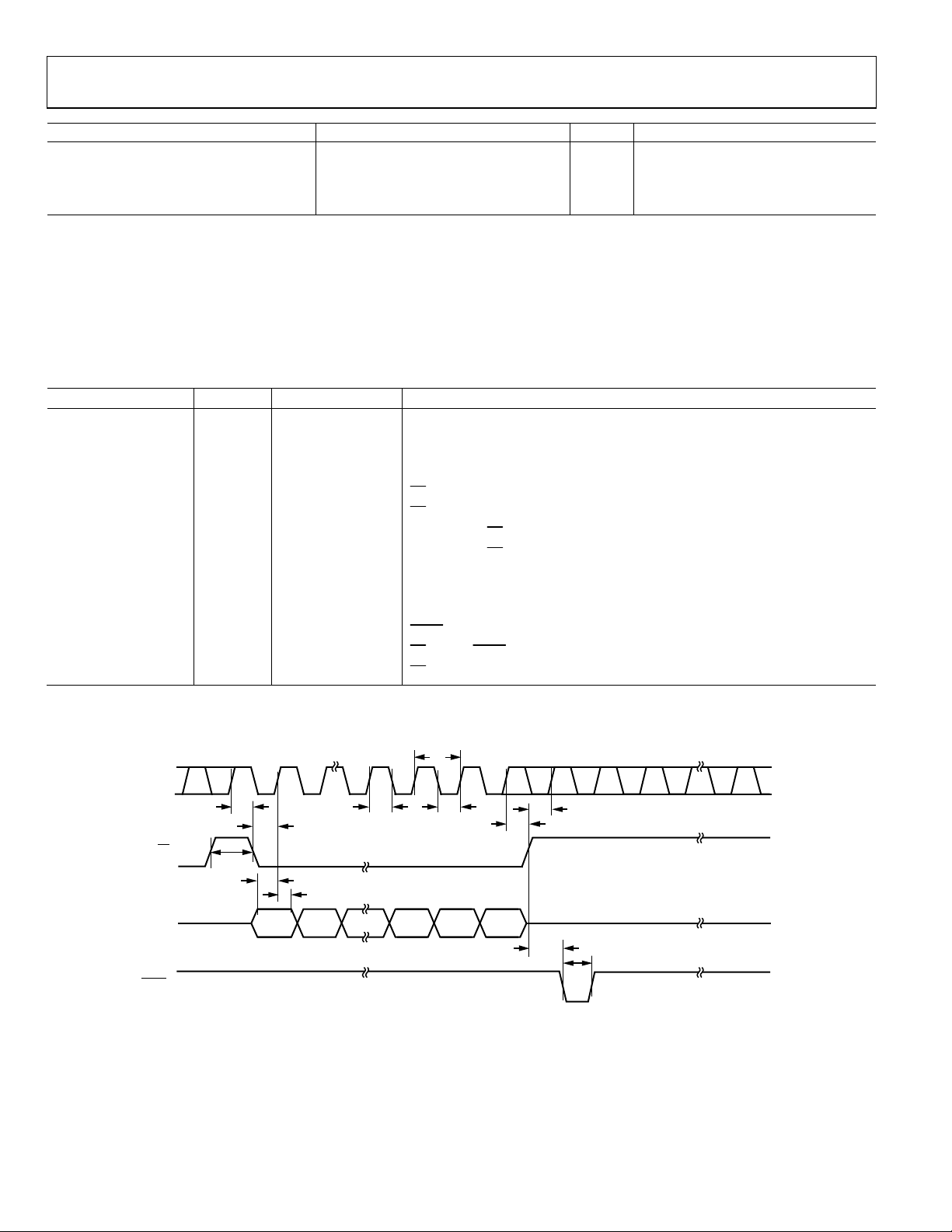
TIMING CHARACTERISTICS
VDD = 2.7 V to 5.5 V ±10%, V
+85°C, unless otherwise noted.
Table 2.
1, 2
Parameter
f
25 MHz max SCLK cycle frequency
SCLK
t1 40 ns min SCLK cycle time
t2 20 ns min SCLK high time
t3 20 ns min SCLK low time
t4 10 ns min
t5 15 ns min
t6 30 ns min
t7 20 ns min
t8 15 ns min Data setup time
t9 4 ns min Data hold time (V
t9 7.5 ns min Data hold time (V
t10 30 ns min
t11 30 ns min
t12 30 ns min
1
Guaranteed by design and characterization. Not production tested
2
All input signals are specified with tR = tF = 1 ns/V and timed from a voltage level of (V
SCLK
CS
= 2.5 V, V
REF
= 3 V and 90% of VDD, V
INH
= 0 V and 10% of VDD, AGND = DGND = 0 V; −40°C < TA <
INL
Limit Unit Description
low to SCLK high setup
CS
high to SCLK high setup
CS
SCLK high to CS
SCLK high to CS
pulsewidth
LDAC
high to LDAC low setup
CS
high time between active periods
CS
t
1
t
6
t
4
t
12
t
8
t
5
t
2
t
3
low hold time
high hold time
INH
INH
+ V
)/2.
INL
INH
= 90% of VDD, V
= 3V, V
t
7
= 0 V)
INL
t
5
= 10% of VDD)
INL
DIN
LDAC*
*AD5542 ONLY. CAN BE TIED PERMANENT LY LOW IF REQUIRE D.
DB15
Figure 3. Timing Diagram
Rev. C | Page 4 of 20
t
11
t
10
07557-003
Page 5
AD5541/AD5542
ABSOLUTE MAXIMUM RATINGS
TA = 25°C, unless otherwise noted.
Table 3.
Parameter Rating
VDD to AGND −0.3 V to +6 V
Digital Input Voltage to DGND −0.3 V to VDD + 0.3 V
V
to AGND −0.3 V to VDD + 0.3 V
OUT
AGND, AGNDF, AGNDS to DGND −0.3 V to +0.3 V
Input Current to Any Pin Except Supplies ±10 mA
Operating Temperature Range
Industrial (A, B, C Versions) −40°C to +85°C
Commercial (J, L Versions) 0°C to 70°C
Storage Temperature Range −65°C to +150°C
Maximum Junction Temperature (TJ max) 150°C
Package Power Dissipation ( TJ max – TA)/θJA
Thermal Impedance, θJA
SOIC (R-8) 149.5°C/W
SOIC (R-14) 104.5°C/W
Lead Temperature, Soldering
Peak Temperature1 260°C
ESD2 5 kV
1
As per JEDEC Standard 20.
2
HBM Classification
Stresses above those listed under Absolute Maximum Ratings
may cause permanent damage to the device. This is a stress
rating only; functional operation of the device at these or any
other conditions above those indicated in the operational
section of this specification is not implied. Exposure to absolute
maximum rating conditions for extended periods may affect
device reliability.
ESD CAUTION
Rev. C | Page 5 of 20
Page 6
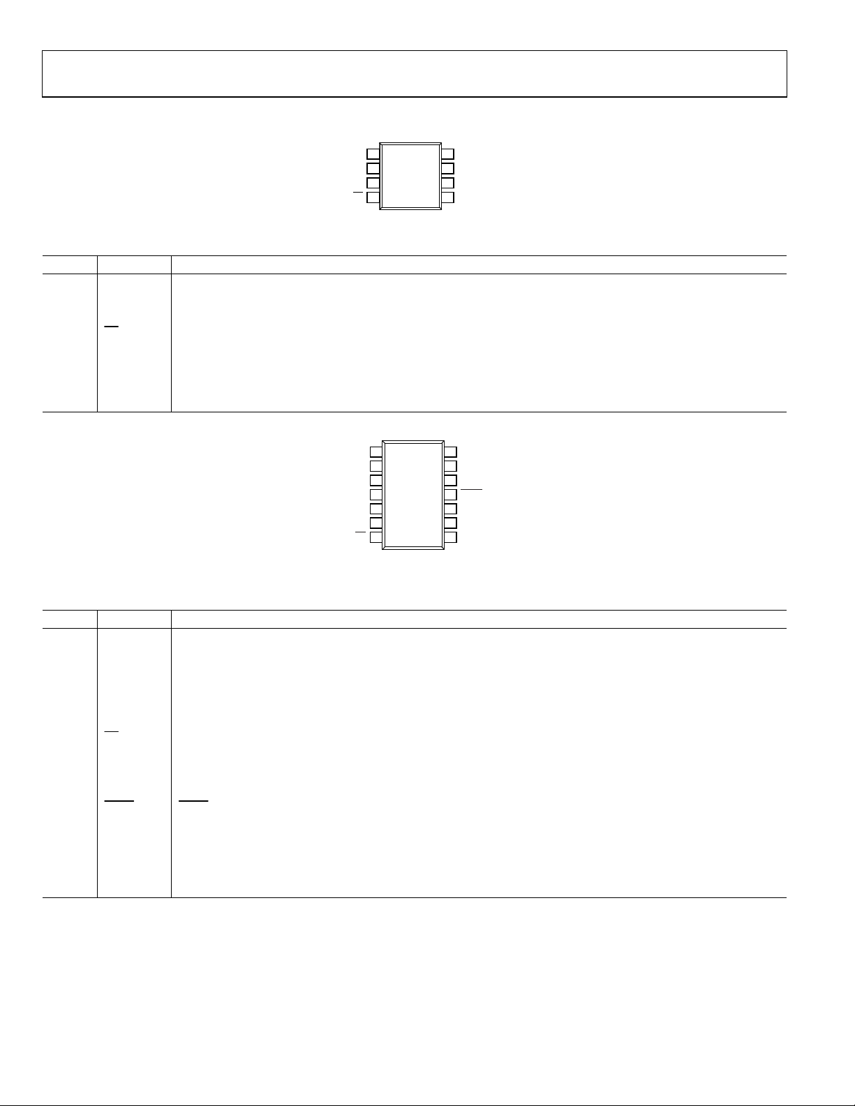
AD5541/AD5542
A
PIN CONFIGURATIONS AND FUNCTION DESCRIPTIONS
V
1
OUT
CS
AD5541
2
3
TOP VIEW
(Not to S cale)
4
AGND
REF
Figure 4. AD5541 Pin Configuration
Table 4. AD5541 Pin Function Descriptions
Pin No. Mnemonic Description
1 V
Analog Output Voltage from the DAC.
OUT
2 AGND Ground Reference Point for Analog Circuitry.
3 REF Voltage Reference Input for the DAC. Connect to an external 2.5 V reference. Reference can range from 2 V to VDD.
CS
4
Logic Input Signal. The chip select signal is used to frame the serial data input.
5 SCLK Clock Input. Data is clocked into the input register on the rising edge of SCLK. Duty cycle must be between 40% and 60%.
6 DIN Serial Data Input. This device accepts 16-bit words. Data is clocked into the input register on the rising edge of SCLK.
7 DGND Digital Ground. Ground reference for digital circuitry.
8 VDD Analog Supply Voltage, 5 V ± 10%.
RFB
1
V
2
OUT
3
AGNDF
GNDS
REFS
REFF
Figure 5. AD5542 Pin Configuration
AD5542
TOP VIEW
4
(Not to Scale)
5
6
7
CS
NC = NO CONNECT
8
7
6
5
14
13
12
11
10
9
8
V
DD
DGND
DIN
SCLK
V
DD
INV
DGND
LDAC
DIN
NC
SCLK
07557-004
07557-005
Table 5. AD5542 Pin Function Descriptions
Pin No. Mnemonic Description
1 RFB Feedback Resistor Pin. In bipolar mode, connect this pin to the external op amp output.
2 V
Analog Output Voltage from the DAC.
OUT
3 AGNDF Ground Reference Point for Analog Circuitry (Force).
4 AGNDS Ground Reference Point for Analog Circuitry (Sense).
5 REFS Voltage Reference Input (Sense) for the DAC. Connect to an external 2.5 V reference. Reference can range from 2 V to VDD.
6 REFF Voltage Reference Input (Force) for the DAC. Connect to an external 2.5 V reference. Reference can range from 2 V to VDD.
CS
7
Logic Input Signal. The chip select signal is used to frame the serial data input.
8 SCLK Clock Input. Data is clocked into the input register on the rising edge of SCLK. Duty cycle must be between 40% and 60%.
9 NC No Connect.
10 DIN Serial Data Input. This device accepts 16-bit words. Data is clocked into the input register on the rising edge of SCLK.
11
LDAC Input. When this input is taken low, the DAC register is simultaneously updated with the contents of the
LDAC
input register.
12 DGND Digital Ground. Ground reference for digital circuitry.
13 INV
Connected to the Internal Scaling Resistors of the DAC. Connect the INV pin to external op amps inverting input in
bipolar mode.
14 VDD Analog Supply Voltage, 5 V ± 10%.
Rev. C | Page 6 of 20
Page 7

AD5541/AD5542
TYPICAL PERFORMANCE CHARACTERISTICS
0.50
VDD = 5V
V
= 2.5V
REF
0.25
0
–0.25
–0.50
INTEGRAL NONLINEARIT Y ( LSB)
–0.75
0 8192 16384 24576 32768 40960 49152 57344 65536
CODE
Figure 6. Integral Nonlinearity vs. Code Figure 9. Differential Nonlinearity vs. Code
0.25
VDD = 5V
= 2.5V
V
REF
0
–0.25
–0.50
0.50
VDD = 5V
V
= 2.5V
REF
0.25
0
–0.25
DIFFERENT IAL NONLI NE ARI TY (LSB)
–0.50
0 8192 16384 24576 32768 40960 49152 57344 65536
07557-006
0.75
VDD = 5V
V
= 2.5V
REF
0.50
0.25
0
CODE
07557-009
–0.75
INTEGRAL NONLINEARIT Y (LSB)
–1.00
–60 –40 –20 0 20 40 60 80 100 120 140
TEMPERATURE (°C)
07557-007
–0.25
DIFFERENTIAL NONL INEARITY (L S B)
–0.50
–60 –40 –20 0 20 40 60 80 100 120 140
TEMPERATURE (°C)
Figure 7. Integral Nonlinearity vs. Temperature Figure 10. Differential Nonlinearity vs. Temperature
0.50
V
= 2.5V
REF
T
= 25°C
A
0.25
0
–0.25
LINEARIT Y E RROR (LSB)
–0.50
–0.75
234567
DNL
INL
SUPPLY VOLTAGE (V)
07557-008
0.75
VDD = 5V
T
= 25°C
A
0.50
0.25
0
LINEARIT Y E RROR (LSB)
–0.25
–0.50
012345
DNL
INL
REFERENCE VOL T AG E (V)
Figure 8. Linearity Error vs. Supply Voltage Figure 11. Linearity Error vs. Reference Voltage
07557-010
6
07557-011
Rev. C | Page 7 of 20
Page 8

AD5541/AD5542
ZERO-CODE ERRO R (LSB)
0.15
0.10
0.05
–0.05
–0.10
–0.15
VDD = 5V
V
= 2.5V
REF
T
= 25°C
A
0
–40 25 85
TEMPERATURE (°C)
Figure 15. Zero-Code Error vs. Temperature
08898-015
0
–0.1
–0.2
–0.3
–0.4
–0.5
–0.6
GAIN E RROR (LSB)
–0.7
–0.8
–0.9
–40 25 85
TEMPERATURE (°C)
VDD = 5V
V
= 2.5V
REF
T
= 25°C
A
08898-012
Figure 12. Gain Error vs. Temperature
132
VDD = 5V
V
= 2.5V
REF
130
T
= 25°C
A
128
126
124
122
SUPPLY CURRENT ( µ A)
120
118
116
–40 25 85
TEMPERATURE ( °C)
Figure 13. Supply Current vs. Temperature
200
180
160
140
120
100
80
60
SUPPLY CURRENT (µ V)
40
20
0
1 2 3 4 5 6 7 8 9 10 11 12 13 14 15 16 17 18 19 20 21
DIGITAL I NPUT VOLTAGE (V)
Figure 14. Supply Current vs. Digital Input Voltage
2.0
TA = 25°C
1.5
1.0
SUPPLY CURRENT (µA)
0.5
0
08898-013
REFERENCE VOLTAGE
V
= 5V
DD
SUPPLY VOLTAGE
V
= 2.5V
REF
0123456
VOLTAGE (V)
08898-016
Figure 16. Supply Current vs. Reference Voltage or Supply Voltage
200
150
100
50
REFERENCE CURRENT (µ A)
0
0 70,00060,00050,00040,00030,00020,00010,000
08898-014
CODE (Decimal)
VDD = 5V
V
= 2.5V
REF
T
= 25°C
A
08898-017
Figure 17. Reference Current vs. Code
Rev. C | Page 8 of 20
Page 9

AD5541/AD5542
V
REF
V
DD
T
A
= 2.5V
= 5V
= 25°C
CS (5V/DIV )
V
(0.5V/DIV)
OUT
100
10
DIN (5V/DIV)
V
(50mV/DIV)
OUT
2µs/DIV
Figure 18. Digital Feedthrough
V
REF
V
DD
T
A
= 2.5V
= 5V
= 25°C
2µs/DIV
100
10pF
50pF
100pF
200pF
10
08898-018
Figure 20. Large Signal Settling Time
08898-020
1.236
CS
1.234
1.232
1.230
VOLTAGE (V)
1.228
V
OUT
1.226
1.224
–0.5 0 0.5 1.0 1.5 2.0
TIME (ns)
Figure 19. Digital-to-Analog Glitch Impulse
5
0
–5
–10
–15
–20
–25
–30
V
= 2.5V
REF
= 5V
V
DD
= 25°C
T
•••••••• •••• •••• •••• •••• •••• •••• •••• ••••
100
90
10
•••••••• •••• •••• •••• •••• •••• •••• •••• ••••
0%
A
V
(1V/DIV)
OUT
V
(50mV/DIV)
OUT
GAIN = –216
1LSB = 8.2mV
0.5µs/DIV
07557-032
07557-021
Figure 21. Small Signal Settling Time
Rev. C | Page 9 of 20
Page 10

AD5541/AD5542
TERMINOLOGY
Relative Accuracy or Integral Nonlinearity (INL)
For the DAC, relative accuracy or INL is a measure of the
maximum deviation, in LSBs, from a straight line passing
through the endpoints of the DAC transfer function. A typical
INL vs. code plot can be seen in Figure 6.
Differential Nonlinearity (DNL)
DNL is the difference between the measured change and the
ideal 1 LSB change between any two adjacent codes. A specified
differential nonlinearity of ±1 LSB maximum ensures monotonicity. Figure 9 illustrates a typical DNL vs. code plot.
Gain Error
Gain error is the difference between the actual and ideal analog
output range, expressed as a percent of the full-scale range.
It is the deviation in slope of the DAC transfer characteristic
from ideal.
Gain Error Temperature Coefficient
Gain error temperature coefficient is a measure of the change
in gain error with changes in temperature. It is expressed in
ppm/°C.
Zero Code Error
Zero code error is a measure of the output error when zero code
is loaded to the DAC register.
Zero Code Temperature Coefficient
This is a measure of the change in zero code error with a change
in temperature. It is expressed in mV/°C.
Digital-to-Analog Glitch Impulse
Digital-to-analog glitch impulse is the impulse injected into the
analog output when the input code in the DAC register changes
state. It is normally specified as the area of the glitch in nV-sec
and is measured when the digital input code is changed by
1 LSB at the major carry transition. A plot of the digital-toanalog glitch impulse is shown in Figure 19.
Digital Feedthrough
Digital feedthrough is a measure of the impulse injected into
the analog output of the DAC from the digital inputs of the
DAC, but it is measured when the DAC output is not updated.
CS
is held high while the CLK and DIN signals are toggled. It
is specified in nV-sec and is measured with a full-scale code
change on the data bus, that is, from all 0s to all 1s and vice
versa. A typical plot of digital feedthrough is shown in
. Figure 18
Power Supply Rejection Ratio (PSRR)
PSRR indicates how the output of the DAC is affected by changes
in the power supply voltage. Power-supply rejection ratio is
quoted in terms of percent change in output per percent change
in V
for full-scale output of the DAC. VDD is varied by ±10%.
DD
Reference Feedthrough
Reference feedthrough is a measure of the feedthrough from the
V
input to the DAC output when the DAC is loaded with all
REF
0s. A 100 kHz, 1 V p-p is applied to V
. Reference feedthrough
REF
is expressed in mV p-p.
Rev. C | Page 10 of 20
Page 11

AD5541/AD5542
V5V
THEORY OF OPERATION
The AD5541/AD5542 are single, 16-bit, serial input, voltage
output DACs. They operate from a single supply ranging from
2.7 V to 5.5 V and consume typically 125 µA with a supply of
5 V. Data is written to these devices in a 16-bit word format,
via a 3- or 4-wire serial interface. To ensure a known power-up
state, these parts are designed with a power-on reset function.
In unipolar mode, the output is reset to 0 V; in bipolar mode,
the AD5542 output is set to −V
. Kelvin sense connections for
REF
the reference and analog ground are included on the AD5542.
DIGITAL-TO-ANALOG SECTION
The DAC architecture consists of two matched DAC sections.
A simplified circuit diagram is shown in Figure 22. The DAC
architecture of the AD5541/AD5542 is segmented. The four
MSBs of the 16-bit data-word are decoded to drive 15 switches,
E1 to E15. Each switch connects one of 15 matched resistors to
either AGND or V
drive switches S0 to S11 of a 12-bit voltage mode R-2R ladder
network.
2R 2R
V
REF
12-BIT R-2R L ADDE R
With this type of DAC configuration, the output impedance
is independent of code, while the input impedance seen by
the reference is heavily code dependent. The output voltage is
dependent on the reference voltage, as shown in the following
equation:
=
V
OUT
where:
D is the decimal data-word loaded to the DAC register.
N is the resolution of the DAC.
For a reference of 2.5 V, the equation simplifies to the following:
=
V
OUT
This gives a V
full-scale loaded to the DAC.
The LSB size is V
. The remaining 12 bits of the data-word
REF
R R
2R . . . . .
S1 . . . . .2RS11
S0
Figure 22. DAC Architecture
×
DV
REF
5.2 D
OUT
N
2
×
536,65
of 1.25 V with midscale loaded and 2.5 V with
/65,536.
REF
2RE12R . . . . .
E2 . . . . .
FOUR MSBs DECO DED
INTO 15 EQUAL SEGMENTS
2R
E15
V
OUT
07557-022
SERIAL INTERFACE
The AD5541/AD5542 are controlled by a versatile 3- or 4-wire
serial interface that operates at clock rates up to 25 MHz and is
compatible with SPI, QSPI, MICROWIRE, and DSP interface
standards. The timing diagram is shown in Figure 3. Input data
is framed by the chip select input,
CS
transition on
, data is shifted synchronously and latched into
CS
. After a high-to-low
the input register on the rising edge of the serial clock, SCLK.
Data is loaded MSB first in 16-bit words. After 16 data bits have
been loaded into the serial input register, a low-to-high transition
CS
on
transfers the contents of the shift register to the DAC. Data
can be loaded to the part only while
LDAC
The AD5542 has an
function that allows the DAC latch
to be updated asynchronously by bringing
goes high.
LDAC
should be maintained high while data is written
to the shift register. Alternatively,
nently low to update the DAC synchronously. With
permanently low, the rising edge of
CS
is low.
LDAC
low after CS
LDAC
can be tied perma-
LDAC
CS
loads the data to the DAC.
tied
UNIPOLAR OUTPUT OPERATION
These DACs are capable of driving unbuffered loads of 60 kΩ.
Unbuffered operation results in low supply current, typically
300 A, and a low offset error. The AD5541 provides a unipolar
output swing ranging from 0 V to V
configured to output both unipolar and bipolar voltages. Figure 23
shows a typical unipolar output voltage circuit. The code table
for this mode of operation is shown in Tab le 6 .
2.5
10µF
+
0.1µF0.1µF
SERIAL
INTERFACE
*AD5542 ONLY.
V
DD
CS
DIN
AD5541/AD5542
SCLK
LDAC*
DGND AGND
Figure 23. Unipolar Output
REFS*REF(REFF*)
Table 6. Unipolar Code Table
DAC Latch Contents
MSB LSB Analog Output
1111 1111 1111 1111 V
1000 0000 0000 0000 V
0000 0000 0000 0001 V
REF
REF
REF
0000 0000 0000 0000 0 V
. The AD5542 can be
REF
AD820/
OUT
OP196
EXTERNAL
OP AMP
UNIPOLAR
× (65,535/65,536)
× (32,768/65,536) = ½ V
× (1/65,536)
OUTPUT
REF
07557-023
Rev. C | Page 11 of 20
Page 12

AD5541/AD5542
V+5V
(
)
()(
)
[
]
+−++
Assuming a perfect reference, the unipolar worst-case output
voltage can be calculated from the following equation:
V
OUT-UNI
()
REF
GE
16
2
ZSE
INLVVV
+++×=
D
where:
V
is unipolar mode worst-case output.
OUT−UNI
D is code loaded to DAC.
V
is reference voltage applied to the part.
REF
is gain error in volts.
V
GE
V
is zero scale error in volts.
ZSE
INL is integral nonlinearity in volts.
BIPOLAR OUTPUT OPERATION
With the aid of an external op amp, the AD5542 can be configured to provide a bipolar voltage output. A typical circuit of
such operation is shown in Figure 24. The matched bipolar
offset resistors, R
and R
FB
amp to achieve this bipolar output swing, typically R
28 kΩ. Tabl e 7 shows the transfer function for this output
operating mode. Also provided on the AD5542 are a set of
Kelvin connections to the analog ground inputs.
SERIAL
INTERFACE
V
DD
CS
DIN
SCLK
LDAC
DGND AGNDF
Figure 24. Bipolar Output (AD5542 Only)
Table 7. Bipolar Code Table
DAC Latch Contents
MSB LSB Analog Output
1111 1111 1111 1111 +V
1000 0000 0000 0001 +V
1000 0000 0000 0000 0 V
0111 1111 1111 1111 −V
0000 0000 0000 0000 −V
, are connected to an external op
INV
+2.5
10µF
+
0.1µF0.1µF
RFB
REFSREFF
R
FB
INV
R
INV
AD5541/AD5542
AGNDS
REF
REF
REF
REF
OUT
× (32,767/32,768)
× (1/32,768)
× (1/32,768)
× (32,768/32,768) = −V
= R
FB
+5V
–5V
EXTERNAL
OP AMP
INV
UNIPOLAR
OUTPUT
REF
=
07557-024
Assuming a perfect reference, the worst-case bipolar output
voltage can be calculated from the following equation:
RDVRDVV
12
V
OUT-BIP
=
−
()
RD
++
21
OS
UNIOUT
REF
A
where:
V
is the bipolar mode worst-case output.
OUT-BIP
is the unipolar mode worst-case output.
V
OUT−UNI
V
is the external op amp input offset voltage.
OS
RD is the R
and R
FB
resistor matching error.
INV
A is the op amp open-loop gain.
OUTPUT AMPLIFIER SELECTION
For bipolar mode, a precision amplifier should be used and
supplied from a dual power supply. This provides the ±V
REF
output. In a single-supply application, selection of a suitable op
amp may be more difficult as the output swing of the amplifier
does not usually include the negative rail, in this case, AGND.
This can result in some degradation of the specified performance
unless the application does not use codes near zero.
The selected op amp needs to have a very low-offset voltage (the
DAC LSB is 38 V with a 2.5 V reference) to eliminate the need
for output offset trims. Input bias current should also be very
low because the bias current, multiplied by the DAC output
impedance (approximately 6 k), adds to the zero code error.
Rail-to-rail input and output performance is required. For fast
settling, the slew rate of the op amp should not impede the
settling time of the DAC. Output impedance of the DAC is
constant and code-independent, but to minimize gain errors,
the input impedance of the output amplifier should be as high
as possible. The amplifier should also have a 3 dB bandwidth of
1 MHz or greater. The amplifier adds another time constant to
the system, hence increasing the settling time of the output. A
higher 3 dB amplifier bandwidth results in a shorter effective
settling time of the combined DAC and amplifier.
FORCE SENSE AMPLIFIER SELECTION
Use single-supply, low-noise amplifiers. A low-output impedance
at high frequencies is preferred because the amplifiers need to
be able to handle dynamic currents of up to ±20 mA.
REFERENCE AND GROUND
Because the input impedance is code-dependent, the reference
pin should be driven from a low impedance source. The AD5541/
AD5542 operate with a voltage reference ranging from 2 V to
. References below 2 V result in reduced accuracy. The full-
V
DD
scale output voltage of the DAC is determined by the reference.
Tabl e 6 and Tab l e 7 outline the analog output voltage or particular digital codes. For optimum performance, Kelvin sense
connections are provided on the AD5542.
If the application doesn’t require separate force and sense lines,
tie the lines close to the package to minimize voltage drops
between the package leads and the internal die.
Rev. C | Page 12 of 20
Page 13

AD5541/AD5542
POWER-ON RESET
The AD5541/AD5542 have a power-on reset function to ensure
that the output is at a known state on power-up. On power-up,
the DAC register contains all 0s until the data is loaded from
the serial register. However, the serial register is not cleared on
power-up, so its contents are undefined. When loading data
initially to the DAC, 16 bits or more should be loaded to prevent
erroneous data appearing on the output. If more than 16 bits are
loaded, the last 16 are kept, and if less than 16 bits are loaded,
bits remain from the previous word. If the AD5541/AD5542
need to be interfaced with data shorter than 16 bits, the data
should be padded with 0s at the LSBs.
POWER SUPPLY AND REFERENCE BYPASSING
For accurate high-resolution performance, it is recommended
that the reference and supply pins be bypassed with a 10 F
tantalum capacitor in parallel with a 0.1 F ceramic capacitor.
Rev. C | Page 13 of 20
Page 14

AD5541/AD5542
*
MICROPROCESSOR INTERFACING
Microprocessor interfacing to the AD5541/AD5542 is via a
serial bus that uses standard protocol that is compatible with
DSP processors and microcontrollers. The communications
channel requires a 3- or 4-wire interface consisting of a clock
signal, a data signal and a synchronization signal. The
AD5541/AD5542 require a 16-bit data-word with data valid on
the rising edge of SCLK. The DAC update can be done
automatically when all the data is clocked in or it can be done
LDAC
under control of the
(AD5542 only).
AD5541/AD5542 TO ADSP-21XX INTERFACE
Figure 25 shows a serial interface between the AD5541/AD5542
and the ADSP-21xx. The ADSP-21xx should be set to operate in
the SPORT transmit alternate framing mode. The ADSP-21xx are
programmed through the SPORT control register and should be
configured as follows: internal clock operation, active low
framing, 16-bit word length. Transmission is initiated by
writing a word to the Tx register after the SPORT has been
enabled. As the data is clocked out on each rising edge of the
serial clock, an inverter is required between the DSP and the
DAC, because the AD5541/AD5542 clock data in on the falling
edge of the SCLK.
FO
ADSP-21xx
*ADDITIONA L PINS OMIT TED FOR CLARITY.
**AD5542 ONLY.
Figure 25. AD5541/AD5542 to ADSP-21xx Interface
TFS
DT
SCLK
LDAC**
CS
DIN
SCLK
AD5541/
AD5542*
07557-025
AD5541/AD5542 TO 68HC11/68L11 INTERFACE
Figure 26 shows a serial interface between the AD5541/AD5542
and the 68HC11/68L11 microcontroller. SCK of the 68HC11/
68L11 drives the SCLK of the DAC, and the MOSI output drives
CS
the serial data line serial DIN. The
of the port lines. The 68HC11/68L11 is configured for master
mode: MSTR = 1, CPOL = 0, and CPHA = 0. Data appearing
on the MOSI output is valid on the rising edge of SCK.
signal is driven from one
AD5541/AD5542 TO MICROWIRE INTERFACE
Figure 27 shows an interface between the AD5541/AD5542
and any MICROWIRE-compatible device. Serial data is shifted
out on the falling edge of the serial clock and into the AD5541/
AD5542 on the rising edge of the serial clock. No glue logic is
required because the DAC clocks data into the input shift
register on the rising edge.
CSCS
MICROWIRE*
ADDITIONAL PINS OMITTED FOR CLARITY.
Figure 27. AD5541/AD5542 to MICROWIRE Interface
SO
SCLK
DIN
SCLK
AD5541/
AD5542*
07557-027
AD5541/AD5542 TO 80C51/80L51 INTERFACE
A serial interface between the AD5541/AD5542 and the 80C51/
80L51 microcontroller is shown in Figure 28. TxD of the microcontroller drives the SCLK of the AD5541/AD5542, and RxD
drives the serial data line of the DAC. P3.3 is a bit programmable
CS
LDAC**
CS
DIN
SCLK
.
AD5541/
AD5542*
LDAC
on
pin on the serial port that is used to drive
The 80C51/80L51 provide the LSB first, whereas the AD5541/
AD5542 expects the MSB of the 16-bit word first. Care should
be taken to ensure the transmit routine takes this into account.
When data is to be transmitted to the DAC, P3.3 is taken low.
Data on RxD is valid on the falling edge of TxD, so the clock
must be inverted as the DAC clocks data into the input shift
register on the rising edge of the serial clock. The 80C51/80L51
transmit data in 8-bit bytes with only eight falling clock edges
occurring in the transmit cycle. As the DAC requires a 16-bit
word, P3.3 must be left low after the first eight bits are transferred,
and brought high after the second byte is transferred.
the AD5542 can also be controlled by the 80C51/ 80L51 serial
port output by using another bit programmable pin, P3.4.
P3.4
80C51/
80L51*
P3.3
RxD
TxD
PC6
68HC11/
68L11*
*ADDITIONA L PINS OMIT TED FOR CLARITY.
**AD5542 ONLY.
Figure 26. AD5541/AD5542 to 68HC11/68L11 Interface
PC7
MOSI
SCK
LDAC**
CS
DIN
SCLK
AD5541/
AD5542*
07557-026
Rev. C | Page 14 of 20
*ADDITIONA L PINS OMIT TED FOR CLARITY.
**AD5542 ONLY.
Figure 28. AD5541/AD5542 to 80C51/80L51 Interface
07557-028
Page 15

AD5541/AD5542
APPLICATIONS INFORMATION
OPTOCOUPLER INTERFACE
The digital inputs of the AD5541/AD5542 are Schmitt-triggered so
that they can accept slow transitions on the digital input lines.
This makes these parts ideal for industrial applications where it
may be necessary to isolate the DAC from the controller via
optocouplers. Figure 29 illustrates such an interface.
5V
10kΩ
10kΩ
10kΩ
REGULATOR
V
DD
V
DD
V
DD
SCLK
AD5541/AD5542
CS
DIN
POWER
SCLK
CS
DIN
Figure 29. AD5541/AD5542 in an Optocoupler Interface
V
GND
10µF
DD
V
OUT
0.1µF
07557-029
DECODING MULTIPLE AD5541/AD5542s
The CS pin of the AD5541/AD5542 can be used to select one of
a number of DACs. All devices receive the same serial clock and
CS
serial data, but only one device receives the
time. The DAC addressed is determined by the decoder. There is
some digital feedthrough from the digital input lines. Using a
burst clock minimizes the effects of digital feedthrough on the
analog signal channels. shows a typical circuit. Figure 30
SCLK
DIN
ENABLE
CODED
ADDRESS
EN
V
DD
DECODER
DGND
Figure 30. Addressing Multiple AD5541/AD5542s
signal at any one
AD5541/AD5542
CS
DIN
SCLK
AD5541/AD5542
CS
DIN
SCLK
AD5541/AD5542
CS
DIN
SCLK
AD5541/AD5542
CS
DIN
SCLK
V
OUT
V
OUT
V
OUT
V
OUT
07557-030
Rev. C | Page 15 of 20
Page 16

AD5541/AD5542
OUTLINE DIMENSIONS
5.00(0.1968)
4.80(0.1890)
4.00 (0.1574)
3.80 (0.1497)
0.25 (0.0098)
0.10 (0.0040)
COPLANARITY
0.10
CONTROLLING DIMENSIONS ARE IN MILLIMETERS; INCH DIMENSIONS
(IN PARENTHESES)ARE ROUNDED-OFF MILLIMETER EQUIVALENTS FOR
REFERENCE ONLYAND ARE NOT APPROPRIATE FOR USE IN DESIGN.
85
1
1.27 (0.0500)
SEATING
PLANE
COMPLIANT TO JEDEC STANDARDS MS-012-AA
BSC
6.20 (0.2441)
5.80 (0.2284)
4
1.75 (0.0688)
1.35 (0.0532)
0.51 (0.0201)
0.31 (0.0122)
8°
0°
0.25 (0.0098)
0.17 (0.0067)
0.50 (0.0196)
0.25 (0.0099)
1.27 (0.0500)
0.40 (0.0157)
45°
012407-A
Figure 31. 8-Lead Standard Small Outline Package [SOIC_N]
Narrow Body
(R-8)
Dimensions shown in millimeters and (inches)
8.75 (0.3445)
8.55 (0.3366)
BSC
8
7
6.20 (0.2441)
5.80 (0.2283)
1.75 (0.0689)
1.35 (0.0531)
SEATING
PLANE
8°
0°
0.25 (0.0098)
0.17 (0.0067)
0.50 (0.0197)
0.25 (0.0098)
1.27 (0.0500)
0.40 (0.0157)
45°
4.00 (0.1575)
3.80 (0.1496)
0.25 (0.0098)
0.10 (0.0039)
COPLANARITY
0.10
14
1
1.27 (0.0500)
0.51 (0.0201)
0.31 (0.0122)
CONTROLLING DIMENSIONSARE IN MILLIMETERS; INCH DIMENSIONS
(IN PARENTHESES) ARE ROUNDED-OFF MILLI M E TER EQUIVALENTS FOR
REFERENCE ONLYAND ARE NOT APP ROPRIATE FOR USE IN DESIGN.
COMPLIANT TO JEDEC STANDARDS MS-012-AB
Figure 32. 14-Lead Standard Small Outline Package [SOIC_N]
Narrow Body
(R-14)
Dimensions shown in millimeters and (inches)
Rev. C | Page 16 of 20
060606-A
Page 17

AD5541/AD5542
ORDERING GUIDE
1
Model
AD5541CR ±1 LSB ±1 LSB −40°C to +85°C 8-Lead SOIC_N R-8
AD5541CRZ ±1 LSB ±1 LSB −40°C to +85°C 8-Lead SOIC_N R-8
AD5541CRZ-REEL7 ±1 LSB ±1 LSB −40°C to +85°C 8-Lead SOIC_N R-8
AD5541LR ±1 LSB ±1 LSB 0°C to 70°C 8-Lead SOIC_N R-8
AD5541LR-REEL7 ±1 LSB ±1 LSB 0°C to 70°C 8-Lead SOIC_N R-8
AD5541LRZ ±1 LSB ±1 LSB 0°C to 70°C 8-Lead SOIC_N R-8
AD5541LRZ-REEL7 ±1 LSB ±1 LSB 0°C to 70°C 8-Lead SOIC_N R-8
AD5541BR ±2 LSB ±1 LSB −40°C to +85°C 8-Lead SOIC_N R-8
AD5541BRZ ±2 LSB ±1 LSB −40°C to +85°C 8-Lead SOIC_N R-8
AD5541JR ±2 LSB ±1.5 LSB 0°C to 70°C 8-Lead SOIC_N R-8
AD5541JR-REEL7 ±2 LSB ±1.5 LSB 0°C to 70°C 8-Lead SOIC_N R-8
AD5541JRZ ±2 LSB ±1.5 LSB 0°C to 70°C 8-Lead SOIC_N R-8
AD5541JRZ-REEL7 ±2 LSB ±1.5 LSB 0°C to 70°C 8-Lead SOIC_N R-8
AD5541AR ±4 LSB ±1 LSB −40°C to +85°C 8-Lead SOIC_N R-8
AD5541AR-REEL7 ±4 LSB ±1 LSB −40°C to +85°C 8-Lead SOIC_N R-8
AD5541ARZ ±4 LSB ±1 LSB −40°C to +85°C 8-Lead SOIC_N R-8
AD5541ARZ-REEL7 ±4 LSB ±1 LSB −40°C to +85°C 8-Lead SOIC_N R-8
AD5542CR ±1 LSB ±1 LSB −40°C to +85°C 14-Lead SOIC_N R-14
AD5542CR-REEL7 ±1 LSB ±1 LSB −40°C to +85°C 14-Lead SOIC_N R-14
AD5542CRZ ±1 LSB ±1 LSB −40°C to +85°C 14-Lead SOIC_N R-14
AD5542CRZ-REEL7 ±1 LSB ±1 LSB −40°C to +85°C 14-Lead SOIC_N R-14
AD5542LR ±1 LSB ±1 LSB 0°C to 70°C 14-Lead SOIC_N R-14
AD5542LRZ ±1 LSB ±1 LSB 0°C to 70°C 14-Lead SOIC_N R-14
AD5542BR ±2 LSB ±1 LSB −40°C to +85°C 14-Lead SOIC_N R-14
AD5542BR-REEL7 ±2 LSB ±1 LSB −40°C to +85°C 14-Lead SOIC_N R-14
AD5542BRZ ±2 LSB ±1 LSB −40°C to +85°C 14-Lead SOIC_N R-14
AD5542BRZ-REEL7 ±2 LSB ±1 LSB −40°C to +85°C 14-Lead SOIC_N R-14
AD5542JR ±2 LSB ±1.5 LSB 0°C to 70°C 14-Lead SOIC_N R-14
AD5542JR-REEL7 ±2 LSB ±1.5 LSB 0°C to 70°C 14-Lead SOIC_N R-14
AD5542JRZ ±2 LSB ±1.5 LSB 0°C to 70°C 14-Lead SOIC_N R-14
AD5542JRZ-REEL7 ±2 LSB ±1.5 LSB 0°C to 70°C 14-Lead SOIC_N R-14
AD5542AR ±4 LSB ±1 LSB −40°C to +85°C 14-Lead SOIC_N R-14
AD5542AR-REEL7 ±4 LSB ±1 LSB −40°C to +85°C 14-Lead SOIC_N R-14
AD5542ARZ ±4 LSB ±1 LSB −40°C to +85°C 14-Lead SOIC_N R-14
AD5542ARZ-REEL7 ±4 LSB ±1 LSB −40°C to +85°C 14-Lead SOIC_N R-14
EVAL-AD5541/42EBZ Evaluation Board
1
Z = RoHS Compliant Part.
INL DNL Temperature Range Package Description Package Option
Rev. C | Page 17 of 20
Page 18

AD5541/AD5542
NOTES
Rev. C | Page 18 of 20
Page 19

AD5541/AD5542
NOTES
Rev. C | Page 19 of 20
Page 20

AD5541/AD5542
NOTES
©2008–2010 Analog Devices, Inc. All rights reserved. Trademarks and
registered trademarks are the property of their respective owners.
D07557-0-4/10(C)
Rev. C | Page 20 of 20
 Loading...