

Page 1
Quad Parametric Measurement Unit with
www.BDTIC.com/ADI
FEATURES
Quad parametric measurement unit (PMU)
FV, FI, FN (high-Z), MV, MI functions
4 programmable current ranges (internal R
±5 μA, ±20 μA, ±200 μA, and ±2 mA
1 programmable current range up to ±80 mA (external R
22.5 V FV range with asymmetrical operation
Integrated 16-bit DACs provide programmable levels
Gain and offset correction on chip
Low capacitance outputs suited to relayless systems
On-chip comparators per channel
FI voltage clamps and FV current clamps
Guard drive amplifier
System PMU connections
Programmable temperature shutdown
SPI- and LVDS-compatible interfaces
Compact 80-lead TQFP with exposed pad (top or bottom)
VREF
REFGND
MEASOUT[0:3]
AGND
AGND
POWER-ON
RESET
RESET BUSY
AVSS AVDD
16
X1 REG
16
M REG
16
C REG
16
16
16
16
16
16
16
16
16
16
16
16
×2
X1 REG
M REG
C REG
×6
X1 REG
M REG
C REG
×2
SW12
×6
X1 REG
M REG
C REG
×6
X1 REG
M REG
C REG
16-BIT
16
OFFSET
DAC
16
SDI
SCLK SYNC
SDO CPOL0/
X2 REG
X2 REG
X2 REG
MEASOU T
MUXAND GAIN
×1/×0.2
X2 REG
X2 REG
TOALL DAC
OUTPU T
AMPLIFIERS
SERIAL
INTERFACE
DVCC
16
×2
OFFSET DAC
×6
16
×2
×6
16
×6
16
LOAD
)
SENSE
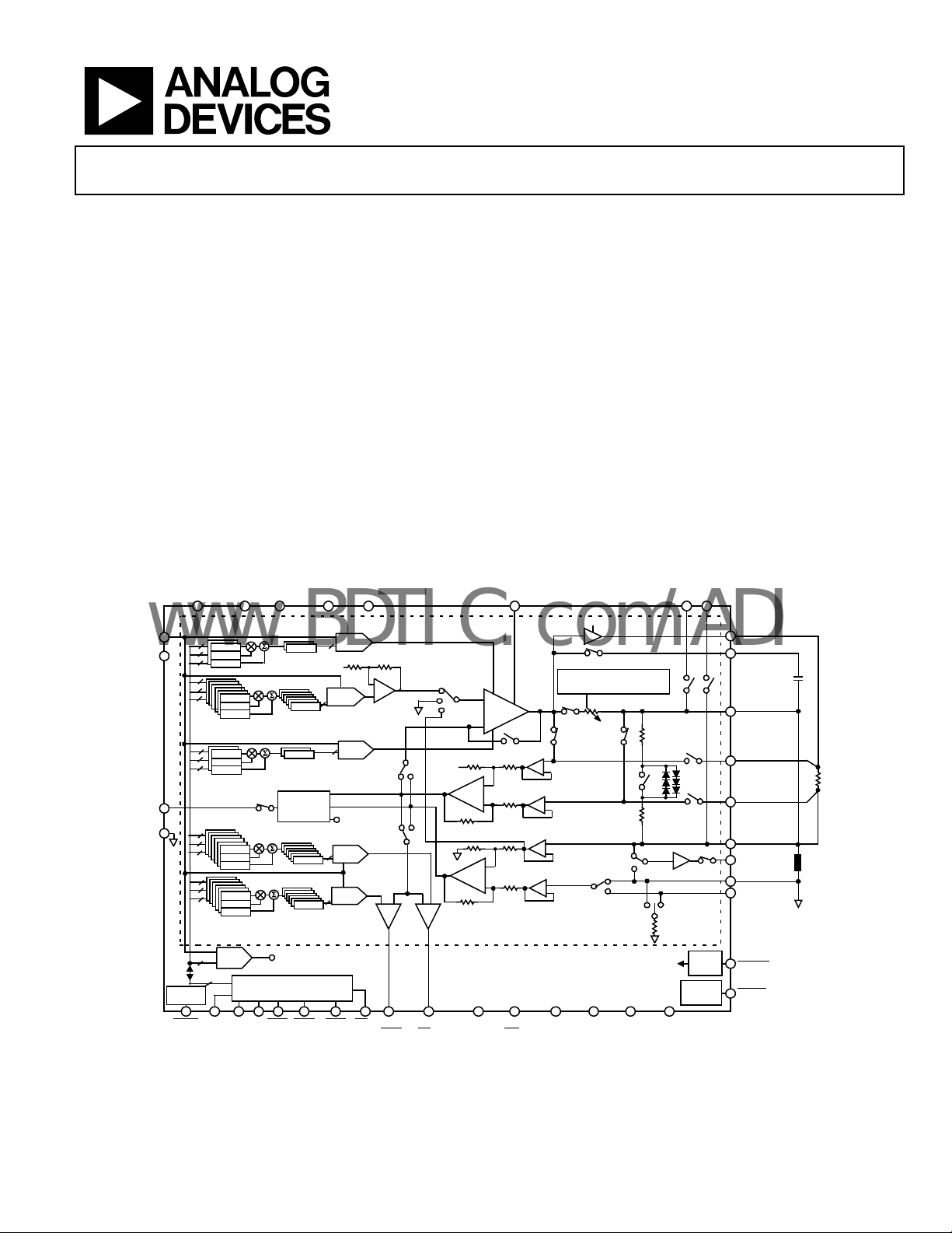
FUNCTIONAL BLOCK DIAGRAM
DGND
CPL
–
+
SW10
SW11
–
SCLK
+
AGND
×4
FIN
CPH
CPOH0/
SDI
–
16-BIT
CLH DAC
16-BIT
FIN DAC
16-BIT
16
CLL DAC
TEMP
SENSOR
16-BIT
CPH DAC
16-BIT
CPL DAC
COMPARATOR
SPI/
LVDS
Integrated 16-Bit Level Setting DACs
AD5522
APPLICATIONS
Automated test equipment (ATE)
Per-pin parametric measurement unit
Continuity and leakage testing
Device power supply
SENSE
VMIDTO
CENTER
I RANGE
+
)
SW1
MEASVH
(Hi-Z)
×5 or ×10
AGND
CPOL1/
SYNC
Figure 1.
Instrumentation
CCOMP[0:3]
CLH
+
FORCE
AMPLIFIER
–
SW2
CLL
+
–
MEASURE
CURRENT
IN-AMP
+
×1
–
MEASURE
VOLTAGE
IN-AMP
CPOH1/
SDO
Source measure unit (SMU)
Precision measurement
SYS_FORCE
EN
SW3
INTERNA L RANG E SELECT
(±5µA, ±20µA, ±200µ A, ±2m A)
SW5
R
SENSE
SW6
SW4
+
–
+
–
+
–
DUTGND
+
–
CPOL2/
CPO0
CPOH2/
CPO1
SW13
SW14
CPOL3/
CPO2
2kΩ
AGND
4kΩ
SW7
4kΩ
GUARDAMP
10kΩ
TO
MEASOU T
MUX
CPOH3/
CPO3
60Ω
SW15
SW8
SW9
CLAMPAND
GUARD
ALARM
SYS_SENSE
1kΩ
SW16
TEMP
SENSOR
EXTFOH[0:3]
CFF[0:3]
FOH[0:3]
EXTMEASIH[0:3]
EXTMEASIL[0:3]
MEASVH[0:3]
GUARD[0:3]
GUARDIN[0:3]/
DUTGND[0:3]
DUTGND
TMPALM
CGALM
EXTERNAL
R
(CURRENTS
UP TO ±80mA)
DUT
SENSE
06197-001
Rev.
A
Info
rmation furnished by Analog Devices is believed to be accurate and reliable. However, no
res
ponsibility is assumed by Analog Devices for its use, nor for any infringements of patents or other
righ
ts of third parties that may result from its use. Specifications subject to change without notice. No
license is granted by implication or otherwise under any patent or patent rights of Analog Devices.
Trademarks and registered trademarks are the property of their respective owners.
One Technology Way, P.O. Box 9106, Norwood, MA 02062-9106, U.S
Tel: 781.329.4700 www.analog.com
Fax: 781.461.3113 ©2008 Analog Devices, Inc. All rights reserved.
.A.
Page 2

AD5522
www.BDTIC.com/ADI
TABLE OF CONTENTS
Features .............................................................................................. 1
Applications ....................................................................................... 1
Functional Block Diagram .............................................................. 1
Revision History ............................................................................... 3
General Description ......................................................................... 4
Specifications ..................................................................................... 6
Timing Characteristics .............................................................. 11
Absolute Maximum Ratings .......................................................... 15
Thermal Resistance .................................................................... 15
ESD Caution ................................................................................ 15
Pin Configurations and Function Descriptions ......................... 16
Typical Performance Characteristics ........................................... 22
Terminology .................................................................................... 28
Theory of Operation ...................................................................... 29
Force Amplifier ........................................................................... 29
Comparators ................................................................................ 29
Clamps ......................................................................................... 29
Current Range Selection ............................................................ 30
High Current Ranges ................................................................. 30
Measure Current Gains .............................................................. 31
VMID Voltage ............................................................................. 31
Choosing Power Supply Rails ................................................... 32
Measure Output (MEASOUTx Pins) ...................................... 32
Device Under Test Ground (DUTGND) ................................. 32
Guard Amplifier ......................................................................... 33
Compensation Capacitors ......................................................... 33
System Force and Sense Switches ............................................. 33
Temperature Sensor ................................................................... 33
DAC Levels ...................................................................................... 34
Offset DAC .................................................................................. 34
Gain and Offset Registers .......................................................... 34
Cached X2 Registers ................................................................... 35
Reference Voltage (VREF) ......................................................... 35
Reference Selection .................................................................... 35
Calibration ................................................................................... 36
System Level Calibration ........................................................... 37
Circuit Operation ........................................................................... 38
Force Voltage (FV) Mode .......................................................... 38
Force Current (FI) Mode ........................................................... 39
Serial Interface ................................................................................ 40
SPI Interface ................................................................................ 40
LVDS Interface ............................................................................ 40
Serial Interface Write Mode ...................................................... 40
RESET
Function ......................................................................... 40
and
LOAD
Functions ..................................................... 40
BUSY
Register Update Rates ................................................................ 41
Register Selection ....................................................................... 41
Write System Control Register ................................................. 43
Write PMU Register ................................................................... 45
Write DAC Register ................................................................... 47
Read Registers ............................................................................. 50
Readback of System Control Register ...................................... 51
Readback of PMU Register ....................................................... 52
Readback of Comparator Status Register ................................ 53
Readback of Alarm Status Register .......................................... 53
Readback of DAC Register ........................................................ 54
Applications Information .............................................................. 55
Power-On Default ...................................................................... 55
Setting Up the Device on Power-On ....................................... 55
Changing Modes ........................................................................ 56
Required External Components ............................................... 56
Power Supply Decoupling ......................................................... 57
Power Supply Sequencing ......................................................... 57
Typical Application for the AD5522 ........................................ 57
Outline Dimensions ....................................................................... 59
Ordering Guide .......................................................................... 60
Rev. A | Page 2 of 60
Page 3

AD5522
www.BDTIC.com/ADI
REVISION HISTORY
10/08—Rev. 0 to Rev. A
Changes to Table 1 ............................................................................ 6
Change to 4 DAC X1 Parameter, Table 2 ..................................... 11
Changes to Table 3 .......................................................................... 12
Change to Reflow Soldering Parameter, Table 4 ......................... 15
Changes to Figure 18, Figure 19, Figure 20, and Figure 21 ....... 23
Changes to Figure 25 ...................................................................... 24
Changes to Force Amplifier Section ............................................. 29
Changes to Clamps Section ........................................................... 29
Changes to High Current Ranges Section ................................... 30
Changes to Choosing Power Supply Rails Section ..................... 32
Changes to Compensation Capacitors Section ........................... 33
Added Table 14, Renumbered Tables Sequentially ..................... 36
Changes to Reference Selection Example .................................... 36
Changes to Table 15 and
Section .............................................................................................. 40
Changes to Table 17 and Register Update Rates Section ........... 41
Added Table 38 ................................................................................ 57
Changes to Ordering Guide ........................................................... 60
7/08—Revision 0: Initial Version
BUSY
and
LOAD
Functions
Rev. A | Page 3 of 60
Page 4

AD5522
www.BDTIC.com/ADI
GENERAL DESCRIPTION
The AD5522 is a high performance, highly integrated parametric
measurement unit consisting of four independent channels. Each
per-pin parametric measurement unit (PPMU) channel includes
five 16-bit, voltage output DACs that set the programmable input
levels for the force voltage inputs, clamp inputs, and comparator
inputs (high and low). Five programmable force and measure
current ranges are available, ranging from ±5 µA to ±80 mA.
Four of these ranges use on-chip sense resistors; one high current
range up to ±80 mA is available per channel using off-chip sense
resistors. Currents in excess of ±80 mA require an external amplifier. Low capacitance DUT connections (FOH and EXTFOH)
ensure that the device is suited to relayless test systems.
The PMU functions are controlled via a simple 3-wire serial
interface compatible with SPI, QSPI™, MICROWIRE™, and DSP
interface standards. Interface clocks of 50 MHz allow fast updating
of modes. The low voltage differential signaling (LVDS) interface
protocol at 83 MHz is also supported. Comparator outputs are
provided per channel for device go-no-go testing and characterization. Control registers allow the user to easily change force or
measure conditions, DAC levels, and selected current ranges.
The SDO (serial data output) pin allows the user to read back
information for diagnostic purposes.
Rev. A | Page 4 of 60
Page 5
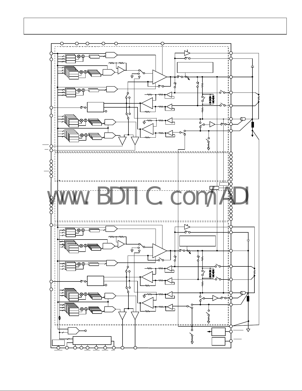
AD5522
K
www.BDTIC.com/ADI
VREF
REFGND
MEASOUT0
AGND
CPOL0/SCL
CPOH0/SDI
CCOMP1
MEASOUT1
CPOL1/SYNC
CPOH1/SDO
AGND
CCOMP2
MEASOUT2
CPOL2/CPO0
CPOH2/CPO1
AGND
CCOMP3
MEASOUT3
AGND
AGND
POWER-ON
RESET
AVSS AVDD
16
X1 REG
16
M REG
16
C REG
16
16
16
16
16
16
16
16
16
16
16
16
16
16
16
16
16
16
16
16
16
16
16
16
16
16
16
×2
X1 REG
M REG
C REG
×6
X1 REG
M REG
C REG
×2
SW12
×6
X1 REG
M REG
C REG
×6
X1 REG
M REG
C REG
X1 REG
M REG
C REG
×2
X1 REG
M REG
C REG
×6
X1 REG
M REG
C REG
×2
SW12
×6
X1 REG
M REG
C REG
×6
X1 REG
M REG
C REG
16-BIT
16
OFFSET
DAC
16
SDI
SCLK SYNC
SDORESET BUSY LOAD
X2 REG
X2 REG
X2 REG
MEASOU T
MUX AND GAI N
×1/×0.2
X2 REG
X2 REG
X2 REG
X2 REG
X2 REG
MEASOU T
MUX AND GAI N
x1/x0.2
X2 REG
X2 REG
TO ALL DAC
OUTPUT
AMPLIFIERS
SERIAL
INTERFACE
DVCC
16
×2
OFFSET DAC
×6
16
FIN DAC
16
×2
×6
16
×6
16
COMPARATOR
16
×2
OFFSET DAC
×6
16
FIN DAC
16
×2
×6
16
×6
16
DGND
16-BIT
CLH DAC
16-BIT
16-BIT
CLL DAC
TEMP
SENSOR
16-BIT
CPH DAC
16-BIT
CPL DAC
16-BIT
CLH DAC
16-BIT
16-BIT
CLL DAC
TEMP
SENSOR
16-BIT
CPH DAC
16-BIT
CPL DAC
COMPARATOR
SPI/
LVDS
CH0
–
CPL
FIN
+
AGND
SW10
SW11
–
+
CPH
–
VMID TO
CENTER
I RANGE
+
SW1
MEASVH
(Hi-Z)
×5 OR ×10
AGND
CLL
×1
CH1
CH2
CH3
–
CPL
+
SW10
SW11
–
CPOL3/
CPO2
FIN
AGND
+
SW1
MEASVH
(Hi-Z)
CLL
VMID TO
CENTER
I RANGE
x5 or x10
AGND
CPH
–
CPOH3/
CPO3
x1
+
Figure 2. Detailed Block Diagram
CLH
+
FORCE
AMPLIFIER
–
+
–
+
–
CLH
+
FORCE
AMPLIFIER
–
+
–
+
–
CCOMP0
MEASURE
CURRENT
IN-AMP
MEASURE
VOLTAGE
IN-AMP
MEASURE
CURRENT
IN-AMP
MEASURE
VOLTAGE
IN-AMP
(±5µA, ±20µA, ±200µ A, ±2m A)
SW5
SW2
SW4
+
–
+
–
+
–
DUTGND
+
–
SW2
SW4
+
–
+
–
+
–
DUTGND
+
–
EN
SW3
INTERNAL RANGE
SELECT
R
SENSE
SW6
4kΩ
2kΩ
SW7
4kΩ
SW13
SW3
SELECT
SW6
SW13
SW14
2kΩ
MEASOUT
MUX
10kΩ
AGND
4kΩ
SW7
4kΩ
AGND
TO
GUARD AMP
SW15
10kΩ
GUARD AMP
SW15
10kΩ
SW14
EN
INTERNAL RANGE
(±5µA, ±20µA, ±200µ A, ±2m A)
SW5
R
SENSE
SW15a
AGND
SW16
MUX
SW8
SW9
TEMP
SENSOR
CLAMP AND
GUARD
ALARM
SW8
SW9
MUX
SW16
EXTFOH0
CFF0
FOH0
EXTMEASIH0
EXTMEASIL0
MEASVH0
GUARD0
GUARDIN0/
DUTGND0
EXTFOH1
CFF1
FOH1
EXTMEASIH1
EXTMEASIL1
MEASVH1
GUARD1
GUARDIN1/DUTGND1
SYS_SENSE
SYS_FORCE
EXTFOH2
CFF2
FOH2
EXTMEASIH2
EXTMEASIL2
MEASVH2
GUARD2
GUARDIN2/DUTGND2
EXTFOH3
CFF3
FOH3
EXTMEASIH3
EXTMEASIL3
MEASVH3
GUARD3
GUARDIN3/
DUTGND3
DUT
DUTGND
TMPALM
CGALM
EXTERNAL
R
SENSE
(CURRENTS
UP TO ±80mA)
DUT
DUTGND
EXTERNAL
R
SENSE
(CURRENTS
UP TO ±80mA)
06197-002
Rev. A | Page 5 of 60
Page 6

AD5522
www.BDTIC.com/ADI
SPECIFICATIONS
AVDD ≥ 10 V; AVSS ≤ −5 V; |AVDD − AVSS| ≥ 20 V and ≤ 33 V; DVCC = 2.3 V to 5.25 V; VREF = 5 V; REFGND = DUTGND = AGND
= 0 V; gain (M), offset (C), and DAC offset registers at default values; T
FI = force current, MV = measure voltage, MI = measure current, FS = full scale, FSR = full-scale range, FSVR = full-scale voltage range,
FSCR = full-scale current range.)
Table 1.
Parameter Min Typ1 Max Unit Test Conditions/Comments
FORCE VOLTAGE
FOHx Output Voltage Range2 AVSS + 4 AVDD − 4 V All current ranges from FOHx at full-scale current;
EXTFOHx Output Voltage
Output Voltage Span 22.5 V
Offset Error −50 +50 mV Measured at midscale code; prior to calibration
Offset Error Tempco2 −10 µV/°C Standard deviation = 20 V/°C
Gain Error −0.5 +0.5 % FSR Prior to calibration
Gain Error Tempco2 0.5 ppm/°C Standard deviation = 0.5 ppm/°C
Linearity Error −0.01 +0.01 % FSR FSR = full-scale range (±10 V), gain and offset errors
Short-Circuit Current Limit2 −150 +150 mA ±80 mA range
−10 +10 mA All other ranges
Noise Spectral Density (NSD)2 320 nV/√Hz 1 kHz, at FOHx in FV mode
MEASURE CURRENT Measure current = (I
Differential Input Voltage
Range
Output Voltage Span 22.5 V Measure current block with VREF = 5 V, MEASOUT
Offset Error −0.5 +0.5 % FSCR V(R
Offset Error Tempco2 1 µV/°C Referred to MI input; standard deviation = 4 µV/°C
Gain Error −1 +1 % FSCR Using internal current ranges
−0.5 +0.5 % FSCR Measure current amplifier alone
Gain Error Tempco2 −2 ppm/°C Standard deviation = 2 ppm/°C
Linearity Error −0.015 +0.015 % FSCR Gain and offset errors calibrated out; MEASOUTx
−0.01 +0.01 % FSCR Gain and offset errors calibrated out; MEASOUTx
Common-Mode Voltage Range2 AVSS + 4 AVDD − 4 V
Common-Mode Error −0.005 +0.005 % FSVR/V % of full-scale change at measure output per V
Sense Resistors Sense resistors are trimmed to within 1%
200 kΩ ±5 µA range
50 kΩ ±20 µA range
5 kΩ ±200 µA range
0.5 kΩ ±2 mA range
Measure Current Ranges2 Specified current ranges are achieved with VREF = 5 V
±5 µA Set using internal sense resistor
±20 µA Set using internal sense resistor
±200 µA Set using internal sense resistor
±2 mA Set using internal sense resistor
±80 mA Set using external sense resistor; internal amplifier
Noise Spectral Density (NSD)2 400 nV/√Hz 1 kHz, MI amplifier only, inputs grounded
Range
2
2
AVSS + 3 AVDD − 3 V External high current range at full-scale current;
−1.125 +1.125 V Voltage across R
= 25°C to 90°C, unless otherwise noted. (FV = force voltage,
J
includes ±1 V dropped across sense resistor
does not include ±1 V dropped across sense resistor
calibrated out
× R
gain = 5 or 10, unless otherwise noted
scaling happens after
) = ±1 V, measured with zero current flowing
SENSE
gain = 1; MI gain = 10
gain = 1; MI gain = 5
change in DUT voltage
and MI gain = 10, or with VREF = 2.5 V and MI gain = 5
can drive up to ±80 mA
DUT
; gain = 5 or 10
SENSE
× gain); amplifier
SENSE
Rev. A | Page 6 of 60
Page 7

AD5522
www.BDTIC.com/ADI
Parameter Min Typ1Max Unit Test Conditions/Comments
FORCE CURRENT
Voltage Compliance, FOHx
Voltage Compliance, EXTFOHx
Offset Error −0.5 +0.5 % FSCR Measured at midscale code, 0 V, prior to calibration
Offset Error Tempco
Gain Error −1.5 +1.5 % FSCR Prior to calibration
Gain Error Tempco
Linearity Error −0.02 +0.02 % FSCR
Force Current Ranges Specified current ranges achieved with VREF = 5 V and
±5 µA Set using internal sense resistor, 200 kΩ
±20 µA Set using internal sense resistor, 50 kΩ
±200 µA Set using internal sense resistor, 5 kΩ
±2 mA Set using internal sense resistor, 500 Ω
±80 mA Set using external sense resistor; internal amplifier
MEASURE VOLTAGE
Measure Voltage Range
Offset Error −10 +10 mV Gain = 1, measured at 0 V
−25 +25 mV Gain = 0.2, measured at 0 V
Offset Error Tempco
Gain Error −0.25 +0.25 % FSR MEASOUTx gain = 1
−0.5 +0.5 % FSR MEASOUTx gain = 0.2
Gain Error Tempco
Linearity Error −0.01 +0.01 % FSR Gain = 1
Noise Spectral Density (NSD)
OFFSET DAC
Span Error ±30 mV
COMPARATOR
Comparator Span 22.5 V
Offset Error −2 +1 +2 mV Measured directly at comparator; does not include
Offset Error Tempco
Propagation Delay
VOLTAGE CLAMPS
Clamp Span 22.5 V
Positive Clamp Accuracy 155 mV
Negative Clamp Accuracy −155 mV
CLL to CLH
Recovery Time
Activation Time
2
2
2
CURRENT CLAMPS
Clamp Accuracy Programmed
Programmed
2
CLL to CLH
10 % of
Recovery Time
Activation Time
2
0.5 1.5 s
2
2
AVSS + 4 AVDD − 4 V
2
AVSS + 3 AVDD − 3 V
2
5 ppm
Standard deviation = 5 ppm/°C
FS/°C
2
−6 ppm/°C Standard deviation = 5 ppm/°C
MI gain = 10, or with VREF = 2.5 V and MI gain = 5 V
can drive up to ±80 mA
2
AVSS + 4 AVDD − 4 V
2
−1 µV/°C Standard deviation = 6 µV /°C
2
1 ppm/°C Standard deviation = 4 ppm/°C
2
100 nV/√Hz 1 kHz; measure voltage amplifier only, inputs
grounded
measure block errors
2
1 µV/°C Standard deviation = 2 µV/°C
2
0.25 s
500 mV CLL < CLH and minimum voltage apart
0.5 1.5 s
1.5 3 s
clamp value
clamp value + 10
Programmed
Programmed
clamp value
clamp value + 20
5 % of
% FSCR MI gain = 10, clamp current scales with selected
range
% FSCR MI gain = 5, clamp current scales with selected range
CLL < CLH and minimum setting apart, MI gain = 10
I
RANGE
CLL < CLH and minimum setting apart, MI gain = 5
I
RANGE
1.5 3 s
Rev. A | Page 7 of 60
Page 8

AD5522
www.BDTIC.com/ADI
Parameter Min Typ1Max Unit Test Conditions/Comments
FOHx, EXTFOHx, EXTMEASILx,
EXTMEASIHx, CFFx PINS
Pin Capacitance
2
10 pF
Leakage Current −3 +3 nA Individual pin on or off switch leakage, measured with
2
Leakage Current Tempco
MEASVHx PIN
Pin Capacitance
2
3 pF
Leakage Current −3 +3 nA Measured with ±11V stress applied to pin, channel
Leakage Current Tempco
2
±0.01 nA/°C
SYS_SENSE PIN SYS_SENSE connected, force amplifier inhibited
Pin Capacitance
2
3 pF
Switch Impedance 1 1.3 kΩ
Leakage Current −3 +3 nA Measured with ±11 V stress applied to pin, switch off
Leakage Current Tempco
2
±0.01 nA/°C
SYS_FORCE PIN SYS_FORCE connected, force amplifier inhibited
Pin Capacitance
2
6 pF
Switch Impedance 60 80 Ω
Leakage Current −3 +3 nA Measured with ±11 V stress applied to pin, switch off
Leakage Current Tempco
2
±0.01 nA/°C
COMBINED LEAKAGE AT DUT Includes FOHx, MEASVHx, SYS_SENSE, SYS_FORCE,
Leakage Current −15 +15 nA TJ = 25°C to 70°C
−25 +25 nA TJ = 25°C to 90°C
Leakage Current Tempco
2
±0.1 nA/°C
DUTGND PIN
Voltage Range −500 +500 mV
Leakage Current −30 +30 nA
MEASOUTx PIN With respect to AGND
Output Voltage Span 22.5 V Software programmable output range
Output Impedance 60 80 Ω
Output Leakage Current −3 +3 nA With SW12 off
2
Output Capacitance
Maximum Load Capacitance
2
Output Current Drive
Short-Circuit Current −10 +10 mA
Slew Rate
Enable Time
Disable Time
MI to MV Switching Time
2
2 V/s
2
150 320 ns
2
2
GUARDx PIN
Output Voltage Span 22.5 V
Output Offset −10 +10 mV
Short-Circuit Current −15 +15 mA
Maximum Load Capacitance
Output Impedance 85 Ω
Tristate Leakage Current
2
Slew Rate
Alarm Activation Time
2
2
±11 V stress applied to pin, channel enabled, but
tristate
±0.01 nA/°C
enabled, but tristate
EXTMEASILx, EXTMEASIHx, EXTFOHx, and CFFx;
calculation of all the individual leakage contributors
15 pF
2
0.5 F
2 mA
Closing SW12, measured from
400 1100 ns
200 ns
Opening SW12, measured from
Measured from
BUSY
rising edge; does not include
slewing or settling
2
100 nF
−30 +30 nA When guard amplifier is disabled
5 V/s C
LOAD
= 10 pF
200 s Alarm delayed to eliminate false alarms
BUSY
BUSY
rising edge
rising edge
Rev. A | Page 8 of 60
Page 9

AD5522
www.BDTIC.com/ADI
Parameter Min Typ1 Max Unit Test Conditions/Comments
FORCE AMPLIFIER2
Slew Rate 0.4 V/s CCOMPx = 100 pF, CFFx = 220 pF, C
Gain Bandwidth 1.3 MHz CCOMPx = 100 pF, CFFx = 220 pF, C
Max Stable Load Capacitance 10,000 pF CCOMPx = 100 pF, larger C
requires larger
LOAD
CCOMP
100 nF CCOMPx = 1 nF, larger C
FV SETTLING TIME TO 0.05% OF FS2
Midscale to full-scale change; measured from
requires larger CCOMP
LOAD
rising edge, clamps on
±80 mA Range 22 40 µs CCOMPx = 100 pF, CFFx = 220 pF, C
±2 mA Range 24 40 µs CCOMPx = 100 pF, CFFx = 220 pF, C
±200 µA Range 40 80 µs CCOMPx = 100 pF, CFFx = 220 pF, C
±20 µA Range 300 µs CCOMPx = 100 pF, CFFx = 220 pF, C
±5 µA Range 1400 µs CCOMPx = 100 pF, CFFx = 220 pF, C
MI SETTLING TIME TO 0.05% OF FS2 Midscale to full-scale change; driven from force
amplifier in FV mode, so includes FV settling time;
SYNC
measured from
rising edge, clamps on
±80 mA Range 22 40 µs CCOMPx = 100 pF, CFFx = 220 pF, C
±2 mA Range 24 40 µs CCOMPx = 100 pF, CFFx = 220 pF, C
±200 µA Range 60 100 µs CCOMPx = 100 pF, CFFx = 220 pF, C
±20 µA Range 462 µs CCOMPx = 100 pF, CFFx = 220 pF, C
±5 µA Range 1902 µs CCOMPx = 100 pF, CFFx = 220 pF, C
FI SETTLING TIME TO 0.05% OF FS2
Midscale to full-scale change; measured from
rising edge, clamps on
±80 mA Range 24 55 µs CCOMPx = 100 pF, C
±2 mA Range 24 60 µs CCOMPx = 100 pF, C
±200 µA Range 50 120 µs CCOMPx = 100 pF, C
±20 µA Range 450 µs CCOMPx = 100 pF, C
±5 µA Range 2700 µs CCOMPx = 100 pF, C
= 200 pF
LOAD
= 200 pF
LOAD
= 200 pF
LOAD
= 200 pF
LOAD
= 200 pF
LOAD
MV SETTLING TIME TO 0.05% OF FS2 Midscale to full-scale change; driven from force
amplifier in FV mode, so includes FV settling time;
SYNC
measured from
±80 mA Range 24 55 µs CCOMPx = 100 pF, C
±2 mA Range 24 60 µs CCOMPx = 100 pF, C
±200 µA Range 50 120 µs CCOMPx = 100 pF, C
±20 µA Range 450 µs CCOMPx = 100 pF, C
±5 µA Range 2700 µs CCOMPx = 100 pF, C
rising edge, clamps on
= 200 pF
LOAD
= 200 pF
LOAD
= 200 pF
LOAD
= 200 pF
LOAD
= 200 pF
LOAD
DAC SPECIFICATIONS
Resolution 16 Bits
Output Voltage Span2 22.5 V VREF = 5 V, within a range of −16.25 V to +22.5 V
Differential Nonlinearity2 −1 +1 LSB Guaranteed monotonic by design over temperature
COMPARATOR DAC DYNAMIC
SPECIFICATIONS
2
Output Voltage Settling Time 1 µs 500 mV change to ±½ LSB
Slew Rate 5.5 V/µs
Digital-to-Analog Glitch Energy 20 nV-s
Glitch Impulse Peak Amplitude 10 mV
REFERENCE INPUT
VREF DC Input Impedance 1 100 MΩ
VREF Input Current −10 +0.03 +10 µA
VREF Range2 2 5 V
DIE TEMPERATURE SENSOR
Accuracy2 ±7 °C
Output Voltage at 25°C 1.5 V
Output Scale Factor2 4.6 mV/°C
Output Voltage Range2 0 3 V
= 200 pF
LOAD
= 200 pF
LOAD
= 200 pF
LOAD
= 200 pF
LOAD
= 200 pF
LOAD
= 200 pF
LOAD
= 200 pF
LOAD
= 200 pF
LOAD
= 200 pF
LOAD
= 200 pF
LOAD
= 200 pF
LOAD
= 200 pF
LOAD
SYNC
SYNC
Rev. A | Page 9 of 60
Page 10

AD5522
www.BDTIC.com/ADI
Parameter Min Typ1Max Unit Test Conditions/Comments
INTERACTION AND CROSSTALK
DC Crosstalk (FOHx) 0.05 0.65 mV DC change resulting from a dc change in any DAC
DC Crosstalk (MEASOUTx) 0.05 0.65 mV DC change resulting from a dc change in any DAC
DC Crosstalk Within a Channel 0.05 mV All channels in FVMI mode, one channel at
SPI INTERFACE LOGIC INPUTS
Input High Voltage, VIH 1.7/2.0 V (2.3 V to 2.7 V)/(2.7 V to 5.25 V), JEDEC-compliant
Input Low Voltage, VIL 0.7/0.8 V (2.3 V to 2.7 V)/(2.7 V to 5.25 V), JEDEC-compliant
Input Current, I
, I
INH
INL
Input Capacitance, C
CMOS LOGIC OUTPUTS SDO, CPOx
Output High Voltage, VOH DVCC − 0.4 V
Output Low Voltage, VOL 0.4 V IOL = 500 µA.
Tristate Leakage Current −2 +2 µA
−1 +1 µA All other output pins
Output Capacitance
2
OPEN-DRAIN LOGIC OUTPUTS
Output Low Voltage, VOL 0.4 V IOL = 500 µA, C
Output Capacitance
2
LVDS INTERFACE LOGIC INPUTS
REDUCED RANGE LINK
Input Voltage Range 875 1575 mV
Input Differential Threshold −100 +100 mV
External Termination Resistance 80 100 120 Ω
Differential Input Voltage 100 mV
LVDS INTERFACE LOGIC OUTPUTS
REDUCED RANGE LINK
Output Offset Voltage 1200 mV
Output Differential Voltage 400 mV
POWER SUPPLIES
AVDD 10 28 V |AVDD − AVSS| ≤ 33 V
AVSS −23 −5 V
DVCC 2.3 5.25 V
AIDD 26 mA Internal ranges (±5 A to ±2 mA), excluding load
AISS −26 mA Internal ranges (±5 A to ±2 mA), excluding load
AIDD 28 mA Internal ranges (±5 A to ±2 mA), excluding load
AISS −28 mA Internal ranges (±5 A to ±2 mA), excluding load
AIDD 36 mA External range, excluding load conditions
AISS −36 mA External range, excluding load conditions
DICC 1.5 mA
Maximum Power Dissipation
2
in the device, FV and FI modes, ±2 mA range, C
= 200 pF, R
LOAD
in the device, MV and MI modes, ±2 mA range,
= 200 pF, R
C
LOAD
midscale; measure the current for one channel in
the lowest current range for a change in
comparator or clamp DAC levels for that PMU
input levels
input levels
−1 +1 µA
2
10 pF
IN
SDO, CPOH1/
10 pF
BUSY
10 pF
2
SDO
TMPALM, CGALM
,
LOAD
conditions; comparators and guard disabled
conditions; comparators and guard disabled
conditions; comparators and guard enabled
conditions; comparators and guard enabled
2
7 W Maximum power that should be dissipated in this
package under worst-case load conditions; careful
consideration should be given to supply selection
and thermal design
= 5.6 kΩ
= 5.6 kΩ
LOAD
= 50 pF, R
LOAD
= 1 kΩ
PULLUP
Rev. A | Page 10 of 60
Page 11
AD5522
www.BDTIC.com/ADI
Parameter Min Typ1Max Unit Test Conditions/Comments
Power Supply Sensitivity
∆Forced Voltage/∆AVDD −80 dB
∆Forced Voltage/∆AVSS −80 dB
∆Measured Current/∆AVDD −85 dB
∆Measured Current/∆AVSS −75 dB
∆Forced Current/∆AVDD −75 dB
∆Forced Current/∆AVSS −75 dB
∆Measured Voltage/∆AVDD −85 dB
∆Measured Voltage/∆AVSS −80 dB
∆Forced Voltage/∆DVCC −90 dB
∆Measured Current/∆DVCC −90 dB
∆Forced Current/∆DVCC −90 dB
∆Measured Voltage/∆DVCC −90 dB
1
Typical specifications are at 25°C and nominal supply, ±15.25 V, unless otherwise noted.
2
Guaranteed by design and characterization; not production tested. Tempco values are mean and standard deviation, unless otherwise noted.
TIMING CHARACTERISTICS
AVDD ≥ 10 V, AVSS ≤ −5 V, |AVDD − AVSS| ≥ 20 V and ≤ 33 V, DVCC = 2.3 V to 5.25 V, VREF = 5 V, TJ = 25°C to 90°C, unless
otherwise noted.
Table 2. SPI Interface
1 , 2 , 3
Parameter
4
t
WRIT E
t
1
t2 8 8 8 ns min SCLK high time
t3 8 8 8 ns min SCLK low time
t4 10 10 10 ns min
4
t
150 150 150 ns min
5
t6 10 5 5 ns min
t
7
t8 9 7 4.5 ns min Data hold time
t9 120 75 55 ns max
t10
1 DAC X1 1.5 1.5 1.5 µs max
2 DAC X1 2.1 2.1 2.1 µs max
3 DAC X1 2.7 2.7 2.7 µs max
4 DAC X1 3.3 3.3 3.3 µs max
Other Registers 270 270 270 ns max System control register/PMU registers
t11 20 20 20 ns min
t12 20 20 20 ns min
t13 150 150 150 ns min
t14 0 0 0 ns min
t15 100 100 100 ns max
2
From dc to 1 kHz
DVCC, Limit at T
2.3 V to 2.7 V 2.7 V to 3.6 V 4.5 V to 5.25 V
MIN
, T
MAX
Unit Description
1030 735 735 ns min Single channel update cycle time (X1 register write)
950 655 655 ns min
Single channel update cycle time (any other register
write)
30 20 20 ns min SCLK cycle time
falling edge to SCLK falling edge setup time
SYNC
Minimum SYNC
high time in write mode after X1
register write (one channel)
70 70 70 ns min
Minimum SYNC
high time in write mode after any
other register write
th
SCLK falling edge to SYNC rising edge
29
5 5 5 ns min Data setup time
rising edge to BUSY falling edge
SYNC
pulse width low; see Table 17
BUSY
th
SCLK falling edge to LOAD falling edge
29
pulse width low
LOAD
rising edge to FOHx output response time
BUSY
rising edge to LOAD falling edge
BUSY
rising edge to FOHx output response time
LOAD
Rev. A | Page 11 of 60
Page 12

AD5522
www.BDTIC.com/ADI
Parameter
1 , 2 , 3
2.3 V to 2.7 V 2.7 V to 3.6 V 4.5 V to 5.25 V
t16 1.8 1.2 0.9 ns min
t17 670 700 750 µs max
t18 400 400 400 ns min
DVCC, Limit at T
5, 6
t
60 45 25 ns max SCLK rising edge to SDO valid; DVCC = 5 V to 5.25 V
19
1
Guaranteed by design and characterization; not production tested.
2
All input signals are specified with tR = tF = 2 ns (10% to 90% of DVCC) and timed from a voltage level of 1.2 V.
3
See Figure 5 and Figure 6.
4
Writes to more than one X1 register, engages the calibration engine for longer times, shown by the
should either be timed or should wait until
5
t19 is measured with the load circuit shown in Figure 4.
6
SDO output slows with lower DVCC supply and may require use of a slower SCLK.
BUSY
returns high (see Figure 53). This is required to ensure data is not lost or overwritten.
Table 3. LVDS Interface
DVCC, Limit at T
Parameter
1, 2, 3
2.7 V to 3.6 V 4.5 V to 5.25 V Unit Description
t1 20 12 ns min SCLK cycle time
t2 8 5 ns min SCLK pulse width high and low time
t3 3 3 ns min
t4 3 3 ns min Data setup time
t5 5 3 ns min Data hold time
t6 3 3 ns min
4
t
7
45 25 ns min SCLK rising edge to SDO valid
t8 150 150 ns min
70 70 ns min
400 400 ns min
1
Guaranteed by design and characterization; not production tested.
2
All input signals are specified with tR = tF = 2 ns (10% to 90% of DVCC) and timed from a voltage level of 1.2 V.
3
See Figure 7.
4
SDO output slows with lower DVCC supply and may require use of slower SCLK.
MIN
MIN
, T
MAX
Unit Description
RESET
RESET
Minimum SYNC
BUSY
low time, t10. Subsequent writes to one or more X1 registers
, T
MAX
SYNC
SCLK to SYNC
Minimum SYNC
register write
Minimum SYNC
other register write
Minimum SYNC
pulse width low
time indicated by BUSY low
high time in readback mode
to SCLK setup time
hold time
high time in write mode after X1
high time in write mode after any
high time in readback mode
Rev. A | Page 12 of 60
Page 13
AD5522
www.BDTIC.com/ADI
Circuit and Timing Diagrams
TO
OUTPUT
PIN
Figure 3. Load Circuit for
SCLK
SYNC
SDI
BUSY
C
DVCC
2.2kΩ
R
LOAD
V
50pF
LOAD
CGALM, TMPALM
11
2
t
4
t
7
DB28
OL
06197-003
t
1
29
t
3
t
8
t
2
t
6
t
5
DB0
t
9
TO OUTPUT
PIN
Figure 4. Load Circuit for SDO,
DB28
t
10
C
LOAD
50pF
200µA I
200µA I
OL
VOH(MIN) – VOL(MAX)
OH
BUSY
Timing Diagram
2
00406197-
29
DB0
LOAD
FOHx
LOAD
FOHx
RESET
BUSY
1
1
2
2
1
LOAD ACTIVE DURING BUSY.
2
LOAD ACTIVE AFTER BUSY.
t
11
t
16
t
17
t
12
t
13
t
14
t
12
t
15
06197-005
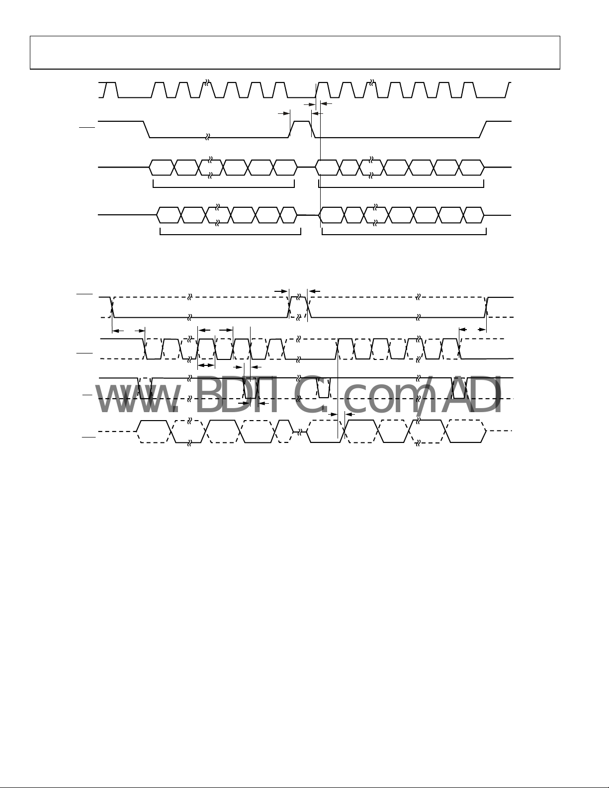
Figure 5. SPI Write Timing (Write Word Contains 29 Bits)
Rev. A | Page 13 of 60
Page 14
AD5522
www.BDTIC.com/ADI
SCLK
SYNC
29
t
t
18
19
58
SDI
SDO
INPUT WORD SPECIFIES
REGISTE R TO BE READ
UNDEFINED
DB23/
0BD82BD DB0
DB28
DB23/
DB28
NOP CONDITION
SELECTED REGISTER DATA
CLOCKED OUT
DB0
7-0060619
Figure 6. SPI Read Timing (Readback Word Contains 24 Bits and Can Be Clocked Out with a Minimum of 24 Clock Edges)
t
SYNC
SYNC
SCLK
SCLK
SDI
SDI
SDO
SDO
t
3
MSB
D28
t
1
t
2
UNDEFINED
LSB
D0
t
4
t
5
8
MSB
D23/D28
LSB
D0
t
7
MSB
DB23/
DB28
SELECTED REGISTER DAT A CLOCKED OUT
LSB
DB0
t
6
6197-007
Figure 7. LVDS Read and Write Timing (Readback Word Contains 24 Bits and Can Be Clocked Out with a Minimum of 24 Clock Edges)
Rev. A | Page 14 of 60
Page 15
AD5522
www.BDTIC.com/ADI
ABSOLUTE MAXIMUM RATINGS
Table 4.
Parameter
Supply Voltage, AVDD to AVSS 34 V
AVDD to AGND −0.3 V to +34 V
AVSS to AGND +0.3 V to −34 V
VREF to AGND −0.3 V to +7 V
DUTGND to AGND AVDD + 0.3 V to AVSS − 0.3 V
REFGND to AGND AVDD + 0.3 V to AVSS − 0.3 V
DVCC to DGND −0.3 V to +7 V
AGND to DGND −0.3 V to +0.3 V
Digital Inputs to DGND −0.3 V to DVCC + 0.3 V
Analog Inputs to AGND AVSS − 0.3 V to AVDD + 0.3 V
Storage Temperature Range −65°C to +125°C
Operating Junction Temperature
Range (J Version)
Reflow Soldering JEDEC Standard (J-STD-020)
Junction Temperature 150°C max
Rating
25°C to 90°C
Stresses above those listed under Absolute Maximum Ratings
may cause permanent damage to the device. This is a stress
rating only; functional operation of the device at these or any
other conditions above those indicated in the operational
section of this specification is not implied. Exposure to absolute
maximum rating conditions for extended periods may affect
device reliability.
THERMAL RESISTANCE
Thermal resistance values are specified for the worst-case
conditions, that is, a device soldered in a circuit board for
surface-mount packages.
1
Table 5. Thermal Resistance
Package Type
TQFP Exposed Pad Down 4.8 °C/W
No Heat Sink
200 17.2
500 15.1
With Cooling Plate at 45°C
TQFP Exposed Pad Up 2 °C/W
No Heat Sink
200 37.2
500 35.7
With Cooling Plate at 45°C3 N/A4 3.0 2 °C/W
1
The information in this section is based on simulated thermal information.
2
These values apply to the package with no heat sink attached. The actual
thermal performance of the package depends on the attached heat sink and
environmental conditions.
3
Natural convection at 55°C ambient. Assumes perfect thermal contact
between the cooling plate and the exposed paddle.
3
N/A means not applicable.
2
0 22.3 °C/W
2
0 42.4 °C/W
(JEDEC 4-Layer (1S2P) Board)
Airflow
(LFPM) θJA θJC
3
N/A 5.4 4.8 °C/W
Unit
°C/W
°C/W
°C/W
°C/W
ESD CAUTION
Rev. A | Page 15 of
60
Page 16

AD5522
www.BDTIC.com/ADI
PIN CONFIGURATIONS AND FUNCTION DESCRIPTIONS
EXTFOH162AVSS
EXTFOH0
80
1
AVDD
CFF0
CCOMP0
EXTMEASIH0
EXTMEASIL0
FOH0
GUARD0
GUARDIN0/DUTGND0
GUARDIN2/DUTGND2
NOTES:
1.
FOR PROPER CONNECTION OFTHE EXPOSED PAD, REFER T O THE PIN CONFIGURAT I ON AND FUNCTIO N DESCRIPT IONS SECTI ON OF THIS DATA SHEE T.
MEASVH0
AGND
AGND
MEASVH2
GUARD2
FOH2
EXTMEASIL2
EXTMEASIH2
CCOMP2
CFF2
AVDD
PIN 1
2
3
4
5
6
7
8
9
10
11
12
13
14
15
16
17
18
19
20
21
22
23
24
25
26
AVSS
SCLK
BUSY
EXTFOH2
CPOL0/SCLK
AD5522
TOP VIEW
EXPOSED PAD ON BOTTOM
(Not to S cale)
27
28
29
30
SDI
SYNC
DGND
CPOH0/SDI
CPOL1/SYNC
SYS_FORCE69AGND70SYS_SENSE71REFGND72VREF73DUTGND74AVDD75SPI/LVDS76CGALM77TMPALM78RESET79AVSS
68
31
32 33
CPOH1/SDO
35
SDO
LOAD34DVCC
CPOL2/CPO0
Figure 8. Pin Configuration, Exposed Pad on Bottom
MEASOUT364MEASOUT265MEASOUT166MEASOUT067AVSS
61
63
60
AVDD
59
CFF1
58
CCOMP1
57
EXTMEASIH1
56
EXTMEASIL1
55
FOH1
54
GUARD1
53
GUARDIN1/DUTGND1
52
MEASVH1
51
AGND
50
AGND
49
MEASVH3
48
GUARDIN3/DUTGND3
47
GUARD3
46
FOH3
45
EXTMEASIL3
44
EXTMEASIH3
43
CCOMP3
42
CFF3
41
AVDD
36
37
38
39
40
AVSS
EXTFOH3
CPOL3/CPO2
CPOH2/CPO1
CPOH3/CPO3
06197-008
Table 6. Pin Function Descriptions
Pin No. Mnemonic Description
Exposed pad
The exposed pad is internally electrically connected to AVSS. For enhanced thermal, electrical, and board level
performance, the exposed paddle on the bottom of the package should be soldered to a corresponding
thermal land paddle on the PCB.
1, 20, 41,
AVDD
Positive Analog Supply Voltage.
60, 74
2 CFF0
External Capacitor for Channel 0. This pin optimizes the stability and settling time performance of the force
amplifier when in force voltage mode. See the Compensation Capacitors section.
3 CCOMP0
4 EXTMEASIH0
5 EXTMEASIL0
6 FOH0
7 GUARD0
8
GUARDIN0/
DUTGND0
Compensation Capacitor Input for Channel 0. See the Compensation Capacitors section.
Sense Input (High Sense) for High Current Range (Channel 0).
Sense Input (Low Sense) for High Current Range (Channel 0).
Force Output for Internal Current Ranges (Channel 0).
Guard Output Drive for Channel 0.
Guard Amplifier Input for Channel 0/DUTGND Input for Channel 0. This dual function pin is configured via the
serial interface. The default function at power-on is GUARDIN0. If this pin is configured as a DUTGND input for
the channel, the input to the guard amplifier is internally connected to MEASVH0. For more information, see
the Device Under Test Ground (DUTGND) section and the Guard Amplifier section.
9 MEASVH0
10, 11, 50,
AGND
DUT Voltage Sense Input (High Sense) for Channel 0.
Analog Ground. These pins are the reference points for the analog supplies and the measure circuitry.
51, 69
12 MEASVH2 DUT Voltage Sense Input (High Sense) for Channel 2.
Rev. A | Page 16 of 60
Page 17

AD5522
www.BDTIC.com/ADI
Pin No. Mnemonic Description
13
14 GUARD2 Guard Output Drive for Channel 2.
15 FOH2 Force Output for Internal Current Ranges (Channel 2).
16 EXTMEASIL2 Sense Input (Low Sense) for High Current Range (Channel 2).
17 EXTMEASIH2 Sense Input (High Sense) for High Current Range (Channel 2).
18 CCOMP2 Compensation Capacitor Input for Channel 2. See the Compensation Capacitors section.
19 CFF2
21 EXTFOH2
22, 39, 62,
67, 79
23
24 SCLK
25
26
27 SDI Serial Data Input for SPI or LVDS Interface.
28
29 CPOL1/SYNC Comparator Output Low (Channel 1) for SPI Interface/Differential SYNC Input for LVDS Interface.
30 DGND Digital Ground Reference Point.
31
32 SDO Serial Data Output for SPI or LVDS Interface. This pin can be used for data readback and diagnostic purposes.
33
34 DVCC Digital Supply Voltage.
35 CPOL2/CPO0
36 CPOH2/CPO1
37 CPOL3/CPO2
38 CPOH3/CPO3
40 EXTFOH3
42 CFF3
43 CCOMP3 Compensation Capacitor Input for Channel 3. See the Compensation Capacitors section.
44 EXTMEASIH3 Sense Input (High Sense) for High Current Range (Channel 3).
45 EXTMEASIL3 Sense Input (Low Sense) for High Current Range (Channel 3).
46 FOH3 Force Output for Internal Current Ranges (Channel 3).
47 GUARD3 Guard Output Drive for Channel 3.
48
GUARDIN2/
DUTGND2
Guard Amplifier Input for Channel 2/DUTGND Input for Channel 2. This dual function pin is configured via the
serial interface. The default function at power-on is GUARDIN2. If this pin is configured as a DUTGND input for
the channel, the input to the guard amplifier is internally connected to MEASVH2. For more information, see
the Device Under Test Ground (DUTGND) section and the Guard Amplifier section.
External Capacitor for Channel 2. This pin optimizes the stability and settling time performance of the force
amplifier when in force voltage mode. See the Compensation Capacitors section.
Force Output for High Current Range (Channel 2). Use an external resistor at this pin for current ranges up to
±80 mA. For more information, see the Current Range Selection section.
AVSS Negative Analog Supply Voltage.
Digital Input/Open-Drain Output. This pin indicates the status of the interface. See the BUSY and LOAD
BUSY
Functions section for more information.
Serial Clock Input, Active Falling Edge. Data is clocked into the shift register on the falling edge of SCLK. This
pin operates at clock speeds up to 50 MHz.
CPOL0/SCLK
Comparator Output Low (Channel 0) for SPI Interface/Differential Serial Clock Input (Complement) for LVDS
Interface.
CPOH0/SDI
Comparator Output High (Channel 0) for SPI Interface/Differential Serial Data Input (Complement) for LVDS
Interface.
SYNC
CPOH1/SDO
Active Low Frame Synchronization Input for SPI or LVDS Interface.
Comparator Output High (Channel 1) for SPI Interface/Differential Serial Data Output (Complement) for LVDS
Interface.
Logic Input (Active Low). This pin synchronizes updates within one device or across a group of devices. If
LOAD
synchronization is not required, LOAD
can be tied low; in this case, DAC channels and PMU modes are updated
immediately after BUSY goes high. See the BUSY and LOA D Functions section for more information.
Comparator Output Low (Channel 2) for SPI Interface/Comparator Output Window (Channel 0) for LVDS
Interface.
Comparator Output High (Channel 2) for SPI Interface/Comparator Output Window (Channel 1) for LVDS
Interface.
Comparator Output Low (Channel 3) for SPI Interface/Comparator Output Window (Channel 2) for LVDS
Interface.
Comparator Output High (Channel 3) for SPI Interface/Comparator Output Window (Channel 3) for LVDS
Interface.
Force Output for High Current Range (Channel 3). Use an external resistor at this pin for current ranges up to
±80 mA. For more information, see the Current Range Selection section.
External Capacitor for Channel 3. This pin optimizes the stability and settling time performance of the force
amplifier when in force voltage mode. See the Compensation Capacitors section.
GUARDIN3/
DUTGND3
Guard Amplifier Input for Channel 3/DUTGND Input for Channel 3. This dual function pin is configured via the
serial interface. The default function at power-on is GUARDIN3. If this pin is configured as a DUTGND input for
the channel, the input to the guard amplifier is internally connected to MEASVH3. For more information, see
the Device Under Test Ground (DUTGND) section and the Guard Amplifier section.
Rev. A | Page 17 of 60
Page 18

AD5522
www.BDTIC.com/ADI
Pin No. Mnemonic Description
49 MEASVH3 DUT Voltage Sense Input (High Sense) for Channel 3.
52 MEASVH1 DUT Voltage Sense Input (High Sense) for Channel 1.
53
54 GUARD1 Guard Output Drive for Channel 1.
55 FOH1 Force Output for Internal Current Ranges (Channel 1).
56 EXTMEASIL1 Sense Input (Low Sense) for High Current Range (Channel 1).
57 EXTMEASIH1 Sense Input (High Sense) for High Current Range (Channel 1).
58 CCOMP1 Compensation Capacitor Input for Channel 1. See the Compensation Capacitors section.
59 CFF1
61 EXTFOH1
63 MEASOUT3
64 MEASOUT2
65 MEASOUT1
66 MEASOUT0
68 SYS_FORCE External Force Signal Input. This pin enables the connection of the system PMU.
70 SYS_SENSE External Sense Signal Output. This pin enables the connection of the system PMU.
71 REFGND Accurate Analog Reference Input Ground.
72 VREF Reference Input for DAC Channels (5 V for specified performance).
73 DUTGND
75
76
77
78
80 EXTFOH0
GUARDIN1/
DUTGND1
/LVDS Interface Select Pin. Logic low selects SPI-compatible interface mode; logic high selects LVDS interface mode.
SPI
Open-Drain Output for Guard and Clamp Alarms. This open-drain pin provides shared alarm information
CGALM
TMPALM
Digital Reset Input. This active low, level sensitive input resets all internal nodes on the device to their power-
RESET
Guard Amplifier Input for Channel 1/DUTGND Input for Channel 1. This dual function pin is configured via the
serial interface. The default function at power-on is GUARDIN1. If this pin is configured as a DUTGND input for
the channel, the input to the guard amplifier is internally connected to MEASVH1. For more information, see
the Device Under Test Ground (DUTGND) section and the Guard Amplifier section.
External Capacitor for Channel 1. This pin optimizes the stability and settling time performance of the force
amplifier when in force voltage mode. See the Compensation Capacitors section.
Force Output for High Current Range (Channel 1). Use an external resistor at this pin for current ranges up to
±80 mA. For more information, see the Current Range Selection section.
Multiplexed DUT Voltage, Current Sense Output, Temperature Sensor Voltage for Channel 3. This pin is
referenced to AGND.
Multiplexed DUT Voltage, Current Sense Output, Temperature Sensor Voltage for Channel 2. This pin is
referenced to AGND.
Multiplexed DUT Voltage, Current Sense Output, Temperature Sensor Voltage for Channel 1. This pin is
referenced to AGND.
Multiplexed DUT Voltage, Current Sense Output, Temperature Sensor Voltage for Channel 0. This pin is
referenced to AGND.
DUT Voltage Sense Input (Low Sense). By default, this input is shared among all four PMU channels. If a DUTGND
input is required for each channel, the user can configure the GUARDINx/DUTGNDx pins as DUTGND inputs for
each PMU channel.
This pin has a pull-down current source (~350 A). In LVDS interface mode, the CPOHx and CPOLx pins default
to differential interface pins.
about the guard amplifier and clamp circuitry. By default, this output pin is disabled. The system control
register allows the user to enable this function and to set the open-drain output as a latched output. The user
can also choose to enable alarms for the guard amplifier, the clamp circuitry, or both. When this pin flags an
alarm, the origins of the alarm can be determined by reading back the alarm status register. Two flags per
channel in this word (one latched, one unlatched) indicate which function caused the alarm and whether the
alarm is still present.
Open-Drain Output for Temperature Alarm. This latched, active low, open-drain output flags a temperature
alarm to indicate that the junction temperature has exceeded the default temperature setting (130°C) or the
user programmed temperature setting. Two flags in the alarm status register (one latched, one unlatched)
indicate whether the temperature has dropped below 130°C or remains above 130°C. User action is required
to clear this latched alarm flag by writing to the clear bit (Bit 6) in any of the PMU registers.
on reset values.
Force Output for High Current Range (Channel 0). Use an external resistor at this pin for current ranges up to
±80 mA. For more information, see the Current Range Selection section.
Rev. A | Page 18 of 60
Page 19

AD5522
www.BDTIC.com/ADI
EXTFOH0
AVSS
RESET
TMPALM
CGALM
SPI/LVDS
AVDD
DUTGND
VREF
REFGND
SYS_SENSE
AGND
SYS_FORCE
AVSS
MEASOUT0
MEASOUT1
MEASOUT2
MEASOUT3
AVSS
EXTFOH1
AVDD2CFF03CCOMP04EXTMEASIH05EXTMEASIL06FOH07GUARD08GUARDIN0/DUTGND09MEASVH010AGND11AGND12MEASVH213GUARDIN2/DUTGND214GUARD215FOH216EXTMEASIL217EXTMEASIH218CCOMP219CFF220AVDD
80
1
PIN 1
76
77
78
79
73
74
75
70
71
72
66
67
68
69
AD5522
TOP VIEW
EXPOSED PAD ON TOP
(Not to Scale)
21
22
AVDD
23
24
CFF1
CCOMP1
27
25
26
28
FOH1
GUARD1
EXTMEASIL1
EXTMEASIH1
IN1/DUTGND1
31
29
30
32 33
AGND51AGND
MEASVH1
35
34
GUARD3
MEASVH3
IN3/DUTGND3GUARD
61
62
63
64
65
60
EXTFOH2
59
AVSS
58
BUSY
57
SCLK
56
CPOL0/SCLK
55
CPOH0/SDI
54
SDI
53
SYNC
52
CPOL1/SYNC
DGND
CPOH1/SDO
50
SDO
49
LOAD
48
DVCC
47
CPOL2/CPO0
46
45
CPOH2/CPO1
44
CPOL3/CPO2
43
CPOH3/CPO3
42
AVSS
41
EXTFOH3
36
37
38
39
40
FOH3
EXTMEASIL3
CFF3
AVDD
CCOMP3
EXTMEASIH3
06197-009
NOTES:
1.
FOR PROPER CONNECTION OFTHE EXPOSED PAD, REFER T O THE PIN CONFIGURAT ION AND FUNCTION DESCRIPTIONS S ECTION OF THIS DATA SHEET.
Table 7. Pin Function Descriptions
Pin No. Mnemonic Description
1 EXTFOH0
Exposed pad The exposed pad is electrically connected to AVSS.
Force Output for High Current Range (Channel 0). Use an external resistor at this pin for current ranges up to
±80 mA. For more information, see the Current Range Selection section.
2, 14, 19,
AVSS
Negative Analog Supply Voltage.
42, 59
3
Digital Reset Input. This active low, level sensitive input resets all internal nodes on the device to their power-
RESET
on reset values.
4
TMPALM
Open-Drain Output for Temperature Alarm. This latched, active low, open-drain output flags a temperature
alarm to indicate that the junction temperature has exceeded the default temperature setting (130°C) or the
user programmed temperature setting. Two flags in the alarm status register (one latched, one unlatched)
indicate whether the temperature has dropped below 130°C or remains above 130°C. User action is required
to clear this latched alarm flag by writing to the clear bit (Bit 6) in any of the PMU registers.
5
CGALM
Open-Drain Output for Guard and Clamp Alarms. This open-drain pin provides shared alarm information
about the guard amplifier and clamp circuitry. By default, this output pin is disabled. The system control
register allows the user to enable this function and to set the open-drain output as a latched output. The user
can also choose to enable alarms for the guard amplifier, the clamp circuitry, or both. When this pin flags an
alarm, the origins of the alarm can be determined by reading back the alarm status register. Two flags per
channel in this word (one latched, one unlatched) indicate which function caused the alarm and whether the
alarm is still present.
GUARD
Figure 9. Pin Configuration, Exposed Pad on Top
Rev. A | Page 19 of 60
Page 20

AD5522
www.BDTIC.com/ADI
Pin No. Mnemonic Description
6
7, 21, 40,
61, 80
8 DUTGND
9 VREF Reference Input for DAC Channels. 5 V for specified performance.
10 REFGND Accurate Analog Reference Input Ground.
11 SYS_SENSE External Sense Signal Output. This pin enables the connection of the system PMU.
12, 30, 31,
70, 71
13 SYS_FORCE External Force Signal Input. This pin enables the connection of the system PMU.
15 MEASOUT0
16 MEASOUT1
17 MEASOUT2
18 MEASOUT3
20 EXTFOH1
22 CFF1
23 CCOMP1 Compensation Capacitor Input for Channel 1. See the Compensation Capacitors section.
24 EXTMEASIH1 Sense Input (High Sense) for High Current Range (Channel 1).
25 EXTMEASIL1 Sense Input (Low Sense) for High Current Range (Channel 1).
26 FOH1 Force Output for Internal Current Ranges (Channel 1).
27 GUARD1 Guard Output Drive for Channel 1.
28
29 MEASVH1 DUT Voltage Sense Input (High Sense) for Channel 1.
32 MEASVH3 DUT Voltage Sense Input (High Sense) for Channel 3.
33
34 GUARD3 Guard Output Drive for Channel 3.
35 FOH3 Force Output for Internal Current Ranges (Channel 3).
36 EXTMEASIL3 Sense Input (Low Sense) for High Current Range (Channel 3).
37 EXTMEASIH3 Sense Input (High Sense) for High Current Range (Channel 3).
38 CCOMP3 Compensation Capacitor Input for Channel 3. See the Compensation Capacitors section.
39 CFF3
41 EXTFOH3
43 CPOH3/CPO3
44 CPOL3/CPO2
45 CPOH2/CPO1
/LVDS Interface Select Pin. Logic low selects SPI-compatible interface mode; logic high selects LVDS interface mode.
SPI
This pin has a pull-down current source (~350 A). In LVDS interface mode, the CPOHx and CPOLx pins default
to differential interface pins.
AVDD Positive Analog Supply Voltage.
DUT Voltage Sense Input (Low Sense). By default, this input is shared among all four PMU channels. If a DUTGND
input is required for each channel, the user can configure the GUARDINx/DUTGNDx pins as DUTGND inputs for
each PMU channel.
AGND Analog Ground. These pins are the reference points for the analog supplies and the measure circuitry.
Multiplexed DUT Voltage, Current Sense Output, Temperature Sensor Voltage for Channel 0. This pin is
referenced to AGND.
Multiplexed DUT Voltage, Current Sense Output, Temperature Sensor Voltage for Channel 1. This pin is
referenced to AGND.
Multiplexed DUT Voltage, Current Sense Output, Temperature Sensor Voltage for Channel 2. This pin is
referenced to AGND.
Multiplexed DUT Voltage, Current Sense Output, Temperature Sensor Voltage for Channel 3. This pin is
referenced to AGND.
Force Output for High Current Range (Channel 1). Use an external resistor at this pin for current ranges up to
±80 mA. For more information, see the Current Range Selection section.
External Capacitor for Channel 1. This pin optimizes the stability and settling time performance of the force
amplifier when in force voltage mode. See the Compensation Capacitors section.
GUARDIN1/
DUTGND1
GUARDIN3/
DUTGND3
Guard Amplifier Input for Channel 1/DUTGND Input for Channel 1. This dual function pin is configured via the
serial interface. The default function at power-on is GUARDIN1. If this pin is configured as a DUTGND input for
the channel, the input to the guard amplifier is internally connected to MEASVH1. For more information, see
the Device Under Test Ground (DUTGND) section and the Guard Amplifier section.
Guard Amplifier Input for Channel 3/DUTGND Input for Channel 3. This dual function pin is configured via the
serial interface. The default function at power-on is GUARDIN3. If this pin is configured as a DUTGND input for
the channel, the input to the guard amplifier is internally connected to MEASVH3. For more information, see
the Device Under Test Ground (DUTGND) section and the Guard Amplifier section.
External Capacitor for Channel 3. This pin optimizes the stability and settling time performance of the force
amplifier when in force voltage mode. See the Compensation Capacitors section.
Force Output for High Current Range (Channel 3). Use an external resistor at this pin for current ranges up to
±80 mA. For more information, see the Current Range Selection section.
Comparator Output High (Channel 3) for SPI Interface/Comparator Output Window (Channel 3) for LVDS
Interface.
Comparator Output Low (Channel 3) for SPI Interface/Comparator Output Window (Channel 2) for LVDS
Interface.
Comparator Output High (Channel 2) for SPI Interface/Comparator Output Window (Channel 1) for LVDS
Interface.
Rev. A | Page 20 of 60
Page 21

AD5522
www.BDTIC.com/ADI
Pin No. Mnemonic Description
46 CPOL2/CPO0
47 DVCC Digital Supply Voltage.
48
Logic Input (Active Low). This pin synchronizes updates within one device or across a group of devices. If
LOAD
49 SDO Serial Data Output for SPI or LVDS Interface. This pin can be used for data readback and diagnostic purposes.
50
CPOH1/SDO
51 DGND Digital Ground Reference Point.
52 CPOL1/SYNC Comparator Output Low (Channel 1) for SPI Interface/Differential SYNC Input for LVDS Interface.
53
SYNC
54 SDI Serial Data Input for SPI or LVDS Interface.
55
56
CPOH0/SDI
CPOL0/SCLK
57 SCLK
58
Digital Input/Open-Drain Output. This pin indicates the status of the interface. See the BUSY and LOAD
BUSY
60 EXTFOH2
62 CFF2
63 CCOMP2 Compensation Capacitor Input for Channel 2. See the Compensation Capacitors section.
64 EXTMEASIH2 Sense Input (High Sense) for High Current Range (Channel 2).
65 EXTMEASIL2 Sense Input (Low Sense) for High Current Range (Channel 2).
66 FOH2 Force Output for Internal Current Ranges (Channel 2).
67 GUARD2 Guard Output Drive for Channel 2.
68
GUARDIN2/
DUTGND2
69 MEASVH2 DUT Voltage Sense Input (High Sense) for Channel 2.
72 MEASVH0 DUT Voltage Sense Input (High Sense) for Channel 0.
73
GUARDIN0/
DUTGND0
74 GUARD0 Guard Output Drive for Channel 0.
75 FOH0 Force Output for Internal Current Ranges (Channel 0).
76 EXTMEASIL0 Sense Input (Low Sense) for High Current Range (Channel 0).
77 EXTMEASIH0 Sense Input (High Sense) for High Current Range (Channel 0).
78 CCOMP0 Compensation Capacitor Input for Channel 0. See the Compensation Capacitors section.
79 CFF0
Comparator Output Low (Channel 2) for SPI Interface/Comparator Output Window (Channel 0) for LVDS
Interface.
synchronization is not required, LOAD can be tied low; in this case, DAC channels and PMU modes are updated
immediately after BUSY
Comparator Output High (Channel 1) for SPI Interface/Differential Serial Data Output (Complement) for LVDS
goes high. See the BUSY and LO AD Functions section for more information.
Interface.
Active Low Frame Synchronization Input for SPI or LVDS Interface.
Comparator Output High (Channel 0) for SPI Interface/Differential Serial Data Input (Complement) for LVDS
Interface.
Comparator Output Low (Channel 0) for SPI Interface/Differential Serial Clock Input (Complement) for LVDS
Interface.
Serial Clock Input, Active Falling Edge. Data is clocked into the shift register on the falling edge of SCLK. This
pin operates at clock speeds up to 50 MHz.
Functions section for more information.
Force Output for High Current Range (Channel 2). Use an external resistor at this pin for current ranges up to
±80 mA. For more information, see the Current Range Selection section.
External Capacitor for Channel 2. This pin optimizes the stability and settling time performance of the force
amplifier when in force voltage mode. See the Compensation Capacitors section.
Guard Amplifier Input for Channel 2/DUTGND Input for Channel 2. This dual function pin is configured via the
serial interface. The default function at power-on is GUARDIN2. If this pin is configured as a DUTGND input for
the channel, the input to the guard amplifier is internally connected to MEASVH2. For more information, see
the Device Under Test Ground (DUTGND) section and the Guard Amplifier section.
Guard Amplifier Input for Channel 0/DUTGND Input for Channel 0. This dual function pin is configured via the
serial interface. The default function at power-on is GUARDIN0. If this pin is configured as a DUTGND input for
the channel, the input to the guard amplifier is internally connected to MEASVH0. For more information, see
the Device Under Test Ground (DUTGND) section and the Guard Amplifier section.
External Capacitor for Channel 0. This pin optimizes the stability and settling time performance of the force
amplifier when in force voltage mode. See the Compensation Capacitors section.
Rev. A | Page 21 of 60
Page 22

AD5522
www.BDTIC.com/ADI
TYPICAL PERFORMANCE CHARACTERISTICS
1.0
TA = 25°C
0.8
0.6
0.4
0.2
0
–0.2
LINEARITY (LSB)
–0.4
–0.6
–0.8
–1.0
DNL
INL
CODE
Figure 10. Force Voltage Linearity vs. Code, All Ranges,
1 LSB = 0.0015% FSR (20 V FSR)
2.0
1.5
1.0
0.5
0
–0.5
LINEARITY (LSB)
–1.0
–1.5
–2.0
DNL
INL
CODE
Figure 11. Force Current Linearity vs. Code, All Ranges,
1 LSB = 0.0015% FSR (20 V FSR)
2.0
1.5
1.0
0.5
0
–0.5
LINEARITY ( LSB)
–1.0
–1.5
–2.0
DNL
INL
CODE
Figure 12. Measure Voltage Linearity vs. Code, All Ranges,
1 LSB = 0.0015% FSR (20 V FSR), MEASOUTx Gain = 1 or 0.2
60,00050,00040,00030,00020,00010,0000
TA = 25°C
60,00050,00040,00030,00020,00010,0000
TA = 25°C
60,00050,00040,00030,00020,00010,0000
06197-010
06197-011
06197-012
5
TA = 25°C
4
3
2
1
0
–1
LINEARITY (LSB)
–2
–3
–4
–5
DNL
INL
CODE
60,00050,00040,00030,00020,00010,0000
Figure 13. Measure Current Linearity vs. Code, All Ranges,
1 LSB = 0.0015% FSR (20 V FSR), MI Gain = 10, MEASOUTx Gain = 1
1.0
0.8
0.6
0.4
0.2
LEAKAGE CURRENT (nA)
0
–0.2
25 35 45 55 65 75 85 95
EXTFOHx
CFFx
FOHx
EXTMEASIHx
EXTMEASILx
MEASVHx
GUARDINx/DUTGNDx
COMBINED LEAKAG E
TEMPERATURE ( °C)
V = 0V
Figure 14. Leakage Current vs. Temperature (Stress Voltage = 0 V)
2.0
EXTFOHx
1.5
1.0
0.5
LEAKAGE CURRENT (nA)
0
–0.5
25 35 45 55 65 75 85 95
CFFx
FOHx
EXTMEASIHx
EXTMEASILx
MEASVHx
GUARDINx/DUTGNDx
COMBINED LEAKAG E
TEMPERATURE ( °C)
V = 12V
Figure 15. Leakage Current vs. Temperature (Stress Voltage = 12 V)
06197-013
06197-014
06197-015
Rev. A | Page 22 of 60
Page 23

AD5522
www.BDTIC.com/ADI
0.2
0
–0.2
–0.4
–0.6
–0.8
LEAKAGE CURRENT (nA)
–1.0
–1.2
EXTFOHx
CFFx
FOHx
EXTMEASIHx
EXTMEASILx
MEASVHx
GUARDINx/DUTGNDx
COMBINED LEAKAGE
25 35 45 55 65 75 85 95
TEMPERATURE ( °C)
V = –12V
Figure 16. Leakage Current vs. Temperature (Stress Voltage = −12 V)
0.15
TA = 25°C
0.10
0.05
0
–0.05
–0.10
LEAKAGE CURRENT (nA)
–0.15
–0.20
–12 –10 –8 –6 –4 –2 0 2 4 6 8 10 12
STRESS VOLTAGE (V)
EXTFOHx
CFFx
FOHx
EXTMEASIHx
EXTMEASILx
MEASVHx
GUARDINx/DUTGNDx
COMBINED LEAKAG E
Figure 17. Leakage Current vs. Stress Voltage
0
AVDD ACPSRR
10
AVSS ACPSRR
DVCC ACPSRR
FREQUENCY (Hz)
10k 100k1k
–20
–40
–60
ACPSRR (dB)
–80
–100
–120
Figure 18. ACPSRR at FOHx in Force Voltage Mode vs. Frequency
0
–10
–20
–30
–40
–50
–60
ACPSRR (dB)
–70
–80
–90
06197-016
–100
10
FREQUENCY (Hz)
10k 100k1k
V
SS
V
DD
V
CC
1M100
06197-019
Figure 19. ACPSRR at FOHx in Force Current Mode vs. Frequency
(MI Gain = 10)
0
–10
–20
–30
–40
–50
–60
ACPSRR (dB)
–70
–80
–90
–100
06197-017
–110
10
FREQUENCY (Hz)
V
10k 100k1k
V
SS
DD
V
CC
1M100
06197-119
Figure 20. ACPSRR at FOHx in Force Current Mode vs. Frequency
(MI Gain = 5)
0
–10
–20
–30
–40
–50
–60
–70
ACPSRR (dB)
–80
–90
–100
–110
1M100
06197-018
–120
10
FREQUENCY (Hz)
10k 100k1k
V
SS
V
DD
V
CC
1M100
06197-020
Figure 21. ACPSRR at MEASOUTx in Measure Voltage Mode vs. Frequency
(Measout Gain = 1)
Rev. A | Page 23 of
60
Page 24

AD5522
www.BDTIC.com/ADI
0
–10
ACPSRR (dB)
–100
–110
–20
–30
–40
–50
–60
–70
–80
–90
10
FREQUENCY (Hz)
10k 100k1k
V
SS
V
DD
V
CC
0
1M100
06197-12
Figure 22. ACPSRR at MEASOUTx in Measure Voltage Mode vs. Frequency
(Measout Gain = 0.2)
0
ACPSRR (dB)
–100
–110
–120
–10
–20
–30
–40
–50
–60
–70
–80
–90
10
FREQUENCY (Hz)
10k 100k1k
V
SS
V
DD
V
CC
1M100
6197-021
Figure 23. ACPSRR at MEASOUTx in Measure Current Mode vs. Frequency
(MI Gain = 10, Measout Gain = 1)
0
–10
ACPSRR (dB)
–100
–110
–120
–20
–30
–40
–50
–60
–70
–80
–90
10
FREQUENCY (Hz)
10k 100k1k
V
SS
V
DD
V
CC
1M100
6197-121
Figure 24. APCSRR at MEASOUTx in Measure Current Mode vs. Frequency
(MI Gain = 5, Measout Gain = 1)
0
–10
–20
–30
ACPSRR (dB)
–100
–110
–120
–40
–50
–60
–70
–80
–90
10
FREQUENCY (Hz)
V
SS
V
CC
V
DD
10k 100k1k
1M100
6197-122
Figure 25. APCSRR at MEASOUTx in Measure Current Mode vs. Frequency
(MI Gain = 10, Measout Gain = 0.2)
0
–10
–20
ACPSRR (dB)
–100
–110
–120
–30
–40
–50
–60
–70
–80
–90
10
FREQUENCY (Hz)
10k 100k1k
V
DD
V
SS
V
CC
1M100
6197-123
Figure 26. APCSRR at MEASOUTx in Measure Current Mode vs. Frequency
(MI Gain = 5, Measout Gain = 0.2)
900
800
700
600
500
400
NSD (nV/ Hz)
300
200
100
0
10 100 1k 10k 100k 1M
MEASURE CURRENT IN-AM P
MEASURE VOLTAGE IN-AMP
FORCE AMP
FREQUENCY (Hz)
06197-022
Figure 27. NSD vs. Frequency (Measured in FVMV and FVMI Mode)
Rev. A | Page 24 of 60
Page 25

AD5522
www.BDTIC.com/ADI
TA = 25°C
FOH0
1
MEASOUT0
2
LOAD
4
CH1 20.0mV
CH1 Pk-Pk 39.00mV CH2 Pk-Pk 325.8mV
B
W
CH2 100mV
CH4 5.00V
B
W
M4.00µs
T 10.0000µs
06197-023
Figure 28. AC Crosstalk, FVMI Mode, PMU 0, Full-Scale Transition on One CPH
DAC, MI Gain = 10, MEASOUTx Gain = 1, ±2 mA Range, C
TA = 25°C
= 200 pF
LOAD
TA = 25°C
1
FOHx VICTIM
2
MEASOUTx VI CTIM
MEASOUTx
3
ATTACK
4
CH1 10.0mV
CH2 Pk-Pk 14.38mV
TRIGGER
B
CH2 50.0mV
W
CH4 5.00VCH3 5.00V
B
W
M100µs
T 200.000µs
Figure 31. Shorted DUT AC Crosstalk, Victim PMU in FVMI Mode
(±200 μA Range)
1.80
1.75
06197-026
FOH1
1
MEASOUT1
2
LOAD
4
CH1 20.0mV
CH1 Pk-Pk 18.80mV CH2 Pk-Pk 140.0mV
B
W
CH2 100mV
CH4 5.00V
B
W
M4.00µs
T 10.0000µs
06197-024
Figure 29. AC Crosstalk, FVMI Mode, PMU 1, Full-Scale Transition on One CPH
DAC, MI Gain = 10, MEASOUTx Gain = 1, ±2 mA Range, C
T
ATTACK FROM FIN1
16.70mV p-p
FOH0
1
FOH0
1
FOH0
1
ATTACK FROM FIN2
10.35mV p-p
ATTACK FROM FIN3
11.75mV p-p
= 200 pF
LOAD
1.70
1.65
1.60
1.55
MEASOU Tx VOLTAGE (V)
1.50
NOMINAL SUPP LIES
1.45
1.40
25 4535 6555 75 85
FORCED TEM PE RATURE (°C)
±15.25V
5 DIFFERENT DEVICES
Figure 32. Temperature Sensor Voltage on MEASOUTx
vs. Forced Temperature
SYNC
4
BUSY
3
FOH0
1
1
06197-127
LOAD
06197-025
= 200 pF
CH1 100mV
B
W
Figure 33. Range Change, PMU 0, ±5 μA to ±2 mA, C
CH1 10mV
B
W
M10µs
T 30.0µs
Figure 30. AC Crosstalk at FOH0 in FI Mode from FIN DAC of Each Other PMU (FullScale Transition), MI Gain = 10, MEASOUTx Gain = 1, ±2 mA Range, C
Rev. A | Page 25 of 60
CH3 5.00V
CH4 5.00V
R
LOAD
B
B
= 620 kΩ, FV = 3 V
M2.00µs
W
W
T 6.0000µs
CH4 2.10V
= 1 nF,
LOAD
06197-128
Page 26

AD5522
www.BDTIC.com/ADI
SYNC
4
BUSY
3
FOH0
1
CH1 50.0mV
B
CH3 5.00V
W
CH4 5.00V
B
W
B
W
M800ns
T 2.40000µs
CH4 2.10V
Figure 34. Range Change, PMU 0, ±2 mA to ±5 μA, C
= 620 kΩ, FV = 3 V
R
LOAD
SYNC
4
BUSY
3
FOH0
1
LOAD
= 1 nF,
SYNC
4
BUSY
3
FOH0
1
06197-129
CH1 100.0mV
Figure 37. Range Change, PMU 0, ±20 μA to ±2 mA, C
SYNC
4
BUSY
3
FOH0
1
B
CH3 5.00V
W
CH4 5.00V
= 150 kΩ, FV = 3 V
R
LOAD
B
M2.00µs
W
B
T 6.00000µs
W
CH4 2.10V
LOAD
06197-132
= 1 nF,
CH1 20.0mV
B
CH3 5.00V
W
CH4 5.00V
B
W
B
W
M20.0µs
T 60.0000µs
Figure 35. Range Change, PMU 0, ±5 μA to ±2 mA, C
= 620 kΩ, FV = 3 V
R
LOAD
SYNC
4
BUSY
3
FOH0
1
CH1 20.0mV
B
CH3 5.00V
W
CH4 5.00V
B
W
B
W
M20.0µs
T 60.0000µs
Figure 36. Range Change, PMU 0, ±2 mA to ±5 μA, C
R
= 620 kΩ, FV = 3 V
LOAD
CH4 2.10V
= 100 nF,
LOAD
CH4 2.10V
= 100 nF,
LOAD
06197-130
CH1 50.0mV
Figure 38. Range Change, PMU 0, ±2 mA to ±20 μA, C
SYNC
4
BUSY
3
MEASOUTx (MI)
2
FOHx
1
06197-131
CH1 2.00V CH2 2.00V M10. 0µs
CH3 5.00V
Figure 39. FV Settling, 0 V to 5 V, ±2 mA Range, C
B
CH3 5.00V
W
CH4 5.00V
= 150 kΩ, FV = 3 V
R
LOAD
CH4 5.00V
CCOMPx = 1 nF, R
B
W
B
W
LOAD
M2.000µs
T 6.00000µs
= 5.6 kΩ
CH4 2.10V
LOAD
CH1 3.84V
= 220 pF,
LOAD
06197-133
= 1 nF,
06197-134
Rev. A | Page 26 of 60
Page 27

AD5522
www.BDTIC.com/ADI
SYNC
4
BUSY
3
MEASOUTx (MI)
2
FOHx
1
CH1 2.00V CH2 2.00V M5. 0µs
CH3 5.00V
CH4 5.00V
Figure 40. FV Settling, 0 V to 5 V, ±2 mA Range, C
CCOMPx = 100 pF, R
4
3
2
1
SYNC
BUSY
MEASOUTx (MI)
FOHx
LOAD
= 5.6 kΩ
CH1 3.84V
= 220 pF,
LOAD
4
3
2
1
06197-135
Figure 42. FV Settling, 0 V to 5 V, ±20 μA Range, C
4
3
2
1
SYNC
BUSY
MEASOUTx (MI)
FOHx
CH1 2.00V CH2 10.0V M25. 0µs
CH3 5.00V
FOHx
CH4 5.00V
CCOMPx = 100 pF, R
SYNC
BUSY
MEASOUTx (MI)
= 270 kΩ
LOAD
CH1 3.20V
= 220 pF,
LOAD
06197-137
CH1 2.00V CH2 10.00V M100µs
CH3 5.00V
CH4 5.00V
Figure 41. FV Settling, 0 V to 5 V, ±5 μA Range, C
CCOMPx = 100 pF, R
LOAD
= 1 MΩ
CH1 3.20V
= 220 pF,
LOAD
06197-136
CH1 2.00V CH2 10.0V M10.0 µs
CH3 5.00V
CH4 5.00V
Figure 43. FV Settling, 0 V to 5 V, ±200 μA Range, C
CCOMPx = 100 pF, R
LOAD
= 27 kΩ
CH1 3.20V
LOAD
06197-138
= 220 pF,
Rev. A | Page 27 of 60
Page 28

AD5522
www.BDTIC.com/ADI
TERMINOLOGY
Offset Error
Offset error is a measure of the difference between the actual
voltage and the ideal voltage at midscale or at zero current
expressed in mV or % FSR.
Gain Error
Gain error is the difference between full-scale error and zeroscale error. It is expressed in % FSR.
Gain Error = Full-Scale Error − Zero-Scale Error
where:
Full-Scale Error is the difference between the actual voltage and
the ideal voltage at full scale.
Zero-Scale Error is the difference between the actual voltage and
the ideal voltage at zero scale.
Linearity Error
Linearity error, or relative accuracy, is a measure of the
maximum deviation from a straight line passing through the
endpoints of the full-scale range. It is measured after adjusting
for gain error and offset error and is expressed in % FSR.
Differential Nonlinearity (DNL)
Differential nonlinearity is the difference between the measured
change and the ideal 1 LSB change between any two adjacent
codes. A specified differential nonlinearity of ±1 LSB maximum
ensures monotonicity.
Common-Mode (CM) Error
Common-mode (CM) error is the error at the output of the
amplifier due to the common-mode input voltage. It is
expressed in % of FSVR/V.
Leakage Current
Leakage current is the current measured at an output pin when
that function is off or high impedance.
Pin Capacitance
Pin capacitance is the capacitance measured at a pin when that
function is off or high impedance.
Slew Rate
The slew rate is the rate of change of the output voltage
expressed in V/s.
Output Voltage Settling Time
Output voltage settling time is the amount of time it takes for
the output of a DAC to settle to a specified level for a full-scale
input change.
Digital-to-Analog Glitch Energy
Digital-to-analog glitch energy is the amount of energy that is
injected into the analog output at the major code transition. It
is specified as the area of the glitch in nV-s. It is measured by
toggling the DAC register data between 0x7FFF and 0x8000.
Digital Crosstalk
Digital crosstalk is defined as the glitch impulse transferred to
the output of one converter due to a change in the DAC register
code of another converter. It is specified in nV-s.
AC Crosstalk
AC crosstalk is defined as the glitch impulse transferred to the
output of one PMU due to a change in any of the DAC registers
in the package.
ACPSRR
ACPSRR is a measure of the ability of the device to avoid
coupling noise and spurious signals that appear on the supply
voltage pin to the output of the switch. The dc voltage on the
device is modulated by a sine wave of 0.2 V p-p. The ratio of the
amplitude of the signal on the output to the amplitude of the
modulation is the ACPSRR.
Rev. A | Page 28 of 60
Page 29

AD5522
www.BDTIC.com/ADI
THEORY OF OPERATION
The AD5522 is a highly integrated, quad per-pin parametric
measurement unit (PPMU) for use in semiconductor automated
test equipment. It provides programmable modes to force a pin
voltage and measure the corresponding current (FVMI) and to
force a pin current and measure the corresponding voltage. The
device is also capable of all other combinations, including force
high-Z and measure high-Z. The PPMU can force or measure a
voltage range of 22.5 V. It can force or measure currents up to
±80 mA per channel using the internal amplifier; the addition
of an external amplifier enables higher current ranges. All the
DAC levels required for each PMU channel are on chip.
FORCE AMPLIFIER
The force amplifier drives the analog output FOH, which drives
a programmed current or voltage to the DUT (device under
test). Headroom and footroom requirements for this amplifier
are 3 V on either end. An additional ±1 V is dropped across the
sense resistor when maximum (rated) current is flowing
through it.
The force amplifier is designed to drive DUT capacitances up
to 10 nF, with a compensation value of 100 pF. Larger DUT
capacitive loads require larger compensation capacitances.
Local feedback ensures that the amplifiers are stable when
disabled. A disabled channel reduces power consumption by
2.5 mA per channel.
COMPARATORS
Per channel, the DUT measured voltage or current is monitored
by two comparators configured as window comparators. Internal
DAC levels set the CPL (comparator low) and CPH (comparator
high) threshold values. There are no restrictions on the voltage
settings of the comparator highs and lows. CPL going higher
than CPH is not a useful operation; however, it does not cause
any problems with the device. CPOLx (comparator output low)
and CPOHx (comparator output high) are continuous time
comparator outputs.
Table 8. Comparator Output Function Using SPI Interface
Test Condition CPOLx CPOHx
V
or I
DUT
V
DUT
V
DUT
V
DUT
CPH > V
When using the SPI interface, full comparator functionality is
available. When using the LVDS interface, the comparator
function is limited to one output per comparator, due to the
large pin count requirement of the LVDS interface.
When using the LVDS interface, the comparator output available
pins, CPO0 to CPO3, provide information on whether the measured voltage or current is inside or outside the set CPH and CPL
> CPH 0
DUT
or I
< CPH 1
DUT
or I
> CPL 1
DUT
or I
< CPL 0
DUT
or I
DUT
> CPL 1 1
DUT
window. Information on whether the measurement was high or
low is available via the serial interface (comparator status register).
Table 9. Comparator Output Function Using LVDS Interface
Test Condition CPOx Output
(CPL < (V
(CPL > (V
DUT
DUT
or I
or I
)) and ((V
DUT
)) or ((V
DUT
DUT
DUT
or I
or I
DUT
) < CPH) 1
DUT
) > CPH) 0
CLAMPS
Current and voltage clamps are included on chip, one clamp for
each PMU channel. The clamps protect the DUT in the event of
an open-circuit or short-circuit condition. Internal DAC levels
set the CLL (clamp low) and CLH (clamp high) levels. The clamps
work to limit the force amplifier if a voltage or current at the
DUT exceeds the set levels. The clamps also protect the DUT if
a transient voltage or current spike occurs when changing to a
different operating mode or when programming the device to a
different current range.
The voltage clamps are available while forcing current, and the
current clamps are available while forcing voltage. The user can
set up the clamp status using the serial interface (system control
register or PMU register).
Each clamp has a smooth, finite transition region between
normal (unclamped) operation and the final clamped level, and
an internal flag is activated within this transition zone. The
open-drain
channels has clamped. The clamp status of an individual PMU
can be determined by polling the alarm status register using the
SPI or LVDS interface.
CLL should never be greater than CLH. For the voltage clamps,
there should be 500 mV between the CLL and CLH levels to
ensure that a region exists in the middle of the clamps where
both are off. Similarly, set current clamps ±250 mV away from 0 A.
The transfer function for voltage clamping in FI mode is
See the DAC Levels section for more information.
The transfer function for current clamping in FV mode is
where:
R
SENSE
MI_Amplifier_Gain is the gain of the measure current
instrumentation amplifier, either 5 or 10.
Do not change clamp levels while the channel is in force mode
because this can affect the forced voltage or current applied to
the DUT. Similarly, the clamps should not be enabled or
disabled during a force operation.
CGALM
pin indicates whether one or more PMU
VCLL or VCLH = 4.5 × VREF × (DAC_CODE/2
16
(3.5 × VREF × (OFFSET_DAC_CODE/2
)) + DUTGND
ICLL or ICLH = 4.5 × VREF × ((DAC_CODE −
32,768)/2
16
)/(R
× MI_Amplifier_Gain)
SENSE
is the sense resistor of the selected current range.
16
) −
Rev. A | Page 29 of 60
Page 30

AD5522
www.BDTIC.com/ADI
CURRENT RANGE SELECTION
Integrated thin film resistors minimize the need for external
components and allow easy selection of any of these current
ranges: ±5 µA (200 k), ±20 A (50 k), ±200 A (5 k), and
±2 mA (500 ). One current range up to ±80 mA can be
accommodated per channel by connecting an external sense
resistor. For current ranges in excess of ±80 mA, it is necessary
that an external amplifier be used.
For the suggested current ranges, the maximum voltage drop
across the sense resistors is ±1 V. However, to allow for error
correction, there is some overrange available in the current
ranges (±12.5% or ±0.125 V across R
voltage range that can be loaded to the FIN DAC is ±11.5 V;
the forced current can be calculated as follows:
FI = 4.5 × VREF × ((DAC_CODE − 32,768)/2
MI_Amplifier_Gain)
where:
FI is the forced current.
R
is the selected sense resistor.
SENSE
MI_Amplifier_Gain is the gain of the measure current
instrumentation amplifier. This gain can be set to 5 or 10
via the serial interface.
). The full-scale
SENSE
DAC
16
FIN
)/(R
SENSE
×
+
–
In the ±200 A range with the 5 k sense resistor and an I
gain of 10, the maximum current range possible is ±225 A.
Similarly, for the other current ranges, there is an overrange of
12.5% to allow for error correction.
Also, the forced current range is the quoted full-scale range only
with an applied reference of 5 V or 2.5 V (with I
gain = 5). The I
amplifier is biased by the VMID DAC
SENSE
SENSE
amplifier
voltage in such a way as to center the measure current output
irrespective of the voltage span used.
When using the EXTFOHx outputs for current ranges up to
±80 mA, there is no switch in series with the EXTFOHx line,
ensuring minimum capacitance present at the output of the
force amplifier. This feature is important when using a pin
electronics driver to provide high current ranges.
HIGH CURRENT RANGES
With the use of an external high current amplifier, one high
current range in excess of ±80 mA is possible. The high current
amplifier buffers the force output and provides the drive for the
required current. The AD8397 is a dual high current output
amplifier (300 mA depending on supply conditions). To achieve
full swing from this amplifier, it should be used with a gain of 2
or more, thus requiring a voltage divider at the output of
EXTFOHx. This amplifier is available in an SOIC exposed pad
package which is well-suited to high power applications.
To eliminate any timing concerns when switching between the
internal ranges and the external high current range, there is a
mode where the internal ±80 mA stage can be enabled at all
times. See Table 25 for more information.
HIGH
CURRENT
EN
INTERNAL RANGE S EL E CT
(±5µA, ±20µA, ±200µA, ±2mA)
R
SENSE
AMPLIFIER
EXTFOHx
CFFx
FOHx
SENSE
4kΩ
2kΩ
4kΩ
MEASOUTx
×1 OR
×0.2
VMID TO
CENTER
I RANGE
Figure 44. Addition of High Current Amplifier for Wider Current Range (>±80 mA)
AGND
×5 or ×10
×1
+
–
+
–
+
–
+
–
+
–
+
–
Rev. A | Page 30 of 60
EXTMEASIHx
EXTMEASILx
MEASVHx
DUTGND
DUT
R
SENSE
06197-028
Page 31

AD5522
www.BDTIC.com/ADI
MEASURE CURRENT GAINS
The measure current amplifier has two gain settings, 5 and 10.
The two gain settings allow users to achieve the quoted/specified
current ranges with large or small voltage swing. Use the 10 gain
setting with a 5 V reference, and use the 5 gain setting with a
2.5 V reference. Both combinations ensure the specified current
ranges. Using other VREF/gain setting combinations should
achieve smaller current ranges only. Achieving greater current
ranges than the specified ranges is outside the intended
operation of the AD5522. The maximum guaranteed voltage
across R
Following are examples of VREF/gain setting combinations. In
these examples, the offset DAC is at its default value of 0xA492.
• VREF = 5 V results in a ±11.25 V range. Using a gain setting
• VREF = 2.5 V results in a ±5.625 V range. Using a gain setting
= ±1.125 V.
SENSE
of 10, there is ±1.125 V maximum across R
, resulting in
SENSE
current ranges of ±5.625 A, ±22.5 A, and so on (including overrange of ±12.5% to allow for error correction).
of 5 results in current ranges of ±5.625 A, ±22.5 A, and
so on (including overrange of ±12.5% to allow for error
correction).
VREF
VREF = 3.5 V results in a ±7.87 V range. Using a gain setting of
10, there is ±0.785 V maximum across R
, resulting in
SENSE
current ranges of ±3.92 A, ±15.74 A, and so on (including
overrange of ±12.5% to allow for error correction).
VMID VOLTAGE
The midcode voltage (VMID) is used in the measure current
amplifier block to center the current ranges about 0 A. This
is required to ensure that the quoted current ranges can be
achieved when using offset DAC settings other than the default.
VMID corresponds to 0x8000 or the DAC midcode value, that
is, the middle of the voltage range set by the offset DAC setting
(see Tabl e 13 ). See the block diagram in Figure 45.
VMID = 4.5 × VREF × (32,768/2
(OFFSET_DAC_CODE/2
or
VMID = 3.5 × VREF × ((42,130 − OFFSET_DAC_CODE)/2
VMIN = −3.5 × VREF × (OFFSET_DAC_CODE/2
16
16
) − (3.5 × VREF ×
))
16
16
)
)
VTOP
VDAC_MID
DATA
ADDRESS
REFGND
ATTB
MEASOUTx
50Ω
AGND
ATT
R
DAC
VOFFSET
VDAC_MIN
VOFFSET
2R 7R
5R
ATT
5R
MI
ATTB
ATTB
5R
MV
ATT = ATTENUATION FOR MEASOUTx ×0.2
MI = MEASURE CURRENT
MV = MEASURE VOLTAGE
SEL×5 = MI GAIN = 5
SEL×10 = MI GAIN = 10
2R 7R
VMIN
DAC HV AMP
Figure 45. Measure Block and VMID Influence
Rev. A | Page 31 of 60
DAC HV AMP
AGND
10R
1R
1R
VMID
10R
1R
INAMP10
1R
1R
INAMP1
1R
MEASURE
VOLTAGE
IN-AMP
MEASURE
CURRENT
IN-AMP
SEL×10
1R
1R
SEL×10
SEL×5
INT/EXTMEASIHx
INT/EXTMEASILx
SEL×5
MEASVHx
DUTGND
06197-043
Page 32

AD5522
www.BDTIC.com/ADI
CHOOSING POWER SUPPLY RAILS
As noted in the Specifications section, the minimum supply
variation across the part |AVDD − AVSS| ≥ 20 V. For the
AD5522 circuits to operate correctly, the supply rails must take
into account not only the force voltage range, but also the
internal DAC minimum voltage level, as well as headroom and
so on. The DAC amplifier gains VREF by 4.5, and the offset
DAC centers that range about some chosen point.
The supplies need to cater to the DAC output voltage range to
avoid impinging on other parts of the circuit (for example, if the
measure current block for rated current ranges has a gain of
10/5, the supplies need to provide sufficient headroom and
footroom to not clip the measure current circuit when full
current range is required).
Also, the measout gain = 0.2 setting uses the VMIN level for
scaling purposes; if there is not enough footroom for this
VMIN level, then the MV and MI output voltage range is
affected.
For the measout gain = 0.2 setting, it is important to choose
AVSS based on the following:
AVSS ≤ −3.5 × (VREF × (OFFSET_DAC_CODE/2
AVSS_footroom − V
DUTGND
− (R
CABLE
× I
where:
AVSS_footroom = 4 V.
V
is the voltage range anticipated at DUTGND.
DUTGND
is the cable/path resistance.
R
CABLE
I
is the maximum load current.
LOAD
LOAD
16
)) −
)
MEASURE OUTPUT (MEASOUTx PINS)
The measured DUT voltage or current (voltage representation
of DUT current) is available on the MEASOUTx pin with respect
to AGND. The default MEASOUTx range is the forced voltage
range for voltage measure and current measure (nominally
±11.25 V, depending on the reference voltage and offset DAC)
and includes some overrange to allow for offset correction.
The serial interface allows the user to select another MEASOUTx
range of 0.9 × VREF to AGND, allowing an ADC with a 5 V
input range to be used. The MEASOUTx line for each PMU
channel can be made high impedance via the serial interface.
The offset DAC directly offsets the measured output voltage level,
but only when GAIN1 = 0. When the MEASOUTx gain is 0.2, the
minimum code from the DAC is used to center the MEASOUTx
voltage and to ensure that the voltage is within the range of 0 to
0.9 × VREF (see Figure 45).
When using low supply voltages, ensure that there is sufficient
headroom and footroom for the DAC output range (set by the
VREF and offset DAC setting).
DEVICE UNDER TEST GROUND (DUTGND)
By default, there is one DUTGND input available for all four
PMU channels. However, in some PMU applications, it is
necessary that each channel operate from its own DUTGND
level. The dual function pin, GUARDINx/DUTGNDx, can be
configured as an input to the guard amplifier (GUARDIN) or
as a DUTGND input for each channel.
The pin function can be configured through the serial interface
on power-on for the required operation. The default connection
is SW13b (GUARDIN) and SW14b (shared DUTGND).
Table 10. MEASOUTx Output Ranges for GAIN1 = 0, MEASOUT Gain = 1
MEASOUT
Functio n
Measure
Current Gain
Transfer Function
MV 5 or 10 ±V
Output Voltage Range for VREF = 5 V
Offset DAC = 0x0 Offset DAC = 0xA492 Offset DAC = 0xED67
0 V to 22.5 V ±11.25 V −16.26 V to +6.25 V
DUT
1
MI
GAIN0 = 0 10 (I
GAIN0 = 1 5 (I
1
VREF = 5 V unless otherwise noted.
DUT
DUT
× R
× 10) + VMID 0 V to 22.5 V ±11.25 V −16.26 V to +6.25 V
SENSE
× R
× 5) + VMID
SENSE
0 V to 11.25 V
(VREF = 2.5 V)
±5.625 V
(VREF = 2.5 V)
−8.13 V to +3.12 V
(VREF = 2.5 V)
Table 11. MEASOUTx Output Ranges for GAIN1 = 1, MEASOUT Gain = 0.2
MEASOUT
Functio n
MV 5 or 10 V
Measure
Current Gain Transfer Function Output Voltage Range for VREF = 5 V
× 0.2 + (0.45 × VREF) 0 V to 4.5 V (±2.25 V centered around 2.25 V)
DUT
1, 2
MI
GAIN0 = 0 10 (I
GAIN0 = 1 5 (I
DUT
DUT
× R
× 10 × 0.2) + (0.45 × VREF) 0 V to 4.5 V (±2.25 V centered around 2.25 V)
SENSE
× R
× 5 × 0.2) + (0.45 × VREF) 1.125 V to 3.375 V (±1.125 V, centered around 2.25 V)
SENSE
0 V to 2.25 V (±1.125 V, centered around 1.125 V)
(VREF = 2.5 V)
1
VREF = 5 V unless otherwise noted.
2
The offset DAC setting has no effect on the output voltage range.
Rev. A | Page 32 of 60
Page 33

AD5522
www.BDTIC.com/ADI
When configured as DUTGND per channel, this dual function
pin is no longer connected to the input of the guard amplifier.
Instead, it is connected to the low end of the instrumentation
amplifier (SW14a), and the input of the guard amplifier is
connected internally to MEASVHx (SW13a).
AGND
+
–
SW13
+
x1
–
MEASURE
VOLTAGE
IN-AMP
Figure 46. Using the DUTGND per Channel Feature
SW14
+
–
a
b
a
b
GUARD
AMP
MEASVH[0:3]
SW16
GUARD[0:3]
GUARDIN[0:3]/
DUTGND[0:3]
DUTGND
DUT
06197-029
GUARD AMPLIFIER
A guard amplifier allows the user to bootstrap the shield of the
cable to the voltage applied to the DUT, ensuring minimal drops
across the cable. This is particularly important for measurements
requiring a high degree of accuracy and in leakage current testing.
If not required, all four guard amplifiers can be disabled via the
serial interface (system control register). Disabling the guard
amplifiers decreases power consumption by 400 A per channel.
As described in the Device Under Test Ground (DUTGND)
section, GUARDINx/DUTGNDx are dual function pins. Each
pin can function either as a guard amplifier input for one
channel or as a DUTGND input for one channel, depending
on the requirements of the end application (see Figure 46).
A guard alarm event occurs when the guard output moves more
than 100 mV away from the guard input voltage for more than
200 s. In this case, the event is flagged via the open-drain
CGALM
output
share the same alarm output,
. Because the guard and clamp alarm functions
CGALM
, the alarm information
(alarm trigger and alarm channel) is available via the serial
interface in the alarm status register.
Alternatively, the serial interface allows the user to set up the
CGALM
output to flag either the clamp status or the guard
status. By default, this open-drain alarm pin is an unlatched
output, but it can be configured as a latched output via the serial
interface (system control register).
COMPENSATION CAPACITORS
Each channel requires an external compensation capacitor
(CCOMP) to ensure stability into the maximum load capacitance
while ensuring that settling time is optimized. In addition, one
CFF pin per channel is provided to further optimize stability
and settling time performance when in force voltage (FV) mode.
When changing from force current (FI) mode to FV mode, the
switch connecting the CFF capacitor is automatically closed.
Although the force amplifier is designed to drive load capacitances
up to 10 nF (with CCOMP = 100 pF), it is possible to use larger
compensation capacitor values to drive larger loads, at the
expense of an increase in settling time. If a wide range of load
Rev. A | Page 33 of 60
capacitances must be driven, an external multiplexer connected
to the CCOMP pin allows optimization of settling time vs.
stability. The series resistance of a switch placed on CCOMP
should typically be <50 .
Suitable multiplexers for use here are the ADG1404, ADG1408,
or one of the multiplexers in the ADG4xx family which
typically have on resistances less than 50 Ω.
Similarly, connecting the CFF node to an external multiplexer
accommodates a wide range of C
in FV mode. The
DUT
ADG1204 or ADG1209 family of multiplexers meet these
requirements.
The series resistance of the multiplexer used
should be such that
1/(2π × R
ON
× C
) > 100 kHz
DUT
Table 12. Suggested Compensation Capacitor Selection
C
CCOMP CFF
LOAD
≤1 nF 100 pF 220 pF
≤10 nF 100 pF 1 nF
≤100 nF C
/100 C
LOAD
LOAD
/10
SYSTEM FORCE AND SENSE SWITCHES
Each channel has switches to allow connection of the force
(FOHx) and sense (MEASVHx) lines to a central PMU for
calibration purposes. There is one set of SYS_FORCE and
SYS_SENSE pins per device. It is recommended that these
connections be made individually to each PMU channel.
FOH0
FOH1
FOH2
FOH3
MEASVH0
MEASVH1
MEASVH2
MEASVH3
Figure 47. SYS_FORCE and SYS_SENSE Connect ions to FOHx and MEASVHx Pins
SYS_FORCE
SYS_SENSE
06197-042
TEMPERATURE SENSOR
An on-board temperature sensor monitors die temperature. The
temperature sensor is located at the center of the die. If the
temperature exceeds the factory specified value (130°C) or a
user programmable value, the device protects itself by shutting
down all channels and flagging an alarm through the latched,
open-drain
the alarm status register or the PMU register, where latched and
unlatched bits indicate whether an alarm has occurred and
whether the temperature has dropped below the set alarm
temperature. The shutdown temperature is set using the system
control register.
TMPALM
pin. Alarm status can be read back from
Page 34

AD5522
www.BDTIC.com/ADI
DAC LEVELS
Each channel contains five dedicated DAC levels: one for the
force amplifier, one each for the clamp high and clamp low levels,
and one each for the comparator high and comparator low levels.
The architecture of a single DAC channel consists of a 16-bit
resistor-string DAC followed by an output buffer amplifier. This
resistor-string architecture guarantees DAC monotonicity. The
16-bit binary digital code loaded to the DAC register determines
at which node on the string the voltage is tapped off before
being fed into the output amplifier.
The transfer function for DAC outputs is as follows:
VOUT = 4.5 × VREF × (X2/2
(OFFSET_DAC_CODE/2
where:
VREF is the reference voltage and is in the range of 2 V to 5 V.
X2 is the calculated DAC code value and is in the range
of 0 to 65,535 (see the Gain and Offset Registers section).
OFFSET_DAC_CODE is the code loaded to the offset DAC. It is
multiplied by 3.5 in the transfer function. On power-up, the
default code loaded to the offset DAC is 0xA492; with a 5 V
reference, this gives a span of ±11.25 V.
16
) − (3.5 × VREF ×
16
)) + DUTGND
OFFSET DAC
The AD5522 is capable of forcing a 22.5 V (4.5 × VREF) voltage
span. Included on chip is one 16-bit offset DAC (one for all four
channels) that allows for adjustment of the voltage range.
The usable range is −16.25 V to +22.5 V. Zero scale loaded to
the offset DAC gives a full-scale range of 0 V to 22.5 V, midscale
gives ±11.25 V, and the most useful negative range is −16.25 V
to +6.25 V. Full scale loaded to the offset DAC does not give a
useful output voltage range, because the output amplifiers are
limited by the available footroom. Tabl e 1 3 shows the effect of
the offset DAC on the other DACs in the device.
Table 13. Relationship of Offset DAC to Other DACs
(VREF = 5 V)
Offset DAC Code DAC Code DAC Output Voltage (V)
0 0 0
32,768 +11.25
65,535 +22.50
32,768 0 −8.75
32,768 +2.50
65,535 +13.75
42,130 0 −11.25
32,768 0
65,535 +11.25
60,855 0 −16.25
32,768 −5.00
65,535 +6.25
65,535 Footroom limitations
Rev. A | Page 34 of 60
The power supplies should be selected to support the required
range and should take into account amplifier headroom and
footroom and sense resistor voltage drop (±4 V).
Therefore, depending on the headroom available, the input to
the force amplifier can be unipolar positive or bipolar, either
symmetrical or asymmetrical about DUTGND, but always
within a voltage span of 22.5 V.
The offset DAC offsets all DAC functions. It also centers the
current range so that zero current always flows at midscale
code, regardless of the offset DAC setting.
Rearranging the transfer function for the DAC output gives the
following equation to determine which offset DAC code is
required for a given reference and output voltage range.
OFFSET_DAC_CODE = (2
VREF) − ((4.5 × DAC_CODE)/3.5)
When the output range is adjusted by changing the default value
of the offset DAC, an extra offset is introduced due to the gain
error of the offset DAC channel. The amount of offset is dependent on the magnitude of the reference and how much the
offset DAC channel deviates from its default value. See the
Specifications section for this offset. The worst-case offset
occurs when the offset DAC channel is at positive or negative
full scale. This value can be added to the offset present in the
main DAC channel to give an indication of the overall offset
for that channel. In most cases, the offset can be removed by
programming the C register of the channel with an appropriate
value. The extra offset caused by the offset DAC needs to be
taken into account only when the offset DAC is changed from
its default value.
16
× (VOUT − DUTGND))/(3.5 ×
GAIN AND OFFSET REGISTERS
Each DAC level has an independent gain (M) register and an
independent offset (C) register, which allow trimming out of
the gain and offset errors of the entire signal chain, including
the DAC. All registers in the AD5522 are volatile, so they must
be loaded on power-on during a calibration cycle. Data from
the X1 register is operated on by a digital multiplier and adder
controlled by the contents of the M and C registers. The
calibrated DAC data is then stored in the X2 register.
The digital input transfer function for each DAC can be
represented as follows:
X2 = [(M + 1)/2
where:
X2 is the data-word loaded to the resistor-string DAC.
X1 is the 16-bit data-word written to the DAC input register.
M is the code in gain register (default code = 2
C is the code in offset register (default code = 2
n is the DAC resolution (n = 16).
n
× X1] + (C − 2
n − 1
)
16
− 1).
15
).
Page 35

AD5522
A
V
www.BDTIC.com/ADI
The calibration engine is engaged only when data is written to
the X1 register. The calibration engine is not engaged when data
is written to the M or C register. This has the advantage of
minimizing the initial setup time of the device. To calculate a
result that includes new M or C data, a write to X1 is required.
CACHED X2 REGISTERS
Each DAC has a number of cached X2 registers. These registers
store the result of a gain and offset calibration in advance of a mode
change. This enables the user to preload registers, allowing the
calibration engine to calculate the appropriate X2 value and store
it until a change in mode occurs. Because the data is ready and
held in the appropriate register, mode changing is as time efficient
as possible. If an update occurs to a DAC register set that is
currently part of the operating PMU mode, the DAC output is
OFFSETD
VREF
16
X2 REG
X2 REG
LOAD
C
16-BIT
FIN DAC
16
16
condition).
16-BIT
CPH DAC
16-BIT
CPL DAC
CPH
CPL
FIN
06197-031
updated immediately (depending on the
Gain and Offset Registers for the FIN DAC
The force amplifier input (FIN) DAC level contains independent
gain and offset control registers that allow the user to digitally
trim gain and offset. There are six sets of X1, M, and C registers:
one set for the force voltage range and one set for each force
current range (four internal current ranges and one external
current range). Six X2 registers store the calculated DAC values,
ready to load to the DAC register upon a PMU mode change.
16
16
16
SERIAL I/F
X1 REG
MREG
CREG
×6
Figure 48. FIN DAC Registers
X2 REG
Gain and Offset Registers for the Comparator DACs
The comparator DAC levels contain independent gain and
offset control registers that allow the user to digitally trim gain
and offset. There are six sets of X1, M, and C registers: one set
for the force voltage mode and one set for each force current
range (four internal current ranges and one external current
range). In this way, X2 can be preprogrammed, which allows for
efficient switching into the required compare mode. Six X2
registers store the calculated DAC values, ready to load to the
DAC register upon a PMU mode change.
16
16
16
X1 REG
MREG
CREG
×6
VREF
16
16
16
X1 REG
MREG
CREG
SERIAL I/F
×6
Figure 49. Comparator Registers
06197-030
Gain and Offset Registers for the Clamp DACs
The clamp DAC levels contain independent gain and offset
control registers that allow the user to digitally trim gain and
offset. There are two sets of X1, M, and C registers: one set for
the force voltage mode and one set for all five current ranges.
Two X2 registers store the calculated DAC values, ready to load
to the DAC register upon a PMU mode change.
REF
16
16
16
16
16
16
SERIAL I/F
X1 REG
MREG
CREG
×2
X1 REG
MREG
CREG
×2
Figure 50. Clamp Registers
X2 REG
X2 REG
16
16
16-BIT
CLH DAC
16-BIT
CLL DAC
CLH
CLL
REFERENCE VOLTAGE (VREF)
One buffered analog input, VREF, supplies all 21 DACs with the
necessary reference voltage to generate the required dc levels.
REFERENCE SELECTION
The voltage applied to the VREF pin determines the output
voltage range and span applied to the force amplifier, clamp, and
comparator inputs. The AD5522 can be used with a reference
input ranging from 2 V to 5 V; however, for most applications,
a reference input of 5 V or 2.5 V is sufficient to meet all voltage
range requirements. The DAC amplifier gain is 4.5, which gives
a DAC output span of 22.5 V. The DACs have gain and offset
registers that can be used to trim out system errors.
In addition, the gain register can be used to reduce the DAC
output range to the desired force voltage range. The FIN DAC
retains 16-bit resolution even with a gain register setting of
quarter scale (0x4000). Therefore, from a single 5 V reference,
it is possible to obtain a voltage span as high as 22.5 V or as low
as 5.625 V.
When using the gain and offset registers, the selected output
range should take into account the system gain and offset errors
that need to be trimmed out. Therefore, the selected output
range should be larger than the actual required range.
When using low supply voltages, ensure that there is sufficient
headroom and footroom for the required force voltage range.
Also, the forced current range is the quoted full-scale range only
with an applied reference of 5 V (I
2.5 V (I
amplifier gain = 5).
SENSE
amplifier gain = 10) or
SENSE
06197-032
Rev. A | Page 35 of 60
Page 36

AD5522
www.BDTIC.com/ADI
Table 14. References Suggested For Use with AD55221
Initial
Part No. Voltage (V)
ADR435 5 0.04 1 30 +7 to +18 MSOP, SOIC
ADR445 5 0.04 1
ADR431 2.5 0.04 1 30 +4.5 to +18 MSOP, SOIC
ADR441 2.5 0.04 1 10 +3 to +18 MSOP, SOIC
1
Subset of the possible references suitable for use with the AD5522. Visit www.analog.com for more options.
Accuracy %
Ref Out
TC (ppm/°C)
Ref Output
Current (mA)
10
Supply Voltage
Range (V) Package
+5.5 to +18 MSOP, SOIC
For other voltage and current ranges, the required reference
level can be calculated as follows:
1. Identify the nominal range required.
2. Identify the maximum offset span and the maximum gain
required on the full output signal range.
3. Calculate the new maximum output range, including the
expected maximum gain and offset errors.
4. Choose the new required VOUT
the VOUT limits centered on the nominal values. Note that
AVDD a nd AVS S must prov i de s uf f ic i ent h ea d roo m .
5. Calculate the value of VREF as follows:
VREF = (VOUT
− VOUT
MAX
MIN
)/4.5
and VOUT
MAX
, keeping
MIN
Reference Selection Example
If
Nominal output range = 10 V (−2 V to +8 V)
Offset error = ±100 mV
Gain error = ±0.5%, and
REFGND = AGND = 0 V
Then
Gain error = ±0.5%
=> Maximum positive gain error = +0.5%
=> Output range including gain error = 10 V + 0.005(10 V) =
10.05 V
Offset error = ±100 mV
=> Maximum offset error span = 2(100 mV) = 0.2 V
=> Output range including gain error and offset error =
10.05 V + 0.2 V = 10.25 V
VREF calculation
Actual output range = 10.25 V, that is, −2.125 V to +8.125 V
(centered);
VREF = (8.125 V + 2.125 V)/4.5 = 2.28 V
If the solution yields an inconvenient reference level, the user
can adopt one of the following approaches:
• Use a resistor divider to divide down a convenient, higher
reference level to the required level.
• Select a convenient reference level above VREF and modify
the gain and offset registers to digitally downsize the reference.
In this way, the user can use almost any convenient reference level.
• Use a combination of these two approaches.
In this case, the optimum reference is a 2.5 V reference; the user
can use the M and C registers and the offset DAC to achieve the
required −2 V to +8 V range. Change the I
5 to ensure a full-scale current range of the specified values (see
the Current Range Selection section). This gain also allows optimization of power supplies and minimizes power consumption
within the device.
It is important to bear in mind when choosing a reference value
that values other than 5 V (MI gain= 10) and 2.5 V (MI gain=
5) result in current ranges other than those specified. See the
Measure Current Gains section for more details.
amplifier gain to
SENSE
CALIBRATION
Calibration involves determining the gain and offset of each
channel in each mode and overwriting the default values in the
M and C registers of the individual DACs. In some cases (for
example, FI mode), the calibration constants, particularly those
for gains, may be range dependent.
Reducing Zero-Scale Error
Zero-scale error can be reduced as follows:
1. Set the output to the lowest possible value.
2. Measure the actual output voltage and compare it to the
required value. This gives the zero-scale error.
3. Calculate the number of LSBs equivalent to the zero-scale
error and add this number to the default value of the C
register. Note that only negative zero-scale error can be
reduced.
Reducing Gain Error
Gain error can be reduced as follows:
1. Measure the zero-scale error.
2. Set the output to the highest possible value.
3. Measure the actual output voltage and compare it to the
required value. This is the gain error.
4. Calculate the number of LSBs equivalent to the gain error
and subtract this number from the default value of the M
register. Note that only positive gain error can be reduced.
Calibration Example
Nominal offset coefficient = 32,768
Nominal gain coefficient = 65,535
For example, the gain error = 0.5%, and the offset error = 100 mV.
Rev. A | Page 36 of 60
Page 37

AD5522
www.BDTIC.com/ADI
Gain error (0.5%) calibration:
65,535 × 0.995 = 65,207
=> Load Code 1111 1110 1011 0111 to the M register.
Offset error (100 mV) calibration:
LSB size = 10.25/65,535 = 156 µV;
Offset coefficient for 100 mV offset = 100/0.156 = 641 LSBs
=> Load Code 0111 1101 0111 1111 to the C register.
Additional Calibration
The techniques described in the previous section are usually
sufficient to reduce the zero-scale and gain errors. However,
there are limitations whereby the errors may not be sufficiently
reduced. For example, the offset (C) register can only be used to
reduce the offset caused by negative zero-scale error. A positive
offset cannot be reduced. Likewise, if the maximum voltage is
below the ideal value, that is, a negative gain error, the gain (M)
register cannot be used to increase the gain to compensate for
the error. These limitations can be overcome by increasing the
reference value.
SYSTEM LEVEL CALIBRATION
There are many ways to calibrate the device on power-on.
Following is an example of how to calibrate the FIN DAC of the
device without a DUT or DUT board connected.
The calibration procedure for the force and measure circuitry is
as follows:
1. Calibrate the force voltage (2 points).
In FV mode, write zero scale to the FIN DAC. Connect
SYS_FORCE to FOHx and SYS_SENSE to MEASVHx,
and close the internal force/sense switch (SW7).
Using the system PMU, measure the error between the
voltage at FOHx/MEASVHx and the desired value.
Similarly, load full scale to the FIN DAC and measure the
error between the voltage at FOHx/MEASVHx and the
desired value. Calculate the M and C values. Load these
values to the appropriate M and C registers of the FIN DAC.
2. Calibrate the measure voltage (2 points).
Connect SYS_FORCE to FOHx and SYS_SENSE to
MEASVHx, and close the internal force/sense switch (SW7).
Force voltage on FOHx via SYS_FORCE and measure the
voltage at MEASOUTx. The difference is the error between
the actual forced voltage and the voltage at MEASOUTx.
3. Calibrate the force current (2 points).
In FI mode, write zero scale to the FIN DAC. Connect
SYS_FORCE to an external ammeter and to the FOHx pin.
Measure the error between the ammeter reading and the
MEASOUTx reading. Repeat this step with full scale
loaded to the FIN DAC. Calculate the M and C values.
4. Calibrate the measure current (2 points).
In FI mode, write zero scale to the FIN DAC. Connect
SYS_FORCE to an external ammeter and to the FOHx pin.
Measure the error between the ammeter reading and the
MEASOUTx reading. Repeat this step with full scale
loaded to the FIN DAC.
5. Repeat this procedure for all four channels.
Similarly, calibrate the comparator and clamp DACs, and load
the appropriate gain and offset registers. Calibrating these
DACs requires some successive approximation to find where
the comparator trips or the clamps engage.
Rev. A | Page 37 of 60
Page 38

AD5522
www.BDTIC.com/ADI
CIRCUIT OPERATION
FORCE VOLTAGE (FV) MODE
Most PMU measurements are performed in force voltage/measure
current (FVMI) mode, for example, when the device is used as a
device power supply, or in continuity or leakage testing. In force
voltage (FV) mode, the voltage forced is mapped directly to the
DUT. The measure voltage amplifier completes the loop, giving
negative feedback to the forcing amplifier (see Figure 51).
FORCE
AMPLIFIER
FIN
DAC
+
–
The forced voltage can be calculated as follows:
Forced Voltage at DUT = VOUT
VOUT = 4.5 × VREF × (DAC_CODE/2
(OFFSET_DAC_CODE/2
16
)) + DUTGND
16
) − (3.5 × VREF ×
where:
VOUT is the voltage of the FIN DAC (see the DAC Levels
section).
EXTFOHx
CFFx
INTERNAL RANGE SELECT
(±5µA, ±20µ A, ±200µA, ±2mA)
FOHx
R
SENSE
MEASOUTx
×1 OR
×0.2
VMID TO
CENTER
I RANGE
+
×5 or ×10
–
AGND
+
×1
–
MEASURE VOLT AG E AMP L IFIER
+
–
+
–
+
–
+
–
2kΩ
4kΩ
4kΩ
EXTMEASIHx
EXTMEASILx
MEASVHx
DUTGND
DUT
R
SENSE
(UP TO
±80mA)
06197-033
Figure 51. Forcing Voltage, Measuring Current
Rev. A | Page 38 of 60
Page 39

AD5522
www.BDTIC.com/ADI
FORCE CURRENT (FI) MODE
In force current (FI) mode, the voltage at the FIN DAC is
converted to a current and is applied to the DUT. The feedback
path is the measure current amplifier, feeding back the voltage
measured across the sense resistor. MEASOUTx reflects the
voltage measured across the DUT (see Figure 52).
For the suggested current ranges, the maximum voltage drop
across the sense resistors is ±1 V. However, to allow for error
correction, there is some overrange available in the current
ranges. The maximum full-scale voltage range that can be
loaded to the FIN DAC is ±11.5 V. The forced current can be
calculated as follows:
FI = 4.5 × VREF × ((DAC_CODE − 32,768)/2
16
)/(R
SENSE
×
MI_Amplifier_Gain)
FORCE
AMPLIFIER
FIN
+
–
MEASURE CURRENT
AMPLIFIER
+
×5 or ×10
–
+
×1
–
MEASOUTx
×1 OR
×0.2
DAC
VMID TO
CENTER
I RANGE
AGND
where:
FI is the forced current.
R
is the selected sense resistor.
SENSE
MI_Amplifier_Gain is the gain of the measure current
instrumentation amplifier. This gain can be set to 5 or
10 via the serial interface.
The I
amplifier is biased by the offset DAC output voltage in
SENSE
such a way as to center the measure current output regardless of
the voltage span used.
In the ±200 A range with the 5 k sense resistor and an I
gain of 10, the maximum current range possible is ±225 A.
Similarly, for the other current ranges, there is an overrange of
12.5% to allow for error correction.
EXTFOHx
CFFx
INTERNAL RANGE S E LECT
(±5µA, ±20µA, ±200µA, ±2mA)
FOHx
R
SENSE
4k
2kΩ
Ω
4k
Ω
+
–
+
–
+
–
+
–
EXTMEASIHx
EXTMEASILx
MEASVHx
DUTGND
DUT
R
SENSE
(UP TO
±80mA)
SENSE
Figure 52. Forcing Current, Measuring Voltage
Rev. A | Page 39 of 60
06197-034
Page 40

AD5522
www.BDTIC.com/ADI
SERIAL INTERFACE
The AD5522 provides two high speed serial interfaces: an SPIcompatible interface operating at clock frequencies up to 50 MHz
and an EIA-644-compliant LVDS interface. To minimize both
the power consumption of the device and the on-chip digital
noise, the serial interface powers up fully only when the device
is being written to, that is, on the falling edge of
SYNC
.
SPI INTERFACE
The serial interface operates from a 2.3 V to 5.25 V DVCC supply
range. The SPI interface is selected when the
held low. It is controlled by four pins, as described in . Tabl e 15
Table 15. Pins That Control the SPI Interface
Pin Description
SYNC
SDI Serial data input pin
SCLK Clocks data in and out of the device
SDO
Frame synchronization input
Serial data output pin for data readback (weak
SDO output driver, may require reduction in SCLK
frequency to correctly readback, see Table 2)
SPI
/LVDS pin is
LVDS INTERFACE
The LVDS interface uses the same input pins, with the same
designations, as the SPI interface. In addition, four other pins
are provided for the complementary signals needed for differential operation, as described in Tab l e 1 6 .
Table 16. Pins That Control the LVDS Interface
Pin Description
SYNC Differential frame synchronization signal
SYNC Differential frame synchronization signal
(complement)
SDI Differential serial data input
SDI
SCLK Differential serial clock input
SCLK
SDO Differential serial data output for data readback
SDO
Differential serial data input (complement)
Differential serial clock input (complement)
Differential serial data output for data readback
(complement)
SERIAL INTERFACE WRITE MODE
The AD5522 allows writing of data via the serial interface to
every register directly accessible to the serial interface, that is,
all registers except the DAC registers.
The serial word is 29 bits long. The serial interface works with
both a continuous and a burst (gated) serial clock. Serial data
applied to SDI is clocked into the AD5522 by clock pulses
applied to SCLK. The first falling edge of
cycle. At least 29 falling clock edges must be applied to SCLK to
clock in 29 bits of data before
The input register addressed is updated on the rising edge of
SYNC
. For another serial transfer to take place,
taken low again.
SYNC
SYNC
starts the write
is taken high again.
SYNC
must be
RESET FUNCTION
Bringing the level-sensitive
of all internal registers to their power-on reset state (see the
Power-On Default
BUSY
600 µs.
RESET
is brought high again and the initialization is complete.
BUSY
While
returns high, normal operation resumes, and the status of the
RESET
pin is ignored until it goes low again. The SDO output is
high impedance during a power-on reset or a
reset functions the same way as
section). This sequence takes approximately
goes low for the duration, returning high when
is low, all interfaces are disabled. When
RESET
line low resets the contents
RESET
RESET
.
BUSY
. Power-on
BUSY AND LOAD FUNCTIONS
BUSY
The
of the AD5522 interface. When writing to any register,
goes low and stays low until the command completes.
A write operation to a DAC register drives the
for longer than a write to a PMU or system control register. For
DACs, the value of the internal cached (X2) data is calculated and
stored each time that the user writes new data to the corresponding
X1 register. During the calculation and writing of X2, the
output is driven low. While
writing new data to the X1, M, or C register, but no DAC output
updates can take place (applies to single channel writes).
X2 values are stored and held until a PMU word is written that
calls the appropriate cached X2 register. Only then is a DAC
output updated.
The DAC outputs and PMU modes are updated by taking the
LOAD
LOAD
updated immediately after
the
or PMU modes are updated immediately after
The
resistor. When multiple AD5522 devices are used in one system,
the
required that no DAC or PMU in any device be updated until
all others are ready to be updated. When each device finishes
updating its X2 registers, it releases the
device has not finished updating its X2 registers, it holds
low, thus delaying the effect of
Because there is only one calibration engine shared among four
channels, the task of calculating X2 values must be done
sequentially, so that the length of the
to the number of channels being updated. Following multiple
channel updates, subsequent writes to single or multiple X1
registers should either be timed or should wait until
returns high (see ). If subsequent X1 writes are Figure 53
pin is an open-drain output that indicates the status
BUSY
BUSY
signal low
BUSY
is low, the user can continue
input low. If
event is stored and the DAC outputs or PMU modes are
LOAD
input permanently low. In this case, the DAC outputs
BUSY
pin is bidirectional and has a 50 kΩ internal pull-up
BUSY
pins can be tied together. This is useful when it is
LOAD
goes low while
BUSY
goes high. A user can also hold
LOAD
BUSY
is active, the
BUSY
BUSY
pin. If another
going low.
BUSY
pulse varies according
BUSY
goes high.
BUSY
BUSY
Rev. A | Page 40 of 60
Page 41

AD5522
A
A
www.BDTIC.com/ADI
presented before the calibration engine completes the first stage of
the last Channel X2 calculation, data may be lost.
For other writes, (PMU, system control registers, and so forth),
the write command should not be completed (
high) until
BUSY
returns high. This is necessary to ensure that
SYNC
returning
calibration data is not lost and that the calibration data is not
corrupted.
Table 17.
Action
Loading Data to PMU, System Control
BUSY
Pulse Widths
Pulse Width1
BUSY
0.27 µs maximum
Register, or Readback
Loading X1 to 1 PMU DAC Channel 1.5 µs maximum
Loading X1 to 2 PMU DAC Channels 2.1 µs maximum
Loading X1 to 3 PMU DAC Channels 2.7 µs maximum
Loading X1 to 4 PMU DAC Channels 3.3 µs maximum
1
BUSY
pulse width = ((number of channels + 1) × 600 ns) + 300 ns.
also goes low during a power-on reset and when a falling
BUSY
edge is detected on the
TION ENGINE TIME
CALIBR
~600ns 600ns 600ns
WRITE 1
FIRST
STAGE
SECOND
STAGE
FIRST
STAGE
Figure 53. Multiple Writes to DAC X1 Registers
RESET
300ns
THIRD
STAGE
SECOND
STAGE
FIRST
STAGE
WRITE 2
pin.
THIRD
STAGE
SECOND
STAGE
FIRST
STAGE
THIRD
STAGE
SECOND
STAGE
FOR EXAMPLE,
WRITETO 3 FIN
DAC REGISTERS
THIRD
STAGE
Writing data to the system control register, the PMU control
register, the M register, or the C register does not involve the
digital calibration engine, thus speeding up configuration of the
device on power-on, but care should be taken not to issue these
commands while
BUSY
is low as previously described.
REGISTER UPDATE RATES
The value of the X2 register is calculated each time the user
writes new data to the corresponding X1 register. The calculation
is performed in a three-stage process. The first two stages take
approximately 600 ns each, and the third stage takes approximately 300 ns. When the write to the X1 register is complete,
the calculation process begins. If the write operation involves
the update of a single DAC channel, the user is free to write to
another X1 register, provided that the write operation does not
SYNC
finish (
is complete, that is, 600 ns after the completion of the first write
operation.
returns high) until after the first-stage calculation
CALIBR
TION ENGINE TIME
~600ns 600ns 600ns
WRITE 1
Figure 54. Multiple Single Channel Writes Engaging the Calibration Engine
FIRST
STAGE
WRITE 2
SECOND
STAGE
FIRST
STAGE
WRITE 3
300ns
THIRD
STAGE
SECOND
STAGE
FIRST
STAGE
THIRD
STAGE
SECOND
STAGE
THIRD
STAGE
06197-036
REGISTER SELECTION
The serial word assignment consists of 29 bits. Bit 28 to Bit 22
are common to all registers, whether writing to or reading from
the device. The PMU3 to PMU0 data bits (Bit 27 to Bit 24) address
each PMU channel (or associated DAC register). When the
PMU3 to PMU0 bits are all zeros, the system control register
is addressed.
The mode bits, MODE0 and MODE1, address the different sets
of DAC registers and the PMU register.
Table 18. Mode Bits
B23
MODE1
0 0
0 1 Write to the DAC gain (M) register
1 0 Write to the DAC offset (C) register
1 1 Write to the DAC input data (X1) register
Readback Control, RD/WR
06197-035
Setting the RD/WR bit (Bit 28) high initiates a readback
sequence of the PMU, alarm status, comparator status, system
control, or DAC register, as determined by the address bits.
PMU Address Bits: PMU3, PMU2, PMU1, PMU0
The PMU3 to PMU0 data bits (Bit 27 to Bit 24) address each
PMU channel on chip. These bits allow individual control of
each PMU channel or any combination of channels, in addition
to multichannel programming. PMU bits also allow access to
write registers such as the system control register and the DAC
registers, in addition to reading from all the registers (see Tab l e 1 9).
NOP (No Operation)
If an NOP (no operation) command is loaded, no change is
made to DAC or PMU registers. This code is useful when
performing a readback of a register within the device (via the
SDO pin) where a change of DAC code or PMU function may
not be required.
Reserved Commands
Any bit combination that is not described in the register address
tables for the PMU, DAC, and system control registers indicates
a reserved command. These commands are unassigned and are
reserved for factory use. To ensure correct operation of the
device, do not use reserved commands.
B22
MODE0 Action
Write to the system control register or
the PMU register
Rev. A | Page 41 of 60
Page 42

AD5522
www.BDTIC.com/ADI
All codes not explicitly referenced in this table are reserved and should not be used (see Tab le 2 8).
Table 19. Read and Write Functions of the AD5522
B28 B27 B26 B25 B24 B23 B22 B21 to B0 Selected Channel
RD/
PMU3 PMU2 PMU1 PMU0 MODE1 MODE0 Data bits CH3 CH2 CH1 CH0
WR
Write Functions
0 0 0 0 0 0 0 Data bits
0 0 0 0 0 0 1 Data bits Reserved
0 0 0 0 0 1 0 Data bits Reserved
0 0 0 0 0 1 1 All ones NOP (no operation)
0 0 0 0 0 1 1 Data bits other than all ones Reserved
Write Addressed DAC or PMU Register
0 0 0 0 1
0 0 0 1 0 CH1
0 0 0 1 1 CH1 CH0
0 0 1 0 0 CH2
0 0 1 0 1 CH2 CH0
0 0 1 1 0 CH2 CH1
0 0 1 1 1 CH2 CH1 CH0
0 1 0 0 0 CH3
0 1 0 0 1 CH3 CH0
0 1 0 1 0 CH3 CH1
0 1 0 1 1 CH3 CH1 CH0
0 1 1 0 0 CH3 CH2
0 1 1 0 1 CH3 CH2 CH0
0 1 1 1 0 CH3 CH2 CH1
0 1 1 1 1 CH3 CH2 CH1 CH0
Read Functions
1 0 0 0 0 0 0 All zeros
1 0 0 0 0 0 1 All zeros
1 0 0 0 0 1 0 X Reserved
1 0 0 0 0 1 1 All zeros
Read Addressed DAC or PMU Register (Only One PMU or DAC Register Can Be Read at One Time)
1 0 0 0 1
1 0 0 1 0 CH1
1 0 1 0 0 CH2
1 1 0 0 0 CH3
Select DAC or
PMU register
(see Table 18)
Select PMU or
DAC register
(see Table 18)
Address and data bits CH0
All zeros if reading PMU registers;
DAC address plus all zeros if reading a
DAC register DAC address (see Table 28)
Write to system control
register (see Table 22)
Read from system control
register
Read from comparator
status register
Read from alarm status
register
CH0
Rev. A | Page 42 of 60
Page 43

AD5522
www.BDTIC.com/ADI
WRITE SYSTEM CONTROL REGISTER
The system control register is accessed when the PMU channel address bits (PMU3 to PMU0) and the mode bits (MODE1 and MODE0)
are all zeros. This register allows quick setup of various functions in the device. The system control register operates on a per-device basis.
Table 20. System Control Register Bits—Bit B28 to Bit B15
B28 B27 B26 B25 B24 B23 B22 B21 B20 B19 B18 B17 B16 B15
PMU3 PMU2 PMU1 PMU0 MODE1
WR
RD/
MODE0
Table 21. System Control Register Bits—Bit B14 to Bit B0
B14 B13 B12 B11 B10 B9 B8 B7 B6 B5 B4 B3 B2 B11 B01
CPOLH0 CPBIASEN DUTGND/CH GUARD
1
Bit B1 and Bit B0 are unused data bits.
ALM
CLAMP
ALM
INT10K GUARD
EN
Table 22. System Control Register Functions
Bit Bit Name Description
28 (MSB)
27 PMU3 Set Bit PMU3 to Bit PMU0 to 0 to address the system control register.
26 PMU2
25 PMU1
24 PMU0
23 MODE1 Set the MODE1 and MODE0 bits to 0 to address the system control register.
22 MODE0
System Control Register Specific Bits
21 CL3
20 CL2
19 CL1
18 CL0
17 CPOLH3
16 CPOLH2
15 CPOLH1
14 CPOLH0
13 CPBIASEN
12 DUTGND/CH
11 GUARD ALM
10 CLAMP ALM
9 INT10K
8 GUARD EN
When low, a write function takes place to the selected register; setting the RD/WR bit high initiates a readback
RD/WR
sequence of the PMU, alarm status, comparator status, system control, or DAC register, as determined by the
address bits.
Current clamp enable. Bit CL3 to Bit CL0 enable and disable the current clamp function per channel (0 = disable;
1 = enable). The clamp enable function is also available in the PMU register on a per-channel basis. This dual
functionality allows flexible enabling or disabling of this function. When reading back information about the
status of the current clamp enable function, the data that was most recently written to the current clamp
register is available in the readback word from either the PMU register or the system control register.
Comparator output enable. By default, the comparator outputs are high-Z on power-on. A 1 in each bit position
enables the comparator output for the selected channel. Bit 13 (CPBIASEN) must be enabled to power on the
comparator functions. The comparator enable function is also available in the PMU register on a per-channel
basis. This dual functionality allows flexible enabling or disabling of this function. When reading back information
about the status of the comparator enable function, the data that was most recently written to the comparator
status register is available in the readback word from either the PMU register or the system control register.
Comparator enable. By default, the comparators are powered down when the device is powered on. To enable
the comparator function for all channels, write a 1 to this bit. A 0 disables the comparators and shuts them
down. The comparator output enable bits (CPOLHx, Bit 17 to Bit 14) allow the user to turn on each comparator
output individually, enabling busing of comparator outputs.
DUTGND per channel enable. The GUARDINx/DUTGNDx pins are shared pins that can be configured to enable a
DUTGND per PMU channel or a guard input per PMU channel. Setting this bit to 1 enables DUTGND per
channel. In this mode, the pin functions as a DUTGND pin on a per-channel basis. The guard inputs are
disconnected from this pin and instead are connected directly to the MEASVHx line by an internal connection.
The default power-on condition is GUARDINx.
Clamp and guard alarm functions share one open-drain alarm pin (CGALM
disabled. The GUARD ALM and CLAMP ALM bits allow the user to choose whether clamp alarm information,
guard alarm information, or both sets of alarm information are flagged by the CGALM
either alarm function.
Internal sense short. Setting this bit high allows the user to connect an internal sense short resistor of 10 kΩ
(4 kΩ + 2 kΩ switch + 4 kΩ) between the FOHx and the MEASVHx lines (SW7 is closed). Setting this bit high also
closes SW15, allowing the user to connect another 10 kΩ resistor between DUTGND and AGND.
Guard enable. The guard amplifier is disabled on power-on; to enable the guard amplifier, set this bit to 1. If the
guard function is not in use, disabling it saves power (typically 400 A per channel).
CL3 CL2 CL1 CL0 CPOLH3 CPOLH2 CPOLH1
GAIN1 GAIN0 TMP
ENABLE
TMP1 TMP0 LATCHED 0 0
). By default, the CGALM pin is
pin. Set high to enable
Rev. A | Page 43 of 60
Page 44

AD5522
www.BDTIC.com/ADI
Bit Bit Name Description
7 GAIN1
6 GAIN0
GAIN0 = 0 10 ±V
GAIN0 = 1 5 ±V
5 TMP ENABLE
4 TMP1 The TMP1 and TMP0 bits allow the user to program the temperature that triggers thermal shutdown.
3 TMP0
2 LATCHED
1 0 Unused bits. Set to 0.
0 (LSB) 0
MEASOUT output range. The MEASOUT range defaults to the force voltage span for voltage and current measurements, which includes some overrange to allow for offset correction. The nominal output voltage range is ±11.25 V
with the default offset DAC setting, but changes for other offset DAC settings when GAIN1 = 0. Therefore, the
MEASOUT range can be an asymmetrical bipolar voltage range. GAIN1 = 1 enables a unipolar output voltage
range, which allows the use of asymmetrical supplies or a smaller input range ADC. See Table 1 0 and Table 11
for more details.
MEASOUT
Functio n
MV 5 or 10 ±V
MI
Thermal shutdown feature. To disable the thermal shutdown feature, set the TMP ENABLE bit to 0 (thermal
shutdown is enabled by default).
TMP
ENABLE TMP1 TMP0 Action
0 X X Thermal shutdown disabled
1 X X Thermal shutdown enabled
1 0 0 Shutdown at junction temperature of 130°C (power-on default)
1 0 1 Shutdown at junction temperature of 120°C
1 1 0 Shutdown at junction temperature of 110°C
1 1 1 Shutdown at junction temperature of 100°C
Configure the open-drain pin (CGALM
alarm output as a latched output, allowing it to drive a controller I/O without needing to poll the line
CGALM
constantly. The power-on default for this pin is unlatched.
Measure
Current Gain
Output Voltage Range for VREF = 5 V, Offset DAC = 0xA492
GAIN1 = 0, MEASOUT Gain = 1 GAIN1 = 1, MEASOUT Gain = 0.2
(up to 11.25 V) 0 V to (4.5 × VREF)/5
DUT
× 10 = up to ±11.25 V 0 V to 4.5 V
RSENSE
× 5 = up to ±5.625 V 0 V to 2.25 V
RSENSE
) as a latched or unlatched output pin. When high, this bit configures the
Rev. A | Page 44 of 60
Page 45

AD5522
www.BDTIC.com/ADI
WRITE PMU REGISTER
To address PMU functions, set the MODE1 and MODE0 bits
to 0. This setting selects the PMU register (see Ta b le 1 8 and
Tabl e 19 ). The AD5522 has very flexible addressing, which
allows writing of data to a single PMU channel, any
Table 23. PMU Register Bits—Bit B28 to Bit B15
B28 B27 B26 B25 B24 B23 B22 B21 B20 B19 B181 B17 B16 B15
PMU3 PMU2 PMU1 PMU0 MODE1 MODE0 CH EN FORCE1 FORCE0 0 C2 C1 C0
WR
RD/
1
Bit B18 is reserved.
Table 24. PMU Register Bits—Bit B14 to Bit B0
B14 B13 B12 B11 B10 B9 B8 B7 B6 B51 B41 B31 B21 B11 B01
MEAS1 MEAS0 FIN SF0 SS0 CL CPOLH COMPAREV/I CLEAR 0 0 0 0 0 0
1
Bit B5 to Bit B0 are unused data bits.
Table 25. PMU Register Functions
Bit Bit Name Description
28 (MSB)
27 PMU3
26 PMU2
25 PMU1
24 PMU0
23 MODE1
22 MODE0
PMU Register Specific Bits
21 CH EN
20 FORCE1
19 FORCE0
0 0 FV and current clamp (if clamp is enabled)
0 1 FI and voltage clamp (if clamp is enabled)
1 0 High-Z FOHx voltage (preload FIN DAC and clamp DAC)
1 1 High-Z FOHx current (preload FIN DAC and clamp DAC)
18 Reserved 0
17 C2
16 C1
15 C0
When low, a write function takes place to the selected register; setting the RD/WR bit high initiates a readback
RD/WR
sequence of the PMU, alarm status, comparator status, system control, or DAC register, as determined by the
address bits.
Bit PMU3 to Bit PMU0 address each PMU channel in the device. These bits allow control of an individual PMU
channel or any combination of channels, in addition to multichannel programming. See Table 19.
Set the MODE1 and MODE0 bits to 0 to access the PMU register selected by the PMU3 to PMU0 bits (Bit 27 to
Bit 24).
Channel enable. Set high to enable the selected channel or group of channels; set low to disable the selected
channel or channels. When disabled, SW2 is closed and SW5 is open (outputs are high-Z). The measure mode is
determined by the MEAS1 and MEAS0 bits at all times and is not affected by the CH EN bit. The guard amplifier
and the comparators are not affected by this bit.
The FORCE1 and FORCE0 bits set the force function for each PMU channel (in association with the PMUx bits).
All combinations of forcing and measuring (using the MEAS1 and MEAS0 bits) are available. The high-Z (voltage
and current) modes allow the user to optimize glitch response during mode changes. While in high-Z voltage or
current mode, with the PMU high-Z, new X1 codes loaded to the FIN DAC register and to the clamp DAC register
are calibrated, stored in the X2 register, and loaded directly to the DAC outputs.
FORCE1 FORCE0 Action
Bit C2 to Bit C0 specify the required current range. High-Z FV/FI commands ignore the current range address
bits (C2, C1, and C0); therefore, these bit combinations cannot be used to enable or disable the force function
for a PMU channel.
C2 C1 C0 Selected Current Range
0 0 0 ±5 µA current range
0 0 1 ±20 µA current range
0 1 0 ±200 µA current range
0 1 1 ±2 mA current range (default)
1 0 0 ± external current range
1 0 1 Disable the always on mode for the external current range buffer1
1 1 0 Enable the always on mode for the external current range buffer2
1 1 1 Reserved
combination of PMU channels, or all PMU channels. This
functionality enables multipin broadcasting to similar pins on
a DUT. Bit 27 to Bit 24 select the PMU or group of PMUs that
is addressed.
Rev. A | Page 45 of 60
Page 46

AD5522
www.BDTIC.com/ADI
Bit Bit Name Description
14 MEAS1
13 MEAS0
0 0 MEASOUTx is connected to I
0 1 MEASOUTx is connected to V
1 0 MEASOUTx is connected to the temperature sensor
1 1 MEASOUTx is high-Z (SW12 open)
12 FIN
11 SF0
10 SS0
0 0 SYS_FORCE and SYS_SENSE are high-Z for the selected channel
0 1 SYS_FORCE is high-Z and SYS_SENSE is connected to MEASVHx for the selected channels
1 0 SYS_FORCE is connected to FOHx and SYS_SENSE is high-Z for the selected channel
1 1
9 CL
8 CPOLH
7
6 CLEAR
5 Unused Unused bits. Set to 0.
4
3
2
1
0 (LSB)
1
Writing 101 in Bit 17 to Bit 15 disables the always on mode for the external current range buffer. Use with FV mode (FORCE1 = FORCE0 = 0) only. To complete the
disabling of the always on mode, the PMU channel is placed into high-Z mode and the external current range buffer is returned to its default operation (off).
2
Writing 110 in Bit 17 to Bit 15 places the external current range buffer into always on mode. In this mode, the buffer is always active with no regard to the selected current
range. The always on mode is intended for use where an external high current stage is being used for a current drive in excess of ±80 mA; having the internal stage
always on should help to eliminate timing concerns when transitioning between this current range and other ranges. When first enabling the always on mode, use it in
conjunction with FV mode (FORCE1 = FORCE0 = 0); the device now enables the external current range buffer. The 110 code also places the device into high-Z mode
(necessary to complete the enabling function). To return to an FV or FI operating mode, select the appropriate mode and current range. The external range sense
resistor is connected to an MI circuit only when the external current range address is selected (C2 to C0 are set to 100). The default operation at power-on is disabled
(or off).
COMPARE
V/I
The MEAS1 and MEAS0 bits specify the required measure mode, allowing the MEASOUTx line to be disabled,
connected to the temperature sensor, or enabled for measurement of current or voltage.
MEAS1 MEAS0 Action
SENSE
SENSE
This bit sets the status of the force input (FIN) amplifier.
0 = input of the force amplifier switched to GND.
1 = input of the force amplifier connected to the FIN DAC output.
The SF0 and SS0 bits specify the switching of system force and sense lines to the force and sense paths at the
DUT. The channel to which the system force and system sense lines are connected is set by the PMU3 to PMU0
bits. For correct operation, only one PMU channel should be connected to the SYS_FORCE and SYS_SENSE
paths at any one time.
SF0 SS0 Action
SYS_FORCE is connected to FOHx and SYS_SENSE is connected to MEASVHx for the selected
channel
Per-PMU current clamp enable bit. A logic high enables the clamp function for the selected PMU. The current
clamp enable function is also available in the system control register. This dual functionality allows flexible
enabling or disabling of this function. When reading back information about the status of the current clamp
enable function on a per-channel basis, the data that was most recently written to the current clamp register is
available in the readback word from either the PMU register or the system control register.
Comparator output enable bit. By default, the comparator outputs are high-Z on power-on. A logic high enables
the comparator output for the selected PMU. The comparator function CPBIASEN (Bit 13 in the system control
register) must be enabled. The comparator output enable function is also available in the system control register.
This dual functionality allows flexible enabling or disabling of this function. When reading back information about
the status of the comparator enable function, the data that was most recently written to the comparator status
register is available in the readback word from either the PMU register or the system control register.
A logic high selects the compare voltage function; a logic low selects the compare current function.
To clear or reset a latched alarm bit and pin (temperature, guard, or clamp), write a 1 to this bit. This bit applies
to latched alarm conditions (clamp and guard) on all four PMU channels.
Rev. A | Page 46 of 60
Page 47

AD5522
www.BDTIC.com/ADI
WRITE DAC REGISTER
The DAC input, gain, and offset registers are addressed through a combination of PMU bits (Bit 27 to Bit 24) and mode bits (Bit 23 and
Bit 22). Bit A5 to Bit A0 address each DAC level on chip. Bit D15 to Bit D0 are the DAC data bits used when writing to these registers. The
PMU address bits allow addressing of a particular DAC for any combination of PMU channels.
Table 26. DAC Register Bits
B28 B27 B26 B25 B24 B23 B22 B21 B20 B19 B18 B17 B16 B15 to B0
RD/WR
Table 27. DAC Register Functions
Bit Bit Name Description
28 (MSB)
27 PMU3
26 PMU2
25 PMU1
24 PMU0
23 MODE1 The MODE1 and MODE0 bits allow addressing of the DAC gain (M), offset (C), or input (X1) register.
22 MODE0
0 0 Write to the system control register or the PMU register
0 1 Write to the DAC gain (M) register
1 0 Write to the DAC offset (C) register
1 1 Write to the DAC input data (X1) register
DAC Register Specific Bits
21 A5
20 A4
19 A3
18 A2 DAC address bits. The A2 to A0 bits select the DAC that is addressed. See the DAC Addressing section.
17 A1
16 A0
15 to 0 D15 (MSB) to D0 (LSB) 16 DAC data bits.
PMU3 PMU2 PMU1 PMU0 MODE1 MODE0 A5 A4 A3 A2 A1 A0 Data Bits[D15 (MSB):D0 (LSB)]
When this bit is low, a write function takes place to the selected register; setting the RD/WR bit high
RD/WR
initiates a readback sequence of the PMU, alarm status, comparator status, system control, or DAC
register, as determined by the address bits.
Bit PMU3 to Bit PMU0 address each PMU and DAC channel in the device. These bits allow control of
each individual DAC channel or any combination of channels, in addition to multichannel programming.
MODE1 MODE0 Action
DAC address bits. The A5 to A3 bits select the register set that is addressed. See the DAC Addressing
section.
Rev. A | Page 47 of 60
Page 48

AD5522
www.BDTIC.com/ADI
DAC Addressing
For the FIN and comparator (CPH and CPL) DACs, there is a
set of X1, M, and C registers for each current range, and one set
for the voltage range; for the clamp DACs (CLL and CLH),
there are only two sets of X1, M, and C registers.
When calibrating the device, the M and C registers allow volatile
storage of gain and offset coefficients. Calculation of the corresponding DAC X2 register occurs only when the X1 data is loaded
(no internal calculation occurs on M or C updates).
There is one offset DAC for all four channels in the device that
is addressed using the PMUx bits. The offset DAC has only an
input register associated with it; no M or C registers are associated with this DAC. When writing to the offset DAC, set the
Table 28. DAC Register Addressing
A5 A4 A3 A2 A1 A0 MODE1 MODE0 Register Set Addressed Register
0 0 0 0 0 0 1 1 Offset DAC X
0 0 1 0 0 0 0 1 ±5 µA current range FIN M
1 0 FIN C
1 1 FIN X1
0 0 1 0 0 1 0 1 ±20 µA current range FIN M
1 0 FIN C
1 1 FIN X1
0 0 1 0 1 0 0 1 ±200 µA current range FIN M
1 0 FIN C
1 1 FIN X1
0 0 1 0 1 1 0 1 ±2 mA current range FIN M
1 0 FIN C
1 1 FIN X1
0 0 1 1 0 0 0 1 ±external current range FIN M
1 0 FIN C
1 1 FIN X1
0 0 1 1 0 1 0 1 Voltage range FIN M
1 0 FIN C
1 1 FIN X1
0 1 0 1 0 0 0 1 Current ranges CLL M
1 0 CLL C
1 1 CLL X1
0 1 0 1 0 1 0 1 Voltage range CLL M
1 0 CLL C
1 1 CLL X1
0 1 1 1 0 0 0 1 Current ranges CLH M
1 0 CLH C
1 1 CLH X1
0 1 1 1 0 1 0 1 Voltage range CLH M
1 0 CLH C
1 1 CLH X1
1 0 0 0 0 0 0 1 ±5 µA current range CPL M
1 0 CPL C
1 1 CPL X1
MODE1 and MODE0 bits high to address the DAC input
register (X1).
The same address table is also used for readback of a particular
DAC address.
Note that CLL is clamp level low and CLH is clamp level high.
• When forcing a voltage, the current clamps are engaged;
therefore, both the CLL current ranges register set and the
CLH current ranges register set are loaded to the clamp DACs.
• When forcing a current, the voltage clamps are engaged;
therefore, both the CLL voltage range register set and the
CLH voltage range register set are loaded to the clamp DACs.
All codes not explicitly referenced in this table are reserved and
should not be used.
1
1
2
2
Rev. A | Page 48 of 60
Page 49

AD5522
www.BDTIC.com/ADI
A5 A4 A3 A2 A1 A0 MODE1 MODE0 Register Set Addressed Register
1 0 0 0 0 1 0 1 ±20 µA current range CPL M
1 0 CPL C
1 1 CPL X1
1 0 0 0 1 0 0 1 ±200 µA current range CPL M
1 0 CPL C
1 1 CPL X1
1 0 0 0 1 1 0 1 ±2 mA current range CPL M
1 0 CPL C
1 1 CPL X1
1 0 0 1 0 0 0 1 ± external current range CPL M
1 0 CPL C
1 1 CPL X1
1 0 0 1 0 1 0 1 Voltage range CPL M
1 0 CPL C
1 1 CPL X1
1 0 1 0 0 0 0 1 ±5 µA current range CPH M
1 0 CPH C
1 1 CPH X1
1 0 1 0 0 1 0 1 ±20 µA current range CPH M
1 0 CPH C
1 1 CPH X1
1 0 1 0 1 0 0 1 ±200 µA current range CPH M
1 0 CPH C
1 1 CPH X1
1 0 1 0 1 1 0 1 ±2 mA current range CPH M
1 0 CPH C
1 1 CPH X1
1 0 1 1 0 0 0 1 ±external current range CPH M
1 0 CPH C
1 1 CPH X1
1 0 1 1 0 1 0 1 Voltage range CPH M
1 0 CPH C
1 1 CPH X1
1
CLL should be within the range of 0x0 to 0x7FFF.
2
CLH should be within the range of 0x8000 to 0xFFFF.
Rev. A | Page 49 of 60
Page 50

AD5522
www.BDTIC.com/ADI
READ REGISTERS
Readback of all the registers in the device is possible via the SPI
and the LVDS interfaces. To read data from a register, it is first
necessary to write a readback command to tell the device which
register is required for readback. See Ta bl e 29 to address the
appropriate channel.
When the required channel is addressed, the device loads
the 24-bit readback data into the MSB positions of the 29-bit
serial shift register (the 5 LSBs are filled with zeros). SCLK
rising edges clock this readback data out on SDO (framed
SYNC
by the
Table 29. Read Functions of the AD5522
B28 B27 B26 B25 B24 B23 B22 B21 to B0 Selected Channel
RD/
WR
Read Functions
1 0 0 0 0 0 0 All zeros Read from system control register
1 0 0 0 0 0 1 All zeros Read from comparator status register
1 0 0 0 0 1 0 X Reserved
1 0 0 0 0 1 1 All zeros Read from alarm status register
Read Addressed PMU Register (Only One PMU Register Can Be Read at One Time)
1 0 0 0 1 0 0 All zeros CH0
1 0 0 1 0 0 0 CH1
1 0 1 0 0 0 0 CH2
1 1 0 0 0 0 0 CH3
Read Addressed DAC M Register (Only One DAC Register Can Be Read at One Time)
1 0 0 0 1 0 1
1 0 0 1 0 0 1 CH1
1 0 1 0 0 0 1 CH2
1 1 0 0 0 0 1 CH3
Read Addressed DAC C Register (Only One DAC Register Can Be Read at One Time)
1 0 0 0 1 1 0
1 0 0 1 0 1 0 CH1
1 0 1 0 0 1 0 CH2
1 1 0 0 0 1 0 CH3
Read Addressed DAC X1 Register (Only One DAC Register Can Be Read at One Time)
1 0 0 0 1 1 1
1 0 0 1 0 1 1 CH1
1 0 1 0 0 1 1 CH2
1 1 0 0 0 1 1 CH3
signal).
PMU3 PMU2 PMU1 PMU0 MODE1 MODE0 Data bits CH3 CH2 CH1 CH0
A minimum of 24 clock rising edges is required to shift the
readback data out of the shift register. If writing a 24-bit word to
shift data out of the device, the user must ensure that the 24-bit
write is effectively an NOP (no operation) command. The last
five bits in the shift register are always 00000: these five bits
become the MSBs of the shift register when the 24-bit write is
loaded. To ensure that the device receives an NOP command as
described in Ta ble 19 , the recommended flush command is
0xFFFFFF; thus, no change is made to any register in the device.
Readback data can also be shifted out by writing another 29-bit
write or read command. If writing a 29-bit command, the readback data is MSB data available on SDO, followed by 00000.
DAC address
(see Table 28)
DAC address
(see Table 28)
DAC address
(see Table 28)
CH0
CH0
CH0
Rev. A | Page 50 of 60
Page 51

AD5522
www.BDTIC.com/ADI
READBACK OF SYSTEM CONTROL REGISTER
The system control register readback function is a 24-bit word. Mode and system control register data bits are shown in Tab l e 3 0 .
Table 30. System Control Register Readback
Bit Bit Name Description
23 (MSB) MODE1 Set the MODE1 and MODE0 bits to 0 to address the system control register.
22 MODE0
System Control Register Specific Readback Bits
21 CL3
20 CL2
19 CL1
18 CL0
17 CPOLH3
16 CPOLH2
15 CPOLH1
14 CPOLH0
13 CPBIASEN
12 DUTGND/CH
11 GUARD ALM
10 CLAMP ALM
9 INT10K
8 GUARD EN Read back the status of the guard amplifiers. If this bit is high, the amplifiers are enabled.
7 GAIN1 Status of the selected MEASOUTx output range. See Table 10 and Table 11.
6 GAIN0
5 TMP ENABLE
4 TMP1
3 TMP0
2 LATCHED
1
0 (LSB)
Unused
readback bits
Read back the status of the individual current clamp enable bits.
0 = clamp is disabled.
1 = clamp is enabled.
When reading back information about the status of the clamp enable function, the data that was most
recently written to the current clamp register from either the system control register or the PMU register
is available in the readback word.
Read back information about the status of the comparator output enable bits.
1 = PMU comparator output is enabled.
0 = PMU comparator output is disabled.
When reading back information about the status of the comparator output enable function, the data that
was most recently written to the comparator status register from either the system control register or the
PMU register is available in the readback word.
This readback bit indicates the status of the comparator enable function.
1 = comparator function is enabled.
0 = comparator function is disabled.
DUTGND per channel enable.
1 = DUTGND per channel is enabled.
0 = individual guard inputs are available per channel.
These bits provide information about which of these alarm bits trigger the CGALM
1 = guard/clamp alarm is enabled.
0 = guard/clamp alarm is disabled.
If this bit is high, the internal 10 kΩ resistor (SW7) is connected between FOHx and MEASVHx, and
between DUTGND and AGND. If this bit is low, SW7 is open.
Read back the status of the thermal shutdown function.
0XX = thermal shutdown disabled.
100 = thermal shutdown enabled at junction temperature of 130°C (power-on default).
101 = thermal shutdown enabled at junction temperature of 120°C.
110 = thermal shutdown enabled at junction temperature of 110°C.
111 = thermal shutdown enabled at junction temperature of 100°C.
This bit indicates the status of the open-drain alarm outputs, TMPALM
1 = open-drain alarm outputs are latched.
0 = open-drain alarm outputs are unlatched.
Loads with zeros.
and CGALM.
pin.
Rev. A | Page 51 of 60
Page 52

AD5522
www.BDTIC.com/ADI
READBACK OF PMU REGISTER
The PMU register readback function is a 24-bit word that includes the mode and PMU data bits. Only one PMU register can be read back
at any one time.
Table 31. PMU Register Readback
Bit Bit Name Description
23 (MSB) MODE1 Set the MODE1 and MODE0 bits to 0 to access the selected PMU register.
22 MODE0
PMU Register Specific Bits
21 CH EN Channel enable. If this bit is high, the selected channel is enabled; if this bit is low, the channel is disabled.
20 FORCE1
19 FORCE0
18 Reserved 0
17 C2
16 C1
15 C0
14 MEAS1
13 MEAS0
12 FIN
11 SF0
10 SS0
9 CL
8 CPOLH
7 COMPARE V/I
6
5
4 to 0 (LSB)
LT M PA LM
TMPALM
Unused
readback bits
TMPALM corresponds to the open-drain TMPALM output pin that flags a temperature event exceeding
These bits indicate which force mode the selected channel is in.
00 = FV and current clamp (if clamp is enabled).
01 = FI and voltage clamp (if clamp is enabled).
10 = high-Z FOHx voltage.
11 = high-Z FOHx current.
These three bits indicate which forced or measured current range is set for the selected channel. See
Table 25.
These bits indicate which measure mode is selected: voltage, current, temperature sensor, or high-Z.
00 = MEASOUTx is connected to I
01 = MEASOUTx is connected to V
10 = MEASOUTx is connected to the temperature sensor.
11 = MEASOUTx is high-Z (SW12 open).
This bit shows the status of the force input (FIN) amplifier.
0 = input of the force amplifier switched to GND.
1 = input of the force amplifier connected to the FIN DAC output.
The system force and sense lines can be connected to any of the four PMU channels. These bits indicate
whether the system force and sense lines are switched in. See Table 25.
Read back the status of the individual current clamp enable bits.
1 = clamp is enabled on this channel.
0 = clamp is disabled on this channel.
When reading back information about the status of the current clamp enable function, the data that
was most recently written to the current clamp register from either the system control register or the
PMU register is available in the readback word.
Read back the status of the comparator output enable bit.
1 = PMU comparator output is enabled.
0 = PMU comparator output is disabled.
When reading back information about the status of the comparator output enable function, the data
that was most recently written to the comparator register from either the system control register or the
PMU register is available in the readback word.
1 = compare voltage function is enabled on the selected channel.
0 = compare current function is enabled on the selected channel.
the default or user programmed level. The temperature alarm is a per-device alarm; the latched
(LT M PA LM ) and unlatched (TMPALM) bits indicate whether a temperature event occurred and whether
the alarm still exists (that is, whether the junction temperature still exceeds the programmed alarm
level). To reset an alarm event, the user must write a 1 to the clear bit (Bit 6) in the PMU register.
Loads with zeros.
SENSE
SENSE
.
.
Rev. A | Page 52 of 60
Page 53

AD5522
www.BDTIC.com/ADI
READBACK OF COMPARATOR STATUS REGISTER
The comparator status register is a read-only register that provides access to the output status of each comparator pin on the chip. Ta ble 3 2
shows the format of the comparator register readback word.
Table 32. Comparator Status Register (Read-Only)
Bit Bit Name Description
23 (MSB) MODE1 0
22 MODE0 1
Comparator Status Register Specific Bits
21 CPOL0
20 CPOH0
19 CPOL1
18 CPOH1
17 CPOL2
16 CPOH2
15 CPOL3
14 CPOH3
13 to 0 (LSB)
Unused
readback bits
READBACK OF ALARM STATUS REGISTER
The alarm status register is a read-only register that provides information about temperature, clamp, and guard alarm events.
Temperature alarm status is also available in any of the four PMU readback registers.
Comparator output conditions per channel corresponding to the comparator output pins.
1 = PMU comparator output is high.
0 = PMU comparator output is low.
Loads with zeros.
Table 33. Alarm Status Register Readback
Bit Bit Name Description
23 (MSB) MODE1 1
22 MODE0 1
Alarm Status Register Specific Bits
21
20
LT M PA LM
TMPALM
TMPALM corresponds to the open-drain TMPALM output pin that flags a temperature event
exceeding the default or user programmed level. The temperature alarm is a per-device alarm; the
latched (LT MPA L M
and whether the alarm still exists (that is, whether the junction temperature still exceeds the
programmed alarm level). To reset an alarm event, the user must write a 1 to the clear bit (Bit 6)
in the PMU register.
19
18
17
16
15
14
13
12
11
10
9
8
7
6
5
4
3 to 0 (LSB)
LG0
G0
LG1
G1
LG2
G2
LG3
G3
LCx is the per-channel latched clamp alarm bit, and Cx is the unlatched clamp alarm bit. These bits
LC0
C0
LC1
C1
LC2
C2
LC3
C3
Unused
LGx is the per-channel latched guard alarm bit, and Gx is the unlatched guard alarm bit. These bits
indicate which channel flagged the alarm on the open-drain alarm pin CGALM
alarm condition still exists.
indicate which channel flagged the alarm on the open-drain alarm pin CGALM
alarm condition still exists.
Loads with zeros.
readback bits
) and unlatched (TMPALM) bits indicate whether a temperature event occurred
and whether the
and whether the
Rev. A | Page 53 of 60
Page 54

AD5522
www.BDTIC.com/ADI
READBACK OF DAC REGISTER
The DAC register readback function is a 24-bit word that includes the mode, address, and DAC data bits.
Table 34. DAC Register Readback
Bit Bit Name Description
23 (MSB) MODE1
22 MODE0
DAC Register Specific Bits
21 to 16 A5 to A0 Address bits indicating the DAC register that is read. See Table 2 8.
15 to 0 (LSB) D15 to D0 Contents of the addressed DAC register (X1, M, or C).
The MODE1 and MODE0 bits indicate the type of DAC register (X1, M, or C) that is read.
01 = DAC gain (M) register.
10 = DAC offset (C) register.
11 = DAC input data (X1) register.
Rev. A | Page 54 of 60
Page 55

AD5522
www.BDTIC.com/ADI
APPLICATIONS INFORMATION
POWER-ON DEFAULT
The power-on default for all DAC channels is that the contents
of each M register are set to full scale (0xFFFF), and the contents
of each C register are set to midscale (0x8000). The contents of
the DAC X1 registers at power-on are listed in Table 35.
The power-on default for the alarm status register is 0xFFFFF0,
and the power-on default for the comparator status register is
0x400000. The power-on default values of the PMU register and
the system control register are shown in Table 36 and Table 37.
SETTING UP THE DEVICE ON POWER-ON
On power-on, default conditions are recalled from the poweron reset register to ensure that each PMU and DAC channel is
powered up in a known condition. To operate the device, the
user must follow these steps:
1. Configure the device by writing to the system control
register to set up different functions as required.
2. Calibrate the device to trim out errors, and load the
required calibration values to the gain (M) and offset (C)
registers. Load codes to each DAC input (X1) register.
When X1 values are loaded to the individual DACs, the
calibration engine calculates the appropriate X2 value and
stores it, ready for the PMU address to call it.
3. Load the required PMU channel with the required force
mode, current range, and so on. Loading the PMU channel
configures the switches around the force amplifier,
measure function, clamps, and comparators, and also acts
as a load signal for the DACs, loading the DAC register
with the appropriate stored X2 value.
4. Because the voltage and current ranges have individual
DAC registers associated with them, each PMU register
mode of operation calls a particular X2 register. Therefore,
only updates (that is, changes to the X1 register) to DACs
associated with the selected mode of operation are reflected
in the output of the PMU. If there is a change to the X1
value associated with a different PMU mode of operation,
this X1 value and its M and C coefficients are used to
calculate a corresponding X2 value, which is stored in the
correct X2 register, but this value is not loaded to the DAC.
Table 35. Default Contents of DAC Registers at Power-On
DAC Register Default Value
Offset DAC 0xA492
FIN DAC 0x8000
CLL DAC 0x0000
CLH DAC 0xFFFF
CPL DAC 0x0000
CPH DAC 0xFFFF
Table 36. Power-On Default for System Control Register
Bit Bit Name Default Value
21 (MSB) CL3 0
20 CL2 0
19 CL1 0
18 CL0 0
17 CPOLH3 0
16 CPOLH2 0
15 CPOLH1 0
14 CPOLH0 0
13 CPBIASEN 0
12 DUTGND/CH 0
11 GUARD ALM 0
10 CLAMP ALM 0
9 INT10K 0
8 GUARD EN 0
7 GAIN1 0
6 GAIN0 0
5 TMP ENABLE 1
4 TMP1 0
3 TMP0 0
2 LATCHED 0
1 Unused data bit 0
0 (LSB) Unused data bit 0
Table 37. Power-On Default for PMU Register
Bit Bit Name Default Value
21 (MSB) CH EN 0
20 FORCE1 0
19 FORCE0 0
18 Reserved 0
17 C2 0
16 C1 1
15 C0 1
14 MEAS1 1
13 MEAS0 1
12 FIN 0
11 SF0 0
10 SS0 0
9 CL 0
8 CPOLH 0
7 COMPARE V/I 0
6
5
4 Unused data bit 0
3 Unused data bit 0
2 Unused data bit 0
1 Unused data bit 0
0 (LSB) Unused data bit 0
LT MPA L M
TMPALM
1
1
Rev. A | Page 55 of 60
Page 56

AD5522
www.BDTIC.com/ADI
CHANGING MODES
There are different ways of handling a mode change.
1. Load any DAC X1 values that require changes. Remember
that for force amplifier and comparator DACs, X1 registers
are available per voltage and current range, so the user can
preload new DAC values to make DAC updates ahead of
time; the calibration engine calculates the X2 values and
stores them.
2. Change to the new PMU mode (FI or FV). This action
loads the new switch conditions to the PMU circuitry and
loads the DAC register with the stored X2 data.
The following steps describe another method for changing modes:
1. In the PMU register (Bit 20 and Bit 19), enable the high-Z
voltage or high-Z current mode to make the amplifier high
impedance (SW5 open).
2. Load any DAC X1 values that require changes. Remember
that for force amplifier and comparator DACs, X1 registers
are available per voltage and current range, so the user can
preload new DAC values to make DAC updates ahead of
time; the calibration engine calculates the X2 values and
stores them.
AVDDAVSS DVCC
10µF 10µF 10µF
3. When the high-Z (voltage or current) mode is used, the
relevant DAC outputs are automatically updated (FIN,
CLL, and CLH DACs). For example, in high-Z voltage
mode, when new X1 writes occur, the FIN voltage X2 result
is calculated, cached, and loaded to the FIN DAC. When
forcing a voltage, current clamps are engaged, so the CLL
current register can be loaded, and the gain and offset
corrected and loaded to the DAC register. (The CLH
current register works the same way.)
4. Change to the new PMU mode (FI or FV). This action
loads the new switch conditions to the PMU circuitry.
Because the DAC outputs are already loaded, transients are
minimized when changing current or voltage mode.
REQUIRED EXTERNAL COMPONENTS
The minimum required external components for use with
the AD5522 are shown in Figure 55. Decoupling is greatly
dependent on the type of supplies used, other decoupling
on the board, and the noise in the system. It is possible that
more or less decoupling may be required.
R
SENSE
(UP TO
±80mA)
DUT
R
SENSE
(UP TO
±80mA)
DUT
0.1µF 0.1µF
AVDDAVSS DVCC
EXTFOH0
CFF0
FOH0
MEASVH0
EXTMEASIH0
EXTMEASIL0
EXTFOH1
CFF1
FOH1
MEASVH1
EXTMEASIH1
EXTMEASIL1
0.1µF
DUTGND
REF
VREF
0.1µF
CCOMP[0:3]
EXTFOH3
CFF3
FOH3
MEASVH3
EXTMEASIH3
EXTMEASIL3
EXTFOH2
CFF2
FOH2
MEASVH2
EXTMEASIH2
EXTMEASIL2
Figure 55. External Components Required for Use with the AD5522
R
SENSE
(UP TO
±80mA)
DUT
R
SENSE
(UP TO
±80mA)
DUT
06197-037
Rev. A | Page 56 of 60
Page 57

AD5522
www.BDTIC.com/ADI
Table 38. ADCs and ADC Drivers Suggested For Use with AD5522
Sample
Part No. Resolution
AD7685 16 250 kSPS 1 0 to VREF Serial, SPI ADA4841-x ADG704, ADG708
AD7686 16 500 kSPS 1 0 to VREF Serial, SPI ADA4841-x ADG704, ADG708
AD7693 16 500 kSPS 1 −VREF to +VREF Serial, SPI
AD7610316 250 kSPS 1
AD7655 16 1 MSPS 4 0 V to 5 V Serial/Parallel
1
Subset of the possible ADCs suitable for use with the AD5522. Visit www.analog.com for more options
2
For purposes of sharing an ADC among multiple PMU channels. Note, that the multiplexer is not absolutely necessary as the AD5522 MEASOUTx path has a tri-state
mode per channel.
3
Do not allow the MEASOUT output range to exceed the AIN range of the ADC.
Rate
Ch.
No. AIN Range Interface ADC Driver Multiplexer
Bipolar 10 V, Bipolar
5 V, Unipolar 10 V,
Unipolar 5 V
POWER SUPPLY DECOUPLING
Careful consideration of the power supply and ground return
layout helps to ensure the rated performance. Design the
printed circuit board (PCB) on which the AD5522 is mounted
so that the analog and digital sections are separated and
confined to certain areas of the board. If the AD5522 is in a
system where multiple devices require an AGND-to-DGND
connection, the connection should be made at one point only.
Establish the star ground point as close as possible to the device.
For supplies with multiple pins (AVSS and AVDD), it is
recommended that these pins be tied together and that each
supply be decoupled only once.
The AD5522 should have ample supply decoupling of 10 µF
in parallel with 0.1 µF on each supply located as close to the
package as possible, ideally right up against the device. The
10 µF capacitors are the tantalum bead type. The 0.1 µF capacitors should have low effective series resistance (ESR) and low
effective series inductance (ESL)—typical of the common
ceramic types that provide a low impedance path to ground at
high frequencies—to handle transient currents due to internal
logic switching.
Avoid running digital lines under the device because they can
couple noise onto the device. However, allow the analog ground
plane to run under the AD5522 to avoid noise coupling (applies
only to the package with paddle up). The power supply lines of
the AD5522 should use as large a trace as possible to provide
low impedance paths and reduce the effects of glitches on the
power supply line. Fast switching digital signals should be
1
2
ADA4841-x,
ADA4941-1
Serial/Parallel AD8021
ADA4841-x/
AD8021
shielded with digital ground to avoid radiating noise to other
parts of the board, and they should never be run near the reference inputs. It is essential to minimize noise on all VREF lines.
Avoid crossover of digital and analog signals. Traces on opposite
sides of the board should run at right angles to each other to
reduce the effects of feedthrough through the board. As is the
case for all thin packages, care must be taken to avoid flexing
the package and to avoid a point load on the surface of this
package during the assembly process.
Also, note that the exposed paddle of the AD5522 is connected
to the negative supply, AVSS.
ADG1404, ADG1408,
ADG1204
ADG1404, ADG1408,
ADG1204
Package
MSOP,
LFCSP
MSOP,
LFCSP
MSOP,
LFCSP
LFCSP,
LQFP
POWER SUPPLY SEQUENCING
When the supplies are connected to the AD5522, it is important
that the AGND and DGND pins be connected to the relevant
ground planes before the positive or negative supplies are applied.
This is the only power sequencing requirement for this device.
TYPICAL APPLICATION FOR THE AD5522
Figure 56 shows the AD5522 used in an ATE system. The device
can be used as a per-pin parametric unit to speed up the rate at
which testing can be done.
The central PMU (shown in the block diagram) is usually a
highly accurate PMU and is shared among a number of pins
in the tester. In general, many discrete levels are required in an
ATE system for the pin drivers, comparators, clamps, and active
loads. DAC devices such as the AD537x family offer a highly
integrated solution for a number of these levels.
Rev. A | Page 57 of 60
Page 58

AD5522
www.BDTIC.com/ADI
DAC
TIMING DATA
MEMORY
TIMING
GENERATOR
DLL, LOGIC
COMPARE
MEMORY
DAC
DAC
DAC
ADC
FORMATTER
FORMATTER
DAC
CENTRAL
DESKEW
DESKEW
IOL
VCOM
IOH
PMU
DAC
DAC
DAC
DAC
GUARD AMP
DAC
V
TERM
VH
DRIVER
VL
DAC
COMP
ACTIVE LOAD
VCL
VTH
VTL
VCH
DRIVEN
SHIELD
ADC
RELAYS
AD5522
DAC
DAC
PMU PMU
DAC DAC
PMU PMU
50Ω
COAX
GND
SENSE
ADC
DUT
DAC
GUARD
AMP
DEVICE POWER
SUPPLY
06197-038
Figure 56. Typical Applications Circuit Using the AD5522 as a Per-Pin Parametric Unit
Rev. A | Page 58 of 60
Page 59

AD5522
www.BDTIC.com/ADI
OUTLINE DIMENSIONS
14.20
0.75
0.60
0.45
1.20
MAX
14.00 SQ
13.80
1
PIN 1
12.20
12.00 SQ
11.80
6180
61 80
60
60
1
1.05
1.00
0.95
0.15
SEATING
0.05
PLANE
VIEW A
ROTATED 90° CCW
0° MIN
0.08 MAX
COPLANARITY
0.20
0.09
7°
3.5°
0°
TOP VIEW
(PINS DOWN)
20
21
VIEW A
COMPLIANT TO JEDEC STANDARDS MS-026-ADD-HD
41
41
40 40
0.50 BSC
LEAD PITCH
EXPOSED
PAD
BOTTOM V I E W
(PINS UP)
0.27
0.22
0.17
FOR PROPER CONNECTION OF
THE EXPOSED PAD, REFER TO
THE PIN CONFIGURAT ION AND
FUNCTION DESCRIPTIO NS
SECTION OF THIS DATA SHEET.
9.50
BSC SQ
20
21
071808-A
Figure 57. 80-Lead Thin Quad Flat Package, Exposed Pad [TQFP_EP]
SV-80-3
Dimensions shown in millimeters
14.20
0.75
0.60
0.45
1.20
MAX
14.00 SQ
13.80
1
PIN 1
12.20
12.00 SQ
11.80
6180
60
61 80
60
1
1.05
1.00
0.95
0.15
SEATING
0.05
PLANE
VIEW A
ROTATED 90° CCW
0° MIN
0.08 MAX
COPLANARITY
0.20
0.09
3.5°
EXPOSED
PAD
TOP VIEW
7°
0°
20
21
VIEW A
COMPLIANT TO JEDEC STANDARDS MS-026-ADD-HU
(PINS DOWN)
6.50
BSC
FOR PROPER CONNECTION O F
THE EXPOSE D P AD, REFER TO
THE PIN CONF IGURATION AND
FUNCTION DESCRIPTIO NS
SECTION OF THIS DATA SHEET.
9.50
BSC
41
40 40
41
0.50 BSC
LEAD PITCH
Figure 58. 80-Lead Thin Quad Flat Package, Exposed Pad [TQFP_EP]
SV-80-2
Dimensions shown in millimeters
Rev. A | Page 59 of 60
BOTTOM VIEW
(PINS UP)
0.27
0.22
0.17
20
21
071808-A
Page 60

AD5522
www.BDTIC.com/ADI
ORDERING GUIDE
Model Temperature Range (TJ) Package Description
AD5522JSVDZ
AD5522JSVUZ
EVAL-AD5522EBDZ
EVAL-AD5522EBUZ
1
Exposed pad is electrically connected internally to AVSS.
2
Z = RoHS Compliant Part.
2
2
25°C to 90°C 80-Lead TQFP_EP with exposed pad on top SV-80-2
25°C to 90°C 80-Lead TQFP_EP with exposed pad on bottom SV-80-3
2
Evaluation Board with exposed pad on bottom
2
Evaluation Board with exposed pad on top
1
Package Option
©2008 Analog Devices, Inc. All rights reserved. Trademarks and
registered trademarks are the property of their respective owners.
D06197-0-10/08(A)
Rev. A | Page 60 of 60
 Loading...