

Page 1
with SPI Interface
AD5501
Rev. C Document Feedback
Information furnished by Analog Devices is believed to be accurate and reliable. However, no
Trademarks and registered trademarks are the property of their respective owners.
Technical Support www.analog.com
POWER-ON
RESET
DAC
REGISTER
INPUT
CONTROL
LOGIC
SYNC
CLR
R_SEL DGND
V
LOGIC
V
DD
AGND
SCLK
SDI
SDO
V
OUT
V
FB
LDAC
ALARM
POWER-DOWN
CONTROL LOGIC
PRECISION
REFERENCE
TEMPERATURE
SENSOR
12-BIT
DAC
REF(+)
+
–
OUTPUT
BUFFER
122.36kΩ
1713kΩ
RESISTOR
NETWORK
AD5501
07992-001
Data Sheet
FEATURES
Single-channel high voltage DAC
12-bit resolution
Pin-selectable 30 V or 60 V output range
Integrated precision reference
Low power serial interface with readback capability
Integrated temperature sensor alarm function
Power-on reset
Wide operating temperature range: −40°C to +105°C
APPLICATIONS
Programmable voltage sources
High voltage LED drivers
Receiver bias in optical communications
12-Bit, High Voltage DAC
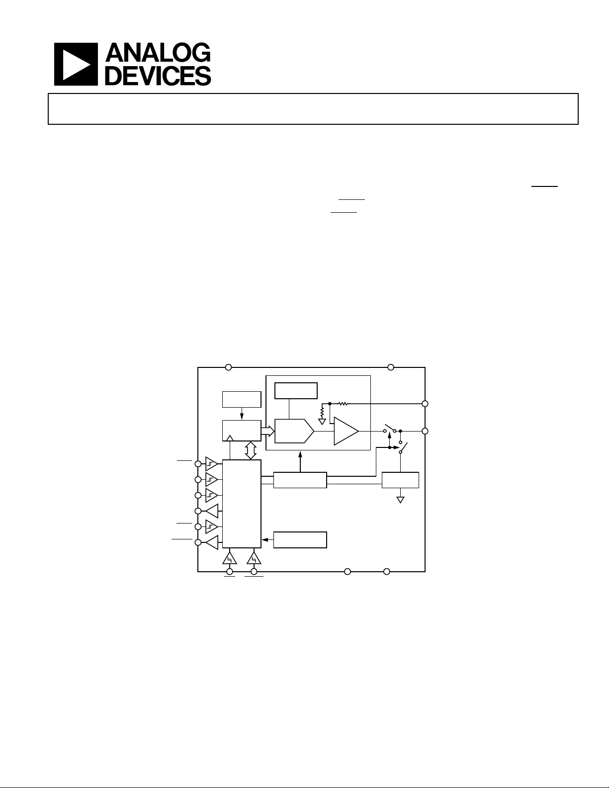
GENERAL DESCRIPTION
The AD5501 is a single-channel, 12-bit, serial input, digital-toanalog converter (DAC) with an on-chip high voltage output
amplifier and an integrated precision reference. The DAC output
voltage range is programmable via the range select pin (
R_SEL
If
R_SEL
is held high, the DAC output range is 0 V to 30 V. If
is held low, the DAC output range is 0 V to 60 V. The on
chip output amplifier allows an output swing within the range
of AGND + 0.5 V to V
− 0.5 V.
DD
The AD5501 has a high speed serial interface, which is compatible
with SPI®-, QSPI™-, MICROWIRE™-, and DSP-interface standards
and can handle clock speeds of up to 16.667 MHz.
R_SEL
).
FUNCTIONAL BLOCK DIAGRAM
Figure 1.
responsibility is assumed by Analog Devices for its use, nor for any infringements of patents or other
rights of third parties that may result from its use. Specifications subject to change without notice. No
license is granted by implication or otherwise under any patent or patent rights of Analog Devices.
One Technology Way, P.O. Box 9106, Norwood, MA 02062-9106, U.S.A.
Tel: 781.329.4700 ©2009-2012 Analog Devices, Inc. All rights reserved.
Page 2

AD5501 Data Sheet
TABLE OF CONTENTS
Features .............................................................................................. 1
Applications ....................................................................................... 1
General Description ......................................................................... 1
Functional Block Diagram .............................................................. 1
Revision History ............................................................................... 2
Specifications ..................................................................................... 4
AC Characteristics ........................................................................ 5
Timing Characteristics ................................................................ 6
Absolute Maximum Ratings ............................................................ 8
Thermal Resistance ...................................................................... 8
ESD Caution .................................................................................. 8
Pin Configuration and Function Descriptions ............................. 9
Typical Performance Characteristics ........................................... 10
Terminology .................................................................................... 12
Theory of Operation ...................................................................... 13
Power-Up State ........................................................................... 13
Power-Down Mode .................................................................... 13
DAC Channel Architecture ....................................................... 13
VFB Pin .......................................................................................... 13
Selecting the Output Range ...................................................... 14
CLR
Function.............................................................................. 14
LDAC
Function .......................................................................... 14
Temperature Sensor ................................................................... 14
Power Dissipation....................................................................... 14
Power Supply Sequencing ......................................................... 14
Serial Interface ................................................................................ 15
Writ e Mode ................................................................................. 15
Read Mode .................................................................................. 15
Writing to the Control Register ................................................ 15
Interfacing Examples ................................................................. 16
Outline Dimensions ....................................................................... 17
Ordering Guide .......................................................................... 17
REVISION HISTORY
12/12—Rev. B to Rev. C
Changes to t
Changes to Figure 3 and Figure 4 ................................................... 7
Changes to Pin 2 Description, Table 7 and Pin 3 Description,
Tabl e 7 ................................................................................................ 9
Changes to Write Mode Section ................................................... 15
Changes to Table 10 ........................................................................ 16
Parameter, Table 4 .................................................... 6
4
4/12—Rev. A to Rev. B
Changes to Product Title .................................................................. 1
Changes to Figure 15 and Figure 16 ............................................ 13
10/10—Rev. 0 to Rev. A
Changes to Figure 3 and Figure 4 .................................................... 7
7/09—Revision 0: Initial Version
Rev. C | Page 2 of 20
Page 3

Data Sheet AD5501
The serial interface offers the user the capability of both writing
to, and reading from, most internal registers.
To reduce power consumption at power up, only the digital
section of the AD5501 is powered up initially. This gives the
user the ability to program the DAC registers to the required
value while typically consuming only 30 μA of supply current.
The AD5501 incorporates power-on reset circuitry that ensures
the DAC registers power up in a known condition and remain
there until a valid write to the device has occurred. The analog
section is powered up by issuing a power-up command via the
SPI interface. The AD5501 provides software-selectable output
loads while in the power-down mode.
The AD5501 has on on-chip temperature sensor. If the temperature on the die exceeds 110°C, the
low CMOS output pin) flags an alarm and the AD5501 enters
a temperature power-down mode that disconnects the output
amplifier, thus removing the short-circuit condition. The AD5501
remains in power-down mode until a software power-up
command is executed.
The AD5501 is available in a compact 16-lead TSSOP. The AD5501
is guaranteed to operate over the extended temperature range of
−40°C to +105°C.
Table 1. Related Device
Part No. Description
AD5504 High Voltage, Quad Channel 12-Bit Voltage Output DAC
ALARM
pin (an active
Rev. C | Page 3 of 20
Page 4

AD5501 Data Sheet
V
OUT
Temperature Coefficient
3, 4
50 ppm/°C
DAC code = half scale
ZSE
FSE
Feedback Resistance7
100 Ω
DIGITAL INPUTS
LOGIC
LOGIC
LOGIC
LOGIC
SOURCE
SINK
SPECIFICATIONS
VDD = 10 V to 62 V; V
Table 2.
Parameter Symbol Min Typ1 Max Unit Test Conditions/Comments
ACCURACY2
Resolution 12 Bits
Differential Nonlinearity DNL −1 +1 LSB
Integral Nonlinearity INL
60 V Mode −1 +1 LSB VDD = 62 V
30 V Mode −2 +2 LSB VDD = 62 V
Offset Error VOE −65 +100 mV
Offset Error Drift4 60 µV/°C
Zero-Scale Error V
Zero-Scale Error Drift4 50 µV/°C 60 V mode
Full-Scale Error V
Full-Scale Error Drift4 1 mV/°C −40°C to +25°C; 60 V mode
350 µV/°C +25°C to +105°C; 60 V mode
Gain Error −0.6 +0.6 % of FSR
Gain Temperature Coefficient4 10 ppm of FSR/°C
OUTPUT CHARACTERISTICS
Output Voltage Range5 AGND + 0.5 VDD − 0.5 V
Short-Circuit Current
Capacitive Load Stability4 1 V to 4 V step
RL = 60 kΩ to ∞ 1 nF
Load Current4 −1 +1 mA
= 2.3 V to 5.5 V; RL = 60 kΩ; CL = 200 pF; −40°C < TA < +105°C, unless otherwise noted.
LOG IC
80 mV
−325 +275 mV
4, 6
2 mA
DC Output Impedance4 3 Ω
DC Output Leakage4 10 µA
Input Logic High VIH 2.0 V V
1.8 V V
Input Logic Low VIL 0.8 V V
Input Current IIL ±1 µA
Input Capacitance4 IIC 5 pF
DIGITAL OUTPUTS
Output High Voltage VOH V
− 0.4 V V I
Output Low Voltage VOL DGND + 0.4 V V I
Three-State Leakage Current
SDI, SDO, SCLK,
R_SEL
Pin −10 +10 µA
ALARM
LDAC, CLR
Pins
,
−1 +1 µA
Output Capacitance4 5 pF
= 4.5 V to 5.5 V
= 2.3 V to 3.6 V
= 2.3 V to 5.5 V
= 200 µA
= 200 µA
Rev. C | Page 4 of 20
Page 5
Data Sheet AD5501
LOGIC
LOGI C
LOGIC
DD_PWD
TOTAL
Parameter Symbol Min Typ1 Max Unit Test Conditions/Comments
POWER SUPPLIES
VDD 10 62 V
V
2.3 5.5 V
Quiescent Supply Current I
Logic Supply Current I
DC PSRR4
30 V mode 76 dB DAC output = full scale
60 V mode 68 dB DAC output = full scale
POWER-DOWN MODE
Supply Current I
Software Power-Down Mode 30 50 µA
Junction Temperature6 TJ 130 °C TJ = TA + P
1
Typical specifications represent average readings at 25°C, VDD = 62 V, and V
2
Valid in the output voltage range of (AGND + 0.5 V) to (VDD − 0.5 V). Output is unloaded.
3
Includes linearity, offset, and gain drift.
4
Guaranteed by design and characterization. Not production tested.
5
The DAC architecture gives a fixed linear voltage output range of 0 V to 30 V if
limited by output amplifier compliance, V
6
If the die temperature exceeds 110°C, the AD5501 enters a temperature power-down mode putting the DAC output into a high impedance state thereby removing
the short-circuit condition. Overheating caused by long term short-circuit condition(s) is detected by an integrated thermal sensor. After power-down, the AD5501
remains powered down until a software power-up command is executed.
7
Maximum resistance between V
OUT
should be set to at least 0.5 V higher than the maximum output voltage to ensure compliance.
DD
and VFB pins.
0.6 0.75 mA Static conditions; DAC output =
QUIESCENT
midscale
0.4 2 µA VIH = V
; VIL = DGND
× θJA
= 5 V.
LOGIC
R_SEL
is held high and 0 V to 60 V if
R_SEL
is held low. As the output voltage range is
AC CHARACTERISTICS
VDD = 10 V to 62 V; V
able 3.
T
Parameter
1, 2
AC CHARACTERISTICS
Output Voltage Settling Time ¼ to ¾ scale settling to ±1 LSB, RL = 60 kΩ
60 V Mode 45 55 µs
30 V Mode 25 35 µs
Slew Rate 0.65 V/µs
Digital-to-Analog Glitch Energy 300 nV-s 1 LSB change around major carry in 60 V mode
Glitch Impulse Peak Amplitude 170 mV 60 V mode
Digital Feedthrough 5 nV-s
Peak-to-Peak Noise 140 μV p-p 0.1 Hz to 10 Hz; DAC code = 0x800
4 mV p-p 0.1 Hz to 10 kHz; DAC code = 0x800
1
Guaranteed by design and characterization; not production tested.
2
See the Terminology section.
3
Temperature range is −40°C to + 105°C, typical at 25°C.
= 2.3 V to 5.5 V; RL = 60 kΩ; CL = 200 pF; −40°C < TA < +105°C, unless otherwise noted.
LOG IC
Min Typ Max Unit Test Conditions/Comments3
Rev. C | Page 5 of 20
Page 6
AD5501 Data Sheet
1
2
t6 5 ns min
Data hold time
15
16
t
17
4
50
μs max
Power-on-reset time (this is not shown in the timing figures)
18
5
V
OH
(MIN) – VOL (MAX)
2
200µA I
OL
200µA I
OH
TO OUTPUT
PIN
C
L
50pF
07992-002
TIMING CHARACTERISTICS
VDD = 30 V, V
Table 4.
Parameter Limit1 Unit Test Conditions/Comments
t
60 ns min SCLK cycle time
t2 10 ns min SCLK high time
t3 10 ns min SCLK low time
t4 25 ns min
t5 15 ns min Data setup time
= 2.3 V to 5.5 V, and −40°C < TA < +105°C, all specifications T
LOG IC
falling edge to SCLK rising edge setup time
SYNC
MIN
to T
, unless otherwise noted.
MAX
t7 0 ns min SCLK falling edge to
t8 20 ns min Minimum
t9 20 ns min
pulse width low
LDAC
SYNC
high time
t10 50 ns min SCLK falling edge to
t11 15 ns min
t12 100 ns typ
t13 20 μs typ
pulse width low
CLR
pulse activation time
CLR
clear time
ALARM
SYNC
LDAC
rising edge
rising edge
t14 110 ns min SCLK cycle time in read mode
3
t
55 ns max SCLK rising edge to SDO valid
3
t
25 ns min SCLK to SDO Data hold time
t
50 μs max Power-on time (this is not shown in the timing figures)
t19 5 μs typ
1
All input signals are specified with tr = tf = 1 ns/V (10% to 90% of VDD) and timed from a voltage level of (VIL + VIH)/2.
2
Maximum SCLK frequency is 16.667 MHz.
3
Under the load conditions that are outlined in Figure 2.
4
Time from when VDD or V
5
Time required from execution of power-on software command to when the DAC output has settled to 1 V.
supplies are powered-up to when a digital interface command can be executed.
LOGIC
clear to output amplifier turn on (this is not shown in the timing figures)
ALARM
Circuit and Timing Diagrams
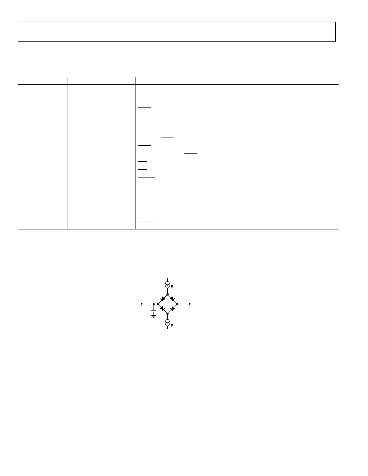
Figure 2. Load Circuit for SDO Timing Diagram
Rev. C | Page 6 of 20
Page 7

Data Sheet AD5501
07994-003
1
ASYNCHRONOUS LDAC UPDATE MODE.
2
SYNCHRONOUS LDAC UPDATE MODE.
3
IN THE EVENT OF OVERTEMPERATURE CONDITION.
SCLK
SDI
CLR
SYNC
LDAC
1
LDAC
2
ALARM
3
V
OUT
R/W
D0
t
4
t
8
t
3
t
1
t
2
t
7
t
5
t
6
t
9
t
10
t
11
t
12
t
13
SCLK
SYNC
SDI
SDO
t
14
D11
D0
R/W
A2 A1 A0 X X X
D10 D9 D8 D1D2
X X X X
t
15
t
16
07994-004
Figure 3. Write Timing Diagram
Figure 4. Read Timing Diagram
Rev. C | Page 7 of 20
Page 8

AD5501 Data Sheet
VDD to AGND
−0.3 V to +64 V
LOGIC
OUT
LOGIC
LOGIC
AGND to DGND
−0.3 V to +0.3 V
J
Time at Peak Temperature Range
20 sec to 40 sec
ABSOLUTE MAXIMUM RATINGS
TA = 25°C, unless otherwise noted. Transient currents of up to
100 mA do not cause SCR latch-up.
Table 5.
Parameter Rating
V
to DGND −0.3 V to +7 V
V
to AGND −0.3 V to VDD + 0.3 V
Digital Input to DGND −0.3 V to V
SDO Output to DGND −0.3 V to V
Maximum Junction Temperature
(T
Maximum)
Storage Temperature Range −65°C to +150°C
Reflow Soldering
Peak Temperature 260°C
150°C
+ 0.3 V
+ 0.3 V
Stresses above those listed under Absolute Maximum Ratings
may cause permanent damage to the device. This is a stress
rating only; functional operation of the device at these or any
other conditions above those indicated in the operational
section of this specification is not implied. Exposure to absolute
maximum rating conditions for extended periods may affect
device reliability.
THERMAL RESISTANCE
θJA is specified for the worst-case conditions, that is, a device
soldered in a circuit board for surface-mount packages.
Thermal resistance is for a JEDEC 4-layer (2S2P) printed circuit
board (PCB).
Table 6. Thermal Resistance
Package Type θJA Unit
16-Lead TSSOP 112.60 °C/W
ESD CAUTION
Rev. C | Page 8 of 20
Page 9

Data Sheet AD5501
NC = NO CONNECT
1
2
3
4
5
6
7
8
SYNC
SCLK
SDI
AGND
DGND
SDO
CLR
LDAC
16
15
14
13
12
11
10
9
ALARM
V
DD
R_SEL
NC
NC
V
FB
V
OUT
V
LOGIC
TOP VIEW
(Not to S cale)
AD5501
07992-005
OUT
LOGIC
PIN CONFIGURATION AND FUNCTION DESCRIPTIONS
Figure 5. Pin Configuration
Table 7. Pin Function Descriptions
Pin No. Mnemonic Description
1
2
Asynchronous Clear Input. The
CLR
When
Falling Edge Synchronization Signal. This is the frame synchronization signal for the input data. When
SYNC
is activated, the input register and the DAC register are set to 0x000 and the output to zero scale.
CLR
input is falling edge sensitive. When
CLR
is low, all
CLR
pulses are ignored.
LDAC
SYNC
goes low, it
enables the input shift register and data is transferred in on the rising edges of the following clocks. The selected
DAC register is updated on the 16th falling SCLK, unless
edge of
acts as an interrupt, and the write sequence is ignored by the DAC.
SYNC
is taken high before this edge, in which case, the rising
SYNC
3 SCLK Serial Data Input. This part has a 16-bit shift register. Data is clocked into the register on the rising edge of the serial
clock input.
4 SDI Serial Data Input. This part has a 16-bit shift register. Data is clocked into the register on the falling edge of the serial clock
input.
5 SDO Serial Data Output. CMOS output. This pin serves as the readback function for all DAC and control registers. Data is
clocked out on the rising edge of SCLK and is valid on the falling edge of SCLK.
6 DGND Digital Ground Pin.
7 AGND Analog Ground Pin.
8
Load DAC Input. Pulsing this pin low updates the DAC with the value in the input register. If the
LDAC
pin is tied low, the
LDAC
DAC output is updated automatically when data is written to the input register.
9, 10 NC Not Connected. These pins remain unconnected.
11 VFB Voltage Feedback Pin. Feedback node for the output amplifier.
12 V
13
Buffered Analog Output Voltage from the DAC.
Range Select Pin. Tying this pin to DGND selects a DAC output range of 0 V to 60 V, alternatively tying
R_SEL
R_SEL
to V
LOGI C
selects a DAC output range of 0 V to 30 V.
14 VDD Positive Analog Power Supply. 10 V to 62 V for the specified performance. Decouple this pin with 0.1µF ceramic
capacitors and 10 µF capacitors.
15
16 V
Active Low CMOS Output Pin. Flags an alarm if the temperature on the die exceeds 110°C.
ALARM
Logic Power Supply; 2.3 V to 5.5 V. Decouple this with 0.1 µF ceramic capacitors and 10 µF capacitors.
Rev. C | Page 9 of 20
Page 10

AD5501 Data Sheet
0.8
–0.8
–0.4
0
0.4
32 1008 2048 3056 4064
INL (LSB)
CODE
07992-006
0.50
–0.50
–0.25
0
0.25
32 1008 2048 3056 4064
DNL (LSB)
CODE
07992-007
15.0050
14.9950
14.9975
15.0000
15.0025
0 0.05 0.10 0.15 0.20
V
OUT
(V)
TIME (ms)
07992-008
0 0.05 0.10 0.15 0.20
V
OUT
(V)
TIME (ms)
45.0025
45.0000
44.9975
44.9950
44.9925
07992-009
0 2.5 5.0 7.5 10.0
OUTPUT VOLTAGE (µV)
TIME (Seconds)
200
100
0
–100
–200
V
DD
= 62V
V
OUT
= 30V
07992-010
0 15 30 45 60
I
DD
(mA)
V
OUT
(V)
0.70
0.65
0.60
0.55
0.50
VDD = 62V
07992-011
TYPICAL PERFORMANCE CHARACTERISTICS
Figure 6. Typical INL
Figure 7. Typical DNL
Figure 9. Output Settling Time (Low to High)
Figure 10. Output Noise
Figure 8. Output Settling Time (High to Low)
Figure 11. IDD vs. V
OUT
Rev. C | Page 10 of 20
Page 11

Data Sheet AD5501
0 5 10 15
AMPLITUDE (LSB)
TIME (ms)
2
–10
–8
–6
–4
–2
0
07992-012
0 5 10 15
AMPLITUDE (LSB)
TIME (ms)
12
–4
–2
0
2
4
6
8
10
07992-013
Figure 12. Digital-to-Analog Negative Glitch Impulse
Figure 13. Digital-to-Analog Positive Glitch Impulse
Rev. C | Page 11 of 20
Page 12

AD5501 Data Sheet
TERMINOLOGY
Relative Accuracy (Integral Nonlinearity)
For the DAC, relative accuracy, or integral nonlinearity (INL), is
a measure of the maximum deviation in LSBs from a straight line
passing through the endpoints of the DAC transfer function.
Differential Nonlinearity
Differential nonlinearity (DNL) is the difference between the
measured change and the ideal 1 LSB change between any two
adjacent codes. A specified differential nonlinearity of ±1 LSB
maximum ensures monotonicity. This DAC is guaranteed
monotonic by design.
Zero-Code Error
Zero-code error is a measure of the output error when zero code
(0x000) is loaded into the DAC register. Ideally, the output
should be 0 V. The zero-code error is always positive in the
AD5501 because the output of the DAC cannot go below 0 V
due to a combination of the offset errors in the DAC and the
output amplifier. Zero-code error is expressed in millivolts.
Zero-Code Error Drift
Zero-code error drift is a measure of the change in zero-code error
with a change in temperature expressed in μV/°C.
Offset Error
A measure of the difference between V
(actual) and V
OUT
OUT
(ideal)
expressed in millivolts in the linear region of the transfer function.
Offset error is measured on the AD5501 with Code 32 loaded in
the DAC registers for 60 V mode and with Code 64 loaded in
the DAC registers for 30 V mode. Offset error is expressed in
millivolts.
Offset Error Drift
Offset error drift is a measure of the change in offset error with
a change in temperature. It is expressed in μV/°C.
Full-Scale Error
Full-scale error is a measure of the output error when full-scale
code (0xFFF) is loaded into the DAC register expressed in
millivolts.
Full-Scale Error Drift
Full-scale error drift is a measure of the change in full-scale
error with a change in temperature. It is expressed in μV/°C.
Gain Error
Gain error is a measure of the span error of the DAC. It is the
deviation in slope of the DAC transfer characteristic from the
ideal, expressed as a percentage of the full-scale range.
Gain Temperature Coefficient
The gain temperature coefficient is a measure of the change in
gain with changes in temperature. It is expressed in (ppm of
full-scale range)/°C.
Digital-to-Analog Glitch Impulse
Digital-to-analog glitch impulse is the impulse injected into the
analog output when the input code in the DAC register changes
state. It is normally specified as the area of the glitch in nV-s
and is measured when the digital input code is changed by
1 LSB at the major carry transition.
DC Power Supply Rejection Ratio (PSRR)
PSRR indicates how the output of the DAC is affected by changes
in the supply voltage. PSRR is the ratio of the change in V
a change in V
in decibels. V
for full-scale output of the DAC. It is measured
DD
is dc varied ±10%.
DD
OUT
to
AC Power Supply Rejection Ratio (PSRR)
PSRR indicates how the output of the DAC is affected by changes
in the supply voltage. PSRR is the ratio of the change in V
a change in V
in decibels. V
for full-scale output of the DAC. It is measured
DD
is ac varied ±10%.
DD
OUT
to
Digital Feedthrough
Digital feedthrough is a measure of the impulse injected into
the analog output of the DAC from the digital input pins of the
device but is measured when the DAC is not being written to
SYNC
(
held high). It is specified in nV-s and measured with a
full-scale change on the digital input pins, that is, from all 0s to
all 1s or vice versa.
Capacitive Load Stability
Capacitive load stability refers to the ability of the amplifier to
drive a capacitive load. An amplifier output is considered stable
if any overshoot or ringing has stopped before approximately
1.5 times the settling time of the DAC has elapsed.
Rev. C | Page 12 of 20
Page 13

Range
D
V
OUT
×=
4096
GAIN
V
OUT
DAC
REGISTER
INPUT
REGISTER
PRECISION
REFERENCE
AGND
1212
DAC
07992-014
V
FB
R
L
OUTPUT
BUFFER
12-BIT
DAC
1713kΩ
122.36kΩ
V
OUT
07992-015
V
FB
OUTPUT
BUFFER
12-BIT
DAC
1713kΩ
122.36kΩ
V
OUT
R
L
V
DD
07992-016
R
Data Sheet AD5501
THEORY OF OPERATION
The AD5501 contains a 12-bit DAC, an output amplifier, and a
precision reference in a single package. The architecture of the
DAC channel consists of a 12-bit resistor string DAC followed
by an output buffer amplifier. The part operates from a singlesupply voltage of 10 V to 62 V. The DAC output voltage range is
selected via the range select,
is 0 V to 30 V if
R_SEL
R_SEL
, pin. The DAC output range
is held high and 0 V to 60 V if
held low. Data is written to the AD5501 in a 16-bit word format
(see Tabl e 8), via a serial interface.
POWER-UP STATE
On power-up, the power-on reset circuitry clears the bits of the
control register to 0x40 (see Table 10) ensuring that the analog
section is initially powered down, which helps reduce power
consumption. The user can program the DAC register to the
required value while typically consuming only 30
µA of supply
current. The power-on reset circuitry also ensures that the input
and DAC registers power up in a known condition, 0x000, and
remain there until a valid write to the device has taken place.
The analog section can be powered up by setting Bit C2 of the
control register to 1.
POWER-DOWN MODE
The DAC channel can be powered up or powered down by
programming Bit C2 in the control register (see Tab l e 10). When
the DAC channel is powered down, the associated analog circuitry
turns off to reduce power consumption. The digital section of
the AD5501 remains powered up. The output of the DAC amplifier
can be three-stated or connected to AGND via an internal 20 kΩ
resistor, depending on the state of Bit C6 in the control register.
The power-down mode does not change the contents of the DAC
register to ensure that the DAC channel returns to its previous
voltage when the power-down bit is set to 1. The AD5501 also
offers the user the flexibility of updating the DAC registers during
power-down. The control register can be read back at any time
to check the status of the bits.
DAC CHANNEL ARCHITECTURE
The architecture of the DAC channel consists of a 12-bit resistor
string DAC followed by an output buffer amplifier (see Figure 14).
The resistor string section is simply a string of resistors, each of
Value R from V
This type of architecture guarantees DAC monotonicity. The 12-bit
binary digital code loaded to the DAC register determines at which
node on the string the voltage is tapped off before being fed into
the output amplifier. The output amplifier multiplies the DAC
output voltage to give a fixed linear voltage output range of 0 V
to 60 V if
R_SEL
amplifier is capable of driving a 60 kΩ load while allowing an
output swing within the range of AGND + 0.5 V to V
generated by the precision reference to AGND.
REF
= 0 or 0 V to 30 V if
R_SEL
= 1. Each output
R_SEL
is
− 0.5 V.
DD
Rev. C | Page 13 of 20
Because the DAC architecture gives a fixed voltage output range
of 0 V to 30 V or 0 V to 60 V, the user should set V
DD
30.5 V or 60.5 V to use the maximum DAC resolution. The data
format for the AD5501 is straight binary and the output voltage
follows the formula
where:
D is the code loaded to the DAC.
Range = 30, if
R_SEL
is high, and 60 if
Figure 14. DAC Channel Architecture
R_SEL
is low.
VFB PIN
The voltage feedback pin (VFB) is part of the feedback loop of
the gain amplifier. To compensate for any voltage drop between the
V
pin and the load, connect (in a force sense configuration) VFB
OUT
to the V
The VFB pin can also be used to control a pass transistor where
more current is required than can be supplied by the AD5501.
The configuration is shown in Figure 16.
pin, as shown in Figure 15.
OUT
Figure 15. V
Figure 16. Pass Transistor Configuration
and V
FB
Configuration
OUT
to at least
Page 14

AD5501 Data Sheet
SELECTING THE OUTPUT RANGE
The output range of the DAC is selected by the
R_SEL
the
pin is connected to a Logic 1, the DAC output voltage
can be set between 0 V and 30 V. When the
to a Logic 0, the DAC output voltage can be set between 0 V and
R_SEL
60 V. The state of
can be changed any time when the serial
interface is not being used, that is, not during a read or write
operation. When the
R_SEL
pin is changed, the voltage on the
output pin remains the same until the next write to the DAC
LDAC
register (and
is brought low). For example, if the user
writes 0x800 to the DAC register when in 30 V mode (
the output voltage is 15 V (assuming
pulsed low). When the user switches to 60 V mode (
the output stays at 15 V until the user writes a new value to the
LDAC
DAC register.
must be low or be pulsed low for the output to
change.
FUNCTION
CLR
The AD5501 has a hardware
clear input. The
CLR
line low clears the contents of the input register and the DAC
CLR
input is falling edge sensitive. Bringing the
registers to 0x000. The
CLR
edge of
LDAC
to when the output starts to change, is typically 100 ns.
FUNCTION
CLR
pin that is an asynchronous
CLR
pulse activation time, that is, the falling
The DAC output can be updated using the hardware
LDAC
is normally high. On the falling edge of
copied from the input register to the DAC register and the DAC
output is updated (asynchronous update mode, see Figure 3). If
LDAC
the
is kept low or is low on the falling edge of the 16th SCLK,
the DAC register and DAC output are updated automatically
when new data is received in the input register (synchronous
update mode, see Figure 3).
R_SEL
R_SEL
LDAC
is low or has been
LDAC
pin. When
pin is connected
R_SEL
= 1),
R_SEL
= 0),
LDAC
pin.
, data is
TEMPERATURE SENSOR
The AD5501 has an integrated temperature sensor, which causes
the part to enter thermal shutdown mode when the temperature
on the die exceeds 110°C. In thermal shutdown mode, the analog
section of the device powers down and the DAC output is
disconnected but the digital section remains operational, which
is equivalent to setting the power-down bit in the control register.
To indicate that the AD5501 has entered temperature shutdown
mode, Bit 0 of the control register is set to 1 and the
ALARM
pin goes low. The AD5501 remains in temperature shutdown
mode with Bit 0 set to 1 and the
ALARM
pin low, even if the die
temperature falls, until Bit 0 in the control register is cleared to 0.
POWER DISSIPATION
Drawing current from the V
the die and package of the AD5501. The package junction
temperature (T
) should not exceed 130°C for normal operation. If
J
the die temperature exceeds 110°C, the AD5501 enters thermal
shutdown mode as described in the previous section. The amount
of heat generated can be calculated using the formula
T
= TA + (P
J
TOTAL
× θJA)
where:
T
is the package junction temperature.
J
T
is the ambient temperature.
A
P
is the total power being consumed by the AD5501.
TO TAL
θ
is the thermal impedance of the AD5501 package (see the
JA
Absolute Maximum Ratings section for this value).
pin causes a temperature rise in
OUT
POWER SUPPLY SEQUENCING
The power supplies for the AD5501 can be applied in any order
without affecting the device. However, before the power supplies
are applied, connect the AGND and DGND pins to the relevant
ground plane. Do not allow any of the digital input pins (SCLK,
SYNC, R_SEL
SDI,
digital input pins can be connected to pull-up (to V
pull-down (to DGND) resistors as required.
, and
CLR
) to float during power up. The
LOGIC
) or
Rev. C | Page 14 of 20
Page 15

Data Sheet AD5501
1 1 1 Control register
SERIAL INTERFACE
The AD5501 has a serial interface (
SYNC
, SCLK, SDI, and
SDO), which is compatible with SPI standards, as well as with
most DSPs. The AD5501 allows writing of data, via the serial
interface, to the input and control registers. The DAC register is
not directly writeable or readable.
The input shift register is 16 bits wide (see Table 8). The 16-bit
word consists of one read/write (R/
W
) control bit, followed by
three address bits and 12 DAC data bits. Data is loaded MSB first.
WRITE MODE
To write to a register, the R/W bit should be 0. The three address
bits in the input register (see Ta ble 9) then determine the register to
update. The address bits (A2 to A0) should be 001 to write to the
DAC input register or 111 to write to the control register. Data
is clocked into the selected register during the remaining 12 clocks
of the same frame. Figure 3 shows a timing diagram of a typical
AD5501 write sequence. The write sequence begins by bringing
SYNC
the
shift register on the rising edge of SCLK. On the 16th falling
clock edge, the last data bit is clocked in and the programmed
function is executed (that is, a change in the selected DAC input
register or a change in the mode of operation). The AD5501 does
not require a continuous SCLK and dynamic power can be saved
by transmitting clock pulses during a serial write only. At this
stage, the
case, it must be brought high for a minimum of 20 ns before the
next write sequence for a falling edge of
write sequence. Operate all interface pins close to the supply
rails to minimize power consumption in the digital input buffers.
line low. Data on the SDI line is clocked into the 16-bit
SYNC
line can be kept low or be brought high. In either
SYNC
to initiate the next
READ MODE
The AD5501 allows data readback via the serial interface from
the DAC input register and the control register. To read back a
register, it is first necessary to tell the AD5501 that a readback is
required. This is achieved by setting the R/
W
bit to 1. The three
address bits then determine the register from which data is to
be read back. Data from the selected register is clocked out of
the SDO pin on the next 12 clocks of the same frame.
The SDO pin is normally three-stated but becomes driven on the
rising edge of the fifth clock pulse. The pin remains driven until the
data from the register has been clocked out or the
SYNC
pin is
returned high. Figure 4 shows the timing requirements during a
read operation. Note that due to timing requirements of t
14
(110 ns), the maximum speed of the SPI interface during a read
operation should not exceed 9 MHz.
WRITING TO THE CONTROL REGISTER
The control register is written when Bits[DB14:DB12] are 1. The
control register sets the power-up state of the DAC output. A
write to the control register must be followed by another write
operation. The second write operation can be a write to a DAC
input register or a NOP write. Figure 17 shows some typical
combinations.
Table 8. Input Register Bit Map
DB15 DB14 DB13 DB12 DB11 DB10 DB9 DB8 DB7 DB6 DB5 DB4 DB3 DB2 DB1 DB0
R/W
A2 A1 A0 Data
Table 9. Input Register Bit Functions
Bit Description
R/W
A2, A1, A0 These bits determine if the input register or the control register is to be accessed.
0 0 0 NOP1
0 0 1 DAC input register
0 1 0 Reserved
0 1 1 Reserved
1 0 0 Reserved
1 0 1 Reserved
1 1 0 Reserved
D11:D0 Data bits.
1
No operation command
Indicates a read from or a write to the addressed register.
A2 A1 A0 Function
Rev. C | Page 15 of 20
Page 16

AD5501 Data Sheet
07994-120
WRITE N WRITE N + 1
WRITE TO
CONTROL REGISTER
NOP
WRITE TO
CONTROL REGISTER
WRITE TO
DAC REGIST E R
WRITE N + 2
WRITE TO
CONTROL REGISTER
WRITE TO
CONTROL REGISTER
NOP
WRITE TO
CONTROL REGISTER
WRITE TO
CONTROL REGISTER
WRITE TO
DAC REGIST E R
SPISELx
ADSP-BF531
AD5501
SCK
MOSI
MISO
PF10
PF8
PF9
PF7
SYNC
SCLK
SDI
SDO
R_SEL
CLR
LDAC
ALARM
07992-017
SYNC
SCLK
SDI
SDO
R_SEL
CLR
LDAC
ALARM
AD5501
ADSP-21065L
TFSx
RFSx
TCLKx
RCLKx
DTxA
DRxA
FLAG
0
FLAG
1
FLAG
2
FLAG
3
07992-018
Table 10. Control Register Functions Bit Map
DB15 DB14 DB13 DB12 DB11 DB10 DB9 DB8 DB7 DB6 DB5 DB4 DB3 DB2 DB1 DB01
R/W
1
Read only bit. This bit should be 0 when writing to the control register
Table 11. Control Register Function Bit Descriptions
Bit No. Bit Name Description
DB0 C0 C0 = 0: the device is not in thermal shutdown mode.
C0 = 1: the thermal shutdown mode is activated.
DB1 C1 C1 = 0: reserved. This bit should be 0 when writing to the control register.
DB2 C2 C2 = 0: DAC channel power-down (default).
C2 = 1: DAC channel power-up.
DB[3:5] C3 to C5 C3 to C5 = 0: reserved. These bits should be 0 when writing to the control register.
DB6 C6 C6 = 0: output connected to AGND through a 20 kΩ resistor.
C6 = 1: output is three-stated (default).
1 1 1 0 0 0 0 0 C6 C5 C4 C3 C2 C1 C0
INTERFACING EXAMPLES
The SPI interface of the AD5501 is designed to allow it to be easily
connected to industry-standard DSPs and microcontrollers.
Figure 18 shows how the AD5501 can be connected to the Analog
Devices, Inc., Blackfin® DSP. The Blackfin has an integrated SPI
port that can be connected directly to the SPI pins of the AD5501.
Programmable input/output pins are also available and can be
used to read or set the state of the digital input or output pins
associated with the interface.
Figure 18. Interfacing to a Blackfin DSP
Figure 17. Control Register Write Sequences
The Analog Devices ADSP-21065L is a floating point DSP with
two serial ports (SPORTs). Figure 19 shows how one SPORT
can be used to control the AD5501. In this example, the transmit
frame synchronization (TFS) pin is connected to the receive frame
synchronization (RFS) pin. The transmit and receive clocks (TCLK
and RCLK) are also connected together. The user can write to the
AD5501 by writing to the transmit register. When a read operation
is performed, the data is clocked out of the AD5501 on the last
12 SCLKs. The DSP receive interrupt can be used to indicate when
the read operation is complete.
Rev. C | Page 16 of 20
Figure 19. Interfacing to an ADSP-21065L DSP
Page 17

Data Sheet AD5501
16
9
81
PIN 1
SEATING
PLANE
8°
0°
4.50
4.40
4.30
6.40
BSC
5.10
5.00
4.90
0.65
BSC
0.15
0.05
1.20
MAX
0.20
0.09
0.75
0.60
0.45
0.30
0.19
COPLANARITY
0.10
COMPLIANT TO JEDEC STANDARDS MO-153-AB
EVAL-AD5501EBZ
Evaluation Board
OUTLINE DIMENSIONS
Figure 20. 16-Lead Thin Shrink Small Outline Package [TSSOP]
(RU-16)
Dimensions shown in millimeters
ORDERING GUIDE
Model1 Temperature Range Package Description Package Option
AD5501BRUZ −40°C to +105°C 16-Lead Thin Shrink Small Outline Package [TSSOP] RU-16
AD5501BRUZ-REEL −40°C to +105°C 16-Lead Thin Shrink Small Outline Package [TSSOP] RU-16
1
Z = RoHS Compliant Part.
Rev. C | Page 17 of 20
Page 18

AD5501 Data Sheet
NOTES
Rev. C | Page 18 of 20
Page 19

Data Sheet AD5501
NOTES
Rev. C | Page 19 of 20
Page 20

AD5501 Data Sheet
©2009-2012 Analog Devices, Inc. All rights reserved. Trademarks and
NOTES
registered trademarks are the property of their respective owners.
D07992-0-12/12(C)
Rev. C | Page 20 of 20
 Loading...