

Page 1
1 pA Monolithic Electrometer
a
FEATURES
DC PERFORMANCE
1 mV max Input Offset Voltage
Low Offset Drift: 20 mV/8C
1 pA max Input Bias Current
Input Bias Current Guaranteed Over Full
Common-Mode Voltage Range
AC PERFORMANCE
3 V/ms Slew Rate
1 MHz Unity Gain Bandwidth
Low Input Voltage Noise: 4 mV p-p, 0.1 Hz to 10 Hz
Available in a Low Cost, 8-Pin Plastic Mini-DIP
Standard Op Amp Pinout
APPLICATIONS
Electrometer Amplifiers
Photodiode Preamps
pH Electrode Buffers
Log Ratio Amplifiers
Operational Amplifier
AD546*
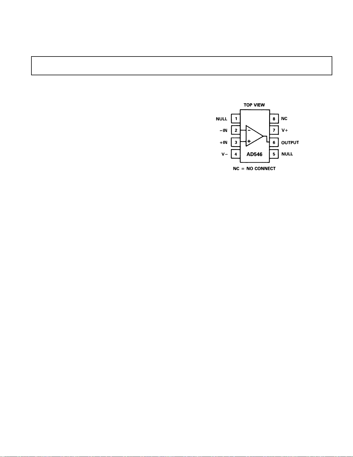
CONNECTION DIAGRAM
8-Pin Plastic
Mini-DIP Package
PRODUCT DESCRIPTION
The AD546 is a monolithic electrometer combining the virtues
of low (1 pA) input bias current with the cost effectiveness of a
plastic mini-DIP package. Both input offset voltage and input
offset voltage drift are laser trimmed, providing very high performance for such a low cost amplifier.
Input bias currents are reduced significantly by using “topgate”
JFET technology. The 10
resulting from a bootstrapped input stage, insures that input
bias current is essentially independent of common-mode voltage
variations.
The AD546 is suitable for applications requiring both minimal
levels of input bias current and low input offset voltage. Applications for the AD546 include use as a buffer amplifier for current output transducers such as photodiodes and pH probes. It
may also be used as a precision integrator or as a low droop rate
sample and hold amplifier. The AD546 is pin compatible with
standard op amps; its plastic mini-DIP package is ideal for use
with automatic insertion equipment.
The AD546 is available in two performance grades, all rated
over the 0°C to +70°C commercial temperature range, and
packaged in an 8-pin plastic mini-DIP.
*Covered by Patent No. 4,639,683.
15
Ω common-mode impedance,
PRODUCT HIGHLIGHTS
1. The input bias current of the AD546 is specified, 100%
tested and guaranteed with the device in the fully warmed-up
condition.
2. The input offset voltage of the AD546 is laser trimmed to
less than 1 mV (AD546K).
3. The AD546 is packaged in a standard, low cost, 8-pin
mini-DIP.
4. A low quiescent supply current of 700 µA minimizes any
thermal effects which might degrade input bias current and
input offset voltage specifications.
REV. A
Information furnished by Analog Devices is believed to be accurate and
reliable. However, no responsibility is assumed by Analog Devices for its
use, nor for any infringements of patents or other rights of third parties
which may result from its use. No license is granted by implication or
otherwise under any patent or patent rights of Analog Devices.
One Technology Way, P.O. Box 9106, Norwood, MA 02062-9106, U.S.A.
Tel: 617/329-4700 Fax: 617/326-8703
Page 2

AD546–SPECIFICATIONS
(@ +258C and 615 V dc, unless otherwise noted)
AD546J AD546K
Model Conditions Min Typ Max Min Typ Max Units
INPUT BIAS CURRENT
1
Either Input VCM = 0 V 0.2 1 0.2 0.5 pA
Either Input V
= ±10 V 0.1 1 0.2 0.5 pA
CM
Either Input
@ T
MAX
Either Input V
Offset Current V
VCM = 0 V 40 20 pA
= ±10 V 40 20 pA
CM
= 0 V 0.17 0.09 pA
CM
Offset Current
@ T
MAX
VCM = 0 V 13 7 pA
INPUT OFFSET
Initial Offset 21pA
Offset @ T
MAX
32mV
vs. Temperature 20 20 µV/°C
vs. Supply 100 100 µV/V
vs. Supply T
MIN–TMAX
100 100 µV/V
Long-Term Stability 20 20 µV/Month
INPUT VOLTAGE NOISE f = 0.1 Hz to 10 Hz 4 4 µV p-p
f = 10 Hz 90 90 nV/√
f = 100 Hz 60 60 nV/√
Hz
Hz
f = 1 kHz 35 35 nV/√Hz
f = 10 kHz 35 35 nV/√Hz
INPUT CURRENT NOISE f = 0.1 Hz to 10 Hz 1.3 1.3 fA rms
f = 1 kHz 0.4 0.4 fA/√Hz
INPUT IMPEDANCE
Differential V
Common Mode V
OPEN LOOP GAIN V
T
MIN–TMAX
T
MIN–TMAX
INPUT VOLTAGE RANGE
Differential
3
= ±1 V 10
DIFF
= ±10 V 10
CM
= ±10 V
O
R
= 10 kΩ 300 1000 300 1000 V/mV
LOAD
V
= ±10 V
O
R
= 10 kΩ 300 800 300 800 V/mV
LOAD
V
= ±10 V
O
R
= 2 kΩ 100 250 100 250 V/mV
LOAD
V
= ±10 V
O
R
= 2 kΩ 80 200 80 200 V/mV
LOAD
13
i110
15
i0.8 10
13
i1 ΩipF
15
i0.8 ΩipF
±20 ± 20 V
Common-Mode Voltage –10 +10 –10 +10 V
Common-Mode Rejection Ratio V
= ±10 V 80 90 84 100 dB
CM
T
MIN
to T
MAX
76 80 76 80 dB
OUTPUT CHARACTERISTICS
Voltage R
= 10 kΩ –12 +12 –12 +12 V
LOAD
R
= 2 kΩ –10 +10 –10 +10 V
LOAD
Current Short Circuit 15 20 35 15 20 35 mA
Load Capacitance Stability Gain = +1 4000 4000 pF
–2–
REV. A
Page 3
AD546
WARNING!
ESD SENSITIVE DEVICE
AD546J AD546K
Model Conditions Min Typ Max Min Typ Max Units
FREQUENCY RESPONSE
Gain BW, Small Signal G = –1 0.7 1.0 0.7 1.0 MHz
Full Power Response V
Slew Rate, Unity Gain G = –1 2 3 2 3 V/µs
Settling Time to 0.1% 4.5 4.5 µs
Overload Recovery 50% Overdrive
POWER SUPPLY
Rated Performance ±15 ± 15 V
Operating Range 65 618 65 618 V
Quiescent Current 0.60 0.7 0.60 0.7 mA
Transistor Count # of Transistors 50 50
PACKAGE OPTIONS
Plastic Mini-DIP (N-8) AD546JN AD546KN
NOTES
1
Bias current specifications are guaranteed maximum, at either input, after 5 minutes of operation at T
every 10°C rise in temperature.
2
Input offset voltage specifications are guaranteed after 5 minutes of operation at TA = +25°C.
3
Defined as max continuous voltage between inputs, such that neither exceeds ± 10 V from ground.
Specifications subject to change without notice.
Specifications in boldface are tested on all production units at final electrical test. Results from those tests are used to calculate outgoing quality levels. All min and
max specifications are guaranteed, although only those shown in boldface are tested on all production units.
= 20 V p-p 50 50 kHz
O
to 0.01% 5 5 µs
Gain = –1 2 2 µs
= +25°C. Bias current increases by a factor of 2.3 for
A
ABSOLUTE MAXIMUM RATINGS
1
Supply Voltage . . . . . . . . . . . . . . . . . . . . . . . . . . . . . . . . ±18 V
Internal Power Dissipation . . . . . . . . . . . . . . . . . . . . . .500 mW
Input Voltage
2
. . . . . . . . . . . . . . . . . . . . . . . . . . . . . . . . ±18 V
Output Short Circuit Duration . . . . . . . . . . . . . . . . . Indefinite
Differential Input Voltage . . . . . . . . . . . . . . . . . . +V
and –V
S
S
Storage Temperature Range . . . . . . . . . . . . . –65°C to +125°C
Operating Temperature Range . . . . . . . . . . . . . . 0°C to +70°C
Lead Temperature Range (Soldering 60 sec) . . . . . . . . +300°C
NOTES
1
Stresses above those listed under “Absolute Maximum Ratings” may cause
permanent damage to the device. This is a stress rating only and functional
operation of the device at these or any other conditions above those indicated in the
operational section of this specification is not implied. Exposure to absolute
maximum rating conditions for extended periods may affect device reliability.
2
For supply voltages less than ±18 V, the absolute maximum input voltage is equal
to the supply voltage.
CAUTION
ESD (electrostatic discharge) sensitive device. Electrostatic charges as high as 4000 V readily
accumulate on the human body and test equipment and can discharge without detection.
Although the AD546 features proprietary ESD protection circuitry, permanent damage may
occur on devices subjected to high energy electrostatic discharges. Therefore, proper ESD
precautions are recommended to avoid performance degradation or loss of functionality.
REV. A
–3–
Page 4
AD546–Typical Characteristics
RL = 10kΩ
SUPPLY VOLTAGE ± V
OPEN LOOP GAIN – V/mV
3000
1000
100
05 20
10 15
300
(VS = 615 V, unless otherwise noted)
20
15
+V
IN
10
–V
5
INPUT VOLTAGE RANGE ± V
0
05 20
SUPPLY VOLTAGE ± V
IN
10 15
Figure 1. Input Voltage Range
vs. Supply Voltage
800
700
600
20
+25oC
= 10kΩ
R
L
15
10
5
OUTPUT VOLTAGE RANGE ± V
0
05 20
SUPPLY VOLTAGE ± V
+V
OUT
–V
OUT
10 15
Figure 2. Output Voltage Range
vs. Supply Voltage
120
110
100
90
30
25
20
15
10
5
OUTPUT VOLTAGE SWING – Volts p-p
0
100
LOAD RESISTANCE – Ω
VS = ± 15 VOLTS
Figure 3. Output Voltage Swing
vs. Resistive Load
100k10k1k10
500
QUIESCENT CURRENT – µA
400
05 20
10 15
SUPPLY VOLTAGE ± V
Figure 4. Quiescent Current vs.
Supply Voltage
3000
1000
300
OPEN LOOP GAIN – V/mV
RL = 10kΩ
100
–25 125
–55
5356595
TEMPERATURE – oC
Figure 7. Open Loop Gain vs.
Temperature
80
COMMON MODE REJECTION RATIO – dB
70
–15
INPUT COMMON MODE VOLTAGE – V
Figure 5. CMRR vs. Input
Common-Mode Voltage
30
25
20
15
∆ |VOS| –µV
10
5
0
01 7
23456
WARM-UP TIME – Minutes
Figure 8. Change in Offset
Voltage vs. Warm-Up Time
+15–10 0 +10
Figure 6. Open Loop Gain vs.
Supply Voltage
300
250
200
150
INPUT BIAS CURRENT – fA
100
–10 –5 10
COMMON-MODE VOLTAGE – Volts
05
+25oC
Figure 9. Input Bias Current vs.
Common-Mode Voltage
–4–
REV. A
Page 5

AD546
SOURCE RESISTANCE – Ohms
100k
0.1
100k 1M 100G10M 100M 1G 10G
10k
1k
100
10
INPUT NOISE VOLTAGE – µV p-p
1
WHENEVER JOHNSON NOISE IS GREATER THAN
AMPLIFIER NOISE, AMPLIFIER NOISE CAN BE
CONSIDERED NEGLIGIBLE FOR THE APPLICATION.
RESISTOR JOHNSON NOISE
1 kHz BANDWIDTH
AMPLIFIER GENERATED NOISE
10 Hz
BANDWIDTH
300
250
200
150
INPUT BIAS CURRENT – fA
100
05 20
SUPPLY VOLTAGE ± VOLTS
10 15
+25oC
Figure 10. Input Bias Current
vs. Supply Voltage
100
80
60
40
20
0
OPEN LOOP GAIN – dB
–20
–40
10 100 10M1k 10k 100k 1M
FREQUENCY – Hz
Figure 13. Open Loop Frequency
Response
160
140
120
100
80
60
40
NOISE SPECTRAL DENSITY – nV/√Hz
20
10
Figure 11. Input Voltage Noise
Spectral Density vs. Frequency
100
80
60
40
20
0
–20
–40
40
35
30
25
20
15
10
PHASE MARGIN – Degrees
OUTPUT VOLTAGE SWING – V
5
0
10
Figure 14. Large Signal Frequency
Response
100
FREQUENCY – Hz
100
FREQUENCY – Hz
10k1k
Figure 12. Noise vs. Source
Resistance
1M
100k10k1k
Figure 15. CMRR vs. Frequency
REV. A
Figure 16. PSRR vs. Frequency
Figure 17. Output Settling Time vs.
Output Swing and Error Voltage
–5–
Page 6

AD546
Figure 18. Unity Gain Follower
Figure 21. Unity Gain Inverter
MINIMIZING INPUT CURRENT
The AD546 is guaranteed to have less than 1 pA max input bias
current at room temperature. Careful attention to how the amplifier is used will reduce input currents in actual applications.
The amplifier operating temperature should be kept as low as
possible to minimize input current. Like other JFET input amplifiers, the AD546’s input current is sensitive to chip temperature, rising by a factor of 2.3 for every 10°C rise. This is
illustrated in Figure 24, a plot of AD546 input current versus
ambient temperature.
Figure 19. Unity Gain Follower
Large Signal Pulse Response
Figure 22. Unity Gain Inverter
Large Signal Pulse Response
Figure 20. Unity Gain Follower
Small Signal Pulse Response
Figure 23. Unity Gain Inverter
Small Signal Pulse Response
On-chip power dissipation will raise chip operating temperature
causing an increase in input bias current. Due to the AD546’s
low quiescent supply current, chip temperature when the
(unloaded) amplifier is operated with 15 V supplies, is less than
3°C higher than ambient. The difference in input current is
negligible.
However, heavy output loads can cause a significant increase in
chip temperature and a corresponding increase in input current.
Maintaining a minimum load resistance of 10 kΩ is recommended. Input current versus additional power dissipation due
to output drive current is plotted in Figure 25.
Figure 24. AD546 Input Bias Current vs
Ambient Temperature
–6–
Figure 25. AD546 Input Bias Current vs.
Additional Power Dissipation
REV. A
Page 7

Circuit Board Notes
The AD546 is designed for through hole mount into PC boards.
Maintaining picoampere level resolution in that environment requires a lot of care. Since both the printed circuit board and the
amplifier’s package have a finite resistance, the voltage difference between the amplifier’s input pin and other pins (or traces
on the PC board) will cause parasitic currents to flow into (or
out of) the signal path (see Figure 26). These currents can easily
exceed the 1 pA input current level of the AD546 unless special
precautions are taken. Two successful methods for minimizing
leakage are guarding the AD546’s input lines and maintaining
adequate insulation resistance.
The AD546’s positive input (Pin 3) is located next to the negative supply voltage pin (Pin 4). The negative input (Pin 2) is
next to the balance adjust pin (Pin 1) which is biased at a potential close to the negative supply voltage. The layouts shown in
Figures 27a and 27b for the inverter and follower connections
will guard against the effects of low surface resistance of the
board. Note that the guard traces should be placed on both sides
of the board. In addition the input trace should be guarded on
both of its edges along its entire length.
AD546
Figure 26. Sources of Parasitic Leakage Currents
REV. A
Figure 27a. Guarding Scheme—Inverter
Figure 27b. Guarding Scheme—Follower
–7–
Page 8

AD546
Figure 28. Input Pin to Insulating Standoff
Leakage through the bulk of the circuit board will still occur
with the guarding schemes shown in Figures 27a and 27b. Standard “G10” type printed circuit board material may not have
high enough volume resistivity to hold leakages at the subpicoampere level particularly under high humidity conditions.
One option that eliminates all effects of board resistance
is shown in Figure 28. The AD546’s sensitive input pin (either
Pin 2 when connected as an inverter, or Pin 3 when connected
as a follower) is bent up and soldered directly to a Teflon* insulated standoff. Both the signal input and feedback component
leads must also be insulated from the circuit board by Teflon
standoffs or low-leakage shielded cable.
Contaminants such as solder flux on the board’s surface and on
the amplifier’s package can greatly reduce the insulation resistance between the input pin and those traces with supply or signal voltages. Both the package and the board must be kept clean
and dry. An effective cleaning procedure is to first swab the surface with high grade isopropyl alcohol, then rinse it with deionized water and, finally, bake it at 80°C for 1 hour. Note that if
either polystyrene or polypropylene capacitors are used on the
printed circuit board, a baking temperature of 70°C is safer,
since both of these plastic compounds begin to melt at approximately +85°C.
Other guidelines include making the circuit layout as compact
as possible and reducing the length of input lines. Keeping circuit board components rigid and minimizing vibration will reduce triboelectric and piezoelectric effects. All precision high
impedance circuitry requires shielding from electrical noise and
interference. For example, a ground plane should be used under
all high value (i.e., greater than 1 MΩ) feedback resistors. In
some cases, a shield placed over the resistors, or even the entire
amplifier, may be needed to minimize electrical interference
originating from other circuits. Referring to the equation in Figure 26, this coupling can take place in either, or both, of two
different forms—coupling via time varying fields:
Table I. Insulating Materials and Characteristics
Volume Minimal Minimal Resistance
Resistivity Triboelectric Piezoelectric to Water
Material1(V–CM) Effects Effects Absorption
Teflon* 1017–10
Kel-F** 1017–10
Sapphire 1016–10
Polyethylene 1014–10
Polystyrene 1012–10
Ceramic 1012–10
Glass Epoxy 1010–10
PVC 1010–10
Phenolic 105–10
G–Good with Regard to Property.
M–Moderate with Regard to Property.
W–Weak with Regard to Property.
1
Electronic Measurements, pp.15-17, Keithley Instruments, Inc., Cleveland,
Ohio, 1977.
*Teflon is a registered trademark of E.I. du Pont Co.
**Kel-F is a registered trademark of 3M Company.
18
WWG
18
WMG
18
MGG
18
MGM
18
WMM
14
WMW
17
WMW
15
GMG
12
WGW
OFFSET NULLING
The AD546’s input offset voltage can be nulled by using balance
Pins 1 and 5, as shown in Figure 29. Nulling the input offset
voltage in this fashion will introduce an added input offset voltage drift component of 2.4 µV/°C per millivolt of nulled offset.
dV
C
P
dT
or by injection of parasitic currents by changes in capacitance
due to mechanical vibration:
dCp
V
dT
Both proper shielding and rigid mechanical mounting of components help minimize error currents from both of these sources.
Table I lists various insulators and their properties.
–8–
Figure 29. Standard Offset Null Circuit
The circuit in Figure 30 can be used when the amplifier is used
as an inverter. This method introduces a small voltage in series
with the amplifier’s positive input terminal. The amplifier’s
REV. A
Page 9

input offset voltage drift with temperature is not affected. However, variation of the power supply voltages will cause offset
shifts.
Figure 30. Alternate Offset Null Circuit for Inverter
AC RESPONSE WITH HIGH VALUE SOURCE AND
FEEDBACK RESISTANCE
Source and feedback resistances greater than 100 kΩ will
magnify the effect of input capacitances (stray and inherent to
the AD546) on the ac behavior of the circuit. The effects of
common-mode and differential-input capacitances should be
taken into account since the circuit’s bandwidth and stability
can be adversely affected.
In a follower, the source resistance, R
mode capacitance, C
(including capacitance due to board and
S
, and input common-
S
capacitance inherent to the AD546), form a pole that limits circuit bandwidth to 1/2 π R
. Figure 31 shows the follower
SCS
pulse response from a 1 MΩ source resistance with the
amplifier’s input pin isolated from the board, only the effect of
the AD546’s input common-mode capacitance is seen.
AD546
Figure 32. Inverter Pulse Response with 1 MΩ Source and
Feedback Resistance
Figure 33. Inverter Pulse Response with 1 MΩ Source and
Feedback Resistance, 1 pF Feedback Capacitance
COMMON-MODE INPUT VOLTAGE OVERLOAD
The rated common-mode input voltage range of the AD546 is
from 3 V less than the positive supply voltage to 5 V greater
than the negative supply voltage. Exceeding this range will degrade the amplifier’s CMRR. Driving the common-mode voltage above the positive supply will cause the amplifier’s output to
saturate at the upper limit of output voltage. Recovery time is
typically 2 µs after the input has been returned to within the
normal operating range. Driving the input common mode voltage within 1 V of the negative supply causes phase reversal of
the output signal. In this case, normal operation is typically
resumed within 0.5 ms of the input voltage returning within
range.
Figure 31. Follower Pulse Response from 1 MΩ Source
Resistance
In an inverting configuration, the differential input capacitance
forms a pole in the circuit’s loop transmission. This can create
peaking in the ac response and possible instability. A feedback
capacitance can be used to stabilize the circuit. The inverter
pulse response with R
and R
F
equal to 1 MΩ, and the input pin
S
isolated from the board appears in Figure 32. Figure 33 shows
the response of the same circuit with a 1 pF feedback capacitance. Typical differential input capacitance for the AD546
is 1 pF.
REV. A
–9–
DIFFERENTIAL INPUT VOLTAGE OVERLOAD
A plot of the AD546’s input current versus differential input
voltage (defined as V
Figure 34. Input Current vs. Differential Input Voltage
+ –VIN–) appears in Figure 34. The
IN
Page 10

AD546
input current at either terminal stays below a few hundred
femtoamps until one input terminal is forced higher than 1 V to
1.5 V above the other terminal. Under these conditions, the
input current limits at 30 µA.
INPUT PROTECTION
The AD546 safely handles any input voltage within the supply
voltage range. Subjecting the input terminals to voltages beyond
the power supply can destroy the device or cause shifts in input
current or offset voltage if the amplifier is not protected.
A protection scheme for the amplifier as an inverter is shown in
Figure 35. The protection resistor, R
, is chosen to limit the
P
current through the inverting input to 1 mA for expected transient (less than 1 second) overvoltage conditions, or to 100 µA
for a continuous overload. Since R
is inside the feedback loop,
P
and is much lower in value than the amplifier’s input resistance,
it does not affect the inverter’s dc gain. However, the Johnson
noise of the resistor will add root sum of squares to the
amplifier’s input noise.
than 1 pA), such as the FD333’s should be used, and should be
shielded from light to keep photocurrents from being generated.
Even with these precautions, the diodes will measurably increase
the input current and capacitance.
In order to achieve the low input bias currents of the AD546, it
is not possible to use the same on-chip protection as used in
other Analog Devices op amps. This makes the AD546 sensitive
to handling and precautions should be taken to minimize ESD
exposure whenever possible.
Figure 35. Inverter with Input Current Limit
In the corresponding version of this scheme for a follower,
shown in Figure 36, R
and the capacitance at the positive input
P
terminal will produce a pole in the signal frequency response at
a f = 1/2 π RC. Again, the Johnson noise of R
will add to the
P
amplifier’s input voltage noise.
Figure 37 is a schematic of the AD546 as an inverter with an in-
put voltage clamp. Bootstrapping the clamp diodes at the inverting input minimizes the voltage across the clamps and keeps the
leakage due to the diodes low. Low leakage diodes (less
Figure 36. Follower with Input Current Limit
Figure 37. Input Voltage Clamp with Diodes
Figure 38. Sample and Difference Circuit for Measuring
Electrometer Leakage Currents
MEASURING ELECTROMETER LEAKAGE CURRENTS
There are a number of methods used to test electrometer leakage currents, including current integration and direct current to
voltage conversion. Regardless of the method used, board and
interconnect cleanliness, proper choice of insulating materials
(such as Teflon or Kel-F), correct guarding and shielding techniques and care in physical layout are essential for making accurate leakage measurements.
Figure 38 is a schematic of the sample and difference circuit
which is useful for measuring the leakage currents of the AD546
and other electrometer amplifiers. The circuit uses two AD549
electrometer amplifiers (A and B) as current to voltage converters with high value (10
10
Ω) sense resistors (RSa and RSb). R1
and R2 provide for an overall circuit sensitivity of 10 fA/mV
(10 pA full scale). C
loop compensation. C
and CF provide noise suppression and
C
should be a low leakage polystyrene ca-
C
pacitor. An ultralow-leakage Kel-F test socket is used for con-
–10–
REV. A
Page 11

AD546
tacting the device under test. Rigid Teflon coaxial cable is used
to make connections to all high impedance nodes. The use of
rigid coax affords immunity to error induced by mechanical vibration and provides an outer conductor for shielding. The entire circuit is enclosed in a grounded metal box.
The test apparatus is calibrated without a device under test
present. A five minute stabilization period after the power is
turned on is required. First, V
ERR1
and V
are measured.
ERR2
These voltages are the errors caused by offset voltages and leakage currents of the current to voltage converters.
V
= 10 (VOSA – IBA × RSa)
ERR1
V
= 10 (VOSB – IBB × RSb)
ERR2
Once measured, these errors are subtracted from the readings
taken with a device under test present. Amplifier B closes the
feedback loop to the device under test, in addition to providing
current to voltage conversion. The offset error of the device under test appears as a common-mode signal and does not affect
the test measurement. As a result, only the leakage current of
the device under test is measured.
V
– V
A
– V
V
X
= 10[RSa × I
ERR1
= 10[RSb × I
ERR2
(+)]
B
(–)]
B
Although a series of devices can be tested after only one calibration measurement, calibration should be updated periodically to
compensate for any thermal drift of the current-to-voltage converters or changes in the ambient environment. Laboratory results have shown that repeatable measurements within 10 fA can
be realized when this apparatus is properly implemented. These
results are achieved in part by the design of the circuit, which
eliminates relays and other parasitic leakage paths in the high
impedance signal lines, and in part by the inherent cancellation
of errors through the calibration and measurement procedure.
PHOTODIODE INTERFACE
The AD546’s 1 pA current and low input offset voltage make it
a good choice for very sensitive photodiode preamps (Figure
39). The photodiode develops a signal current, I
= R × P
I
S
, equal to:
S
where P is light power incident on the diode’s surface in watts
and R is the photodiode responsivity in amps/watt. R
converts
F
the signal current to an output voltage:
V
= RF × I
OUT
S
Input current, I
, will contribute an output voltage error, VE1,
B
proportional to the feedback resistance:
V
= IB × R
E1
F
The op amp’s input voltage offset will cause an error current
through the photodiode’s shunt resistance, R
I = V
OS/RS
:
S
The error current will result in an error voltage (VE2) at the
amplifier’s output equal to:
V
= (1 +RF/RS) V
E2
Given typical values of photodiode shunt resistance (on the order of 10
9
Ω), R
can be greater than one, especially if a large
F/RS
feedback resistance is used. Also, R
OS
will increase with tem-
F/RS
perature, as photodiode shunt resistance typically drops by a
factor of two for every 10°C rise in temperature. An op amp
with low offset voltage and low drift helps maintain accuracy.
Figure 40. Photodiode Preamp DC Error Sources
Photodiode Preamp Noise
Noise limits the signal resolution obtainable with the preamp.
The output voltage noise divided by the feedback resistance is
the minimum current signal that can be detected. This minimum detectable current divided by the responsivity of the photodiode represents the lowest light power that can be detected
by the preamp.
Noise sources associated with the photodiode, amplifier, and
feedback resistance are shown in Figure 41; Figure 42 is the
voltage spectral density versus frequency plot of each of the
noise source’s contribution to the output voltage noise (circuit
parameters in Figure 40 are assumed). Each noise source’s rms
contribution to the total output voltage noise is obtained by integrating the square of its spectral density function over frequency. The rms value of the output voltage noise is the square
root of the sum of all contributions. Minimizing the total area
under these curves will optimize the preamplifier’s resolution for
a given bandwidth.
Figure 39. Photodiode Preamp
DC error sources and an equivalent circuit for a small area
(0.2 mm square) photodiode are indicated in Figure 40.
REV. A
Figure 41. Photodiode Preamp Noise Sources
–11–
Page 12

AD546
Figure 42. Photodiode Preamp Noise Sources’ Spectral
Density vs. Frequency
The photodiode preamp in Figure 39 can detect a signal current
of 26 fA rms at a bandwidth of 16 Hz, which assuming a photodiode responsivity of 0.5 A/W, translates to a 52 fW rms minimum detectable power. The photodiode used has a high source
resistance and low junction capacitance. C
width with R
and also limits the “peak” in the noise gain that
F
multiplies the op amp’s input voltage noise contribution. A
single pole filter at the amplifier’s output limits the op amp’s
output voltage noise bandwidth to 26 Hz, a frequency comparable to the signal bandwidth. This greatly improves the
preamplifier’s signal to noise ratio (in this case, by a factor of
three).
Photodiode Array Processor
The AD546 is a cost effective preamp for multichannel applications, such as amplifying signals from photo diode arrays, as illustrated in Figure 43. An AD546 preamp converts each of the
diodes’ output currents to a voltage. An 8 to 1 multiplexer
switches a particular preamp output to the input of an AD1380
16-bit sampling ADC. The output of the ADC can be displayed
or put onto a databus. Additional preamps and muxes can be
added to handle larger arrays. Layout of multichannel circuits is
critical. Refer to “PC board notes” for guidance.
pH PROBE AMPLIFIER
A pH probe can be modeled as a mV-level voltage source with a
series source resistance dependent upon the electrode’s composition and configuration. The glass bulb resistance of a typical
pH electrode pair falls between 10
6
Ω and 109 Ω. It is, therefore,
important to select an amplifier with low enough input currents
such that the voltage drop produced by the amplifier’s input
bias current and the electrode resistance does not become an
appreciable percentage of a pH unit.
The circuit in Figure 44 illustrates the use of the AD546 as a
pH probe amplifier. As with other electrometer applications, the
use of guarding, shielding, Teflon standoffs, etc., is a must in
order to capitalize on the AD546’s low input current. If an
AD546J (1 pA max input current) is used, the error contributed
by input current will be held below 10 mV for pH electrode
source impedances up to 10
9
Ω. Input offset voltage (which can
be trimmed) will be below 2 mV. Refer to AD549 data sheet for
temperature compensated pH probe amplifier circuit.
sets the signal band-
F
C1291–10–7/89
Figure 43. Photodiode Array Processor
Figure 44. pH Probe Amplifier
OUTLINE DIMENSIONS
Dimensions shown in inches and (mm).
Mini-DIP (N) Package
PRINTED IN U.S.A.
–12–
REV. A
 Loading...