

Page 1
PRELIMINARY TECHNICAL DA T A
12/14-Bit High Bandwidth
a
Preliminary Technical Data
FEATURES
+2.5 V to +5.5 V Supply Operation
50MHz Serial Interface
10MHz Multiplying Bandwidth
±10V Reference Input
10-Lead MSOP Packages
Pin Compatible 12 and 14 Bit Current Output DACs
Extended Temperature range –40°C to +125°C
Guaranteed Monotonic
Four Quadrant Multiplication
Power On Reset with brownout detection
µµ
<0.5
µA typical Current Consumption
µµ
APPLICATIONS
Portable Battery Powered Applications
Waveform Generators
Analog Processing
Instrumentation Applications
Programmable Amplifiers and Attenuators
Digitally-Controlled Calibration
Programmable Filters and Oscillators
Composite Video
Ultrasound
Gain, offset and Voltage Trimming
Multiplying DACs with Serial Interface
AD5444/AD5446*
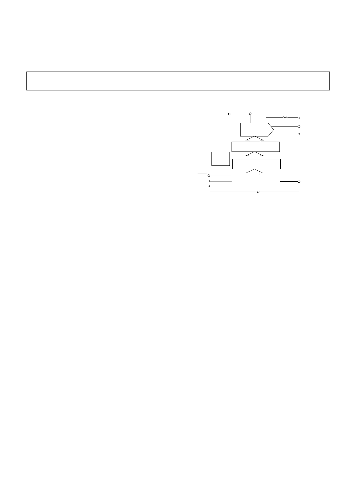
FUNCTIONAL BLOCK DIAGRAM
V
REF
12/14
BIT
R-2R DAC
DAC REGISTER
INPUT LATCH
CONTROL LOGIC &
INPUT SHIFT REGISTER
GND
R
R
FB
I
OUT1
I
OUT2
SDO
SYNC
SCLK
SDIN
AD5444/
AD5446
Power On
Reset
V
DD
GENERAL DESCRIPTION
The AD5444/5446 are CMOS 12 and 14-bit Current
Output digital-to-analog converters respectively.
These devices operate from a +2.5 V to 5.5 V power supply, making them suited to battery powered applications
and many other applications.
These DACs utilize double buffered 3-wire serial interface
that is compatible with SPI
TM
, QSPITM, MICROWIRE
TM
The applied external reference input voltage (V
mines the full scale output current. An integrated feedback
resistor (R
voltage output when combined with an external Current to
Voltage precision amplifier.
The AD5444/5446 DACs are available in small 10-lead
MSOP packages.
and most DSP interface standards.
On power-up, the internal shift register and latches are
filled with zeros and the DAC output is at zero scale.
As a result of manufacture on a CMOS sub micron
process, they offer excellent four quadrant multiplication
characteristics, with large signal multiplying bandwidths
of 10MHz.
*US Patent Number 5,689,257
SPI and QSPI are trademarks of Motorola, Inc.
MICROWIRE is a trademark of National Semiconductor Corporation.
REV. PrB Oct, 2003
Information furnished by Analog Devices is believed to be accurate and
reliable. However, no responsibility is assumed by Analog Devices for its
use, nor for any infringements of patents or other rights of third parties
which may result from its use. No license is granted by implication or
otherwise under any patent or patent rights of Analog Devices.
One Technology Way, P.O. Box 9106, Norwood, MA 02062-9106, U.S.A.
Tel: 781/329-4700 World Wide W eb Site: http://www .analog.com
Fax: 781/326-8703 Analog Devices, Inc., 2003
) deter-
REF
) provides temperature tracking and full scale
FB
Page 2

PRELIMINARY TECHNICAL DA T A
AD5444/AD5446–SPECIFICATIONS
1
(VDD = 2.5 V to 5.5 V, V
AC performance with AD8038 unless otherwise noted.)
Parameter Min Typ Max Units Conditions
STATIC PERFORMANCE
AD5444
Resolution 12 Bits
Relative Accuracy ±
Differential Nonlinearity ±
AD5446
Resolution 14 Bits
Relative Accuracy ±2 LSB
Differential Nonlinearity ±1 LSB Guaranteed Monotonic
Total Unadjusted Error ±2.44 mV
Gain Error ±1.22 mV
Gain Error Temp Coefficient
Output Leakage Current ±10 n A Data = 0000H, TA = 25°C, I
Output Voltage Compliance 1.23 V
REFERENCE INPUT
Reference Input Range ±10 V
V
Input Resistance 8 9.3 12 kΩ Input resistance TC = -50ppm/°C
REF
RFB Resistance 8 9.3 12 kΩ Input resistance TC = -50ppm/°C
Input Capacitance
Zero Code 3 6 pF
Full Scale Code 5 8 pF
DIGITAL INPUTS/OUTPUTS
Input High Voltage, V
Input Low Voltage, V
Output High Voltage, V
Output Low Voltage, V
Input Leakage Current, I
Input Capacitance 10 pF
DYNAMIC PERFORMANCE
Reference Multiplying BW 1 0 MHz V
Output Voltage Settling Time V
AD5440 40 tb d n s Measured to +/-1mV of FS
AD5447 80 tb d n s Measured to +/-1mV of FS
Digital Delay 20 40 ns Interface delay time
10% to 90% Dettling Time 10 30 ns Rise and Fall time, V
Digital to Analog Glitch Impulse
Multiplying Feedthrough Error DAC latch loaded with all 0s.
Output Capacitance
IOUT1 5 p F DAC Latches Loaded with all 0s
IOUT2 1 0 pF DAC Latches Loaded with all 0s
Digital Feedthrough 0. 1 nV -s Feedthrough to DAC output with CS high
= +10 V, I
REF
2
IH
IL
OL
x = O V. All specifications T
OUT
2
2
2.0 V VDD = 3.6 V to 5 V
1.7 V VDD = 2.5 V to 3.6 V
OH
VDD -1 V VDD = 4.5 V to 5 V, I
VDD - 0.5 V VDD = 2.5 V to 3.6 V, I
IL
2
to T
MIN
0.5
½
±5 ppm FSR/
±50 n A Data = 0000H, I
unless otherwise noted. DC performance measured with OP177,
MAX
LSB
LSB Guaranteed Monotonic
°C
OUT1
OUT1
0.8 V VDD = 2.7 V to 5.5 V
0.7 V VDD = 2.5 V to 2.7 V
SOURCE
0.4 V VDD = 4.5 V to 5 V, I
SINK
0.4 V VDD = 2.5 V to 3.6 V, I
= 200uA
SOURCE
= 200uA
= 200uA
SINK
= 200uA
1 µA
= +/-3.5V, DAC loaded all 1s
REF
= 10V, R
REF
LOAD
= 100Ω, C
LOAD
DAC latch alternately loaded with 0s and 1s.
= 10V, R
100Ω, C
LOAD
REF
= 15pF
LOAD
3 nV -s 1 LSB change around Major Carry, V
-75 dB Reference = 1MHz.
Reference = 10MHz.
10 pF DAC Latches Loaded with all 1s
5 pF DAC Latches Loaded with all 1s
and Alternate Loading of all 0s and all 1s.
= 15pF
=
=0V
REF
–2– REV. PrB
Page 3
PRELIMINARY TECHNICAL DA T A
AD5444/AD5446
(VDD = 2.5 V to 5.5 V, V
= +10 V, I
REF
x = O V. All specifications T
OUT
MIN
to T
unless otherwise noted. DC performance measured with OP177,
MAX
AC performance with AD8038 unless otherwise noted.)
Parameter Min Typ Max Units Conditions
Total Harmonic Distortion -8 0 dB V
= 3.5 V pk-pk, All 1s loaded, f = 1kHz
REF
Digital THD, Clock = 1MHz
50kHz f
OUT
75 dB
Output Noise Spectral Density 25 nV/√Hz @ 1kHz
SFDR performance (Wideband)
Update = 1MHz, V
= 3.5V
REF
Update = 1MHz
50kHz Fout 78 dB
20kHz Fout 78 dB
SFDR performance (NarrowBand) Update = 1MHz, V
= 3.5V
REF
50kHz Fout 87 dB
20kHz Fout 87 dB
Intermodulation Distortion 78 dB f1 = 20kHz, f2 = 25kHz, Update=1MHz,
V
=3.5V
REF
POWER REQUIREMENTS
Power Supply Range 2.5 5.5 V
I
DD
Power Supply Sensitivity
NOTES
1
Temperature range is as follows: Y Version: –40°C to +125°C.
2
Guaranteed by design and characterisation, not subject to production test.
Specifications subject to change without notice.
2
1 µA Logic Inputs = 0 V or V
0.001 %/% ∆VDD = ±5%
DD
TIMING CHARACTERISTICS
Parameter VDD = 4.5 V to 5.5 V VDD = 2.5 V to 5.5 V Units Conditions/Comments
f
SCLK
t
1
t
2
t
3
t
4
t
5
t
6
t
7
t
8
NOTES
1
See Figures 1. Temperature range is as follows: Y Version: –40°C to +125°C. Guaranteed by design and characterisation, not subject to
production test. All input signals are specified with tr =tf = 5ns (10% to 90% of VDD) and timed from a voltage level of (VIL + VIH)/2.
Specifications subject to change without notice.
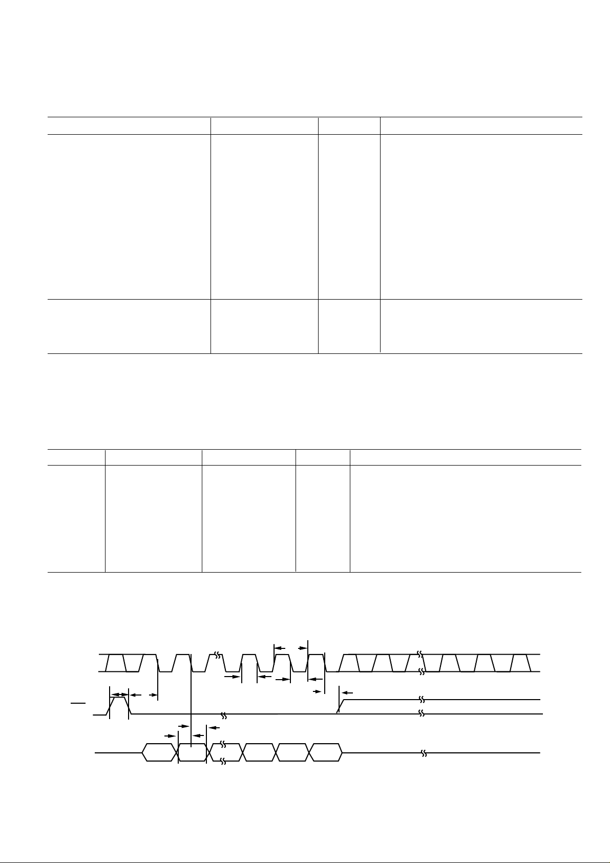
SCLK
SYNC
DIN
tba 50 MHz max Max Clock frequency
20 ns min SCLK Cycle time
8 ns min SCLK High Time
8 ns min SCLK Low Time
8 ns min
5 ns min Data Setup Time
4.5 ns min Data Hold Time
5 ns min SYNC rising edge to SCLK active edge
30 ns min Minimum SYNC high time
t
8
t
4
t
6
t
5
DB15
(V
= +5 V, I
REF
t
1
t
2
2 = O V. All specifications T
OUT
SYNC falling edge to SCLK active edge setup
t
3
DB0
t
7
MIN
to T
unless otherwise noted.)
MAX
time
1
Figure 1. Timing Diagram.
–3–REV. PrB
Page 4
AD5444/AD5446
PRELIMINARY TECHNICAL DA T A
ABSOLUTE MAXIMUM RATINGS
(TA = +25°C unless otherwise noted)
1, 2
VDD to GND –0.3 V to +7 V
V
REF, RFB
I
OUT
Logic Inputs & Output
to GND –12 V to +12 V
1 to GND –0.3 V to +7 V
3
-0.3V to VDD +0.3 V
Operating Temperature Range
Industrial (Y Version) –40°C to +125°C
Storage Temperature Range –65°C to +150°C
Junction Temperature +150°C
10 lead MSOP θ
Thermal Impedance 206°C/W
JA
Lead Temperature, Soldering (10seconds) 300°C
IR Reflow, Peak Temperature (<20 seconds) +235°C
NOTES
1
Stresses above those listed under “Absolute Maximum Ratings” may cause permanent
damage to the device. This is a stress rating only and functional operation of the device
at these or any other conditions above those listed in the operational sections of this
specification is not implied. Exposure to absolute maximum rating conditions for
extended periods may affect device reliability. Only one absolute maximum rating may
be applied at any one time.
2
Transient currents of up to 100mA will not cause SCR latchup.
3
Overvoltages at SCLK, SYNC, DIN, will be clamped by internal diodes.
ORDERING GUIDE
Model Resolution INL Temperature Range Package Description Branding Package Option
AD5444YRM 12
AD5446YRM 14
±0.5
±2
-40 oC to +125 oC MSOP RM-10
-40 oC to +125 oC MSOP RM-10
CAUTION
ESD (electrostatic discharge) sensitive device. Electrostatic charges as high as 4000 V readily
accumulate on the human body and test equipment and can discharge without detection.
Although the AD5444/5446 features proprietary ESD protection circuitry, permanent damage may
occur on devices subjected to high energy electrostatic discharges. Therefore, proper ESD precautions
are recommended to avoid performance degradation or loss of functionality.
–4– REV. PrB
Page 5
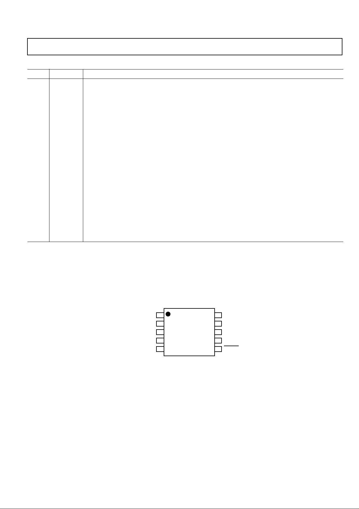
PRELIMINARY TECHNICAL DA T A
MSOP Mnemonic Function
AD5444/AD5446
PIN FUNCTION DESCRIPTION
1I
2I
1 DAC Current Output.
OUT
2 DAC Analog Ground. This pin should normally be tied to the analog ground of the system.
OUT
3 GND Ground Pin.
4 SCLK Serial Clock Input. By default, data is clocked into the input shift register on the falling edge of
the serial clock input. Alternatively, by means of the serial control bits, the device may be
configured such that data is clocked into the shift register on the rising edge of SCLK.
5 SDIN Serial Data Input. Data is clocked into the 16-bit input register on the active edge of the serial
clock input. By default, on power up, data is clocked into the shift register on the falling edge of
SCLK. The control bits allow the user to change the active edge to rising edge.
6 SYNC Active Low Control Input. This is the frame synchronization signal for the input data. When
SYNC goes low, it powers on the SCLK and DIN buffers and the input shift register is
enabled. Data is loaded to the shift register on the active edge of the following clocks.
7 SDO Serial Data Output. This allows a number of parts to be daisychained. By default, data is clocked
into the shift register on the falling edge and out via SDO on the rising edge of SCLK. Data will
always be clocked out on the alternate edge to loading data to the shift register. Writing the
Readback control word to the shift register makes the DAC register contents available for
readback on the SDO pin, clocked out on the opposite edges to the active clock edge.
8V
9V
10 R
DD
REF
FB
Positive power supply input. These parts can be operated from a supply of +2.5 V to +5.5 V.
DAC reference voltage input pin.
DAC feedback resistor pin. Establish voltage output for the DAC by connecting to external
amplifier output.
PIN CONFIGURATION
MSOP (RM-10)
GND
SDIN
1
2
3
4
5
AD5444/
AD5446
Not to Scale)
(
I
OUT1
I
OUT2
SCLK
16
15
14
13
12
RFB
VREF
VDD
SDO
SYNC
–5–REV. PrB
Page 6

PRELIMINARY TECHNICAL DA T A
AD5444/AD5446
TERMINOLOGY
Relative Accuracy
Relative accuracy or endpoint nonlinearity is a measure of the maximum deviation from a straight line passing through the
endpoints of the DAC transfer function. It is measured after adjusting for zero and full scale and is normally expressed in
LSBs or as a percentage of full scale reading.
Differential Nonlinearity
Differential nonlinearity is the difference between the measured change and the ideal 1 LSB change between any two adjacent codes. A specified differential nonlinearity of -1 LSB max over the operating temperature range ensures monotonicity.
Gain Error
Gain error or full-scale error is a measure of the output error between an ideal DAC and the actual device output. For
these DACs, ideal maximum output is V
tance.
Output Leakage Current
Output leakage current is current which flows in the DAC ladder switches when these are turned off. For the I
nal, it can be measured by loading all 0s to the DAC and measuring the I
line when the DAC is loaded with all 1s
I
OUT2
Output Capacitance
Capacitance from I
OUT1
or I
to AGND.
OUT2
Output Current Settling Time
This is the amount of time it takes for the output to settle to a specified level for a full scale input change. For these devices, it is specifed with a 100 Ω resistor to ground. The settling time specification includes the digital delay from SYNC
rising edge to the full scale output change.
Digital to Analog Glitch lmpulse
The amount of charge injected from the digital inputs to the analog output when the inputs change state. This is normally
specified as the area of the glitch in either pA-secs or nV-secs depending upon whether the glitch is measured as a current
or voltage signal.
Digital Feedthrough
When the device is not selected, high frequency logic activity on the device digital inputs may be capacitivelly coupled
through the device to show up as noise on the I
feedthrough.
Multiplying Feedthrough Error
This is the error due to capacitive feedthrough from the DAC reference input to the DAC I
loaded to the DAC.
Total Harmonic Distortion (THD)
The DAC is driven by an ac reference. The ratio of the rms sum of the harmonics of the DAC output to the fundamental
value is the THD. Usually only the lower order harmonices are included, such as second to fifth.
2
2
2
THD
= 20log √(V
V
2
+ V
3
+ V
1
4
+ V
2
)
5
Digital Intermodulation Distortion
Second order intermodulation (IMD) measurements are the relative magnitudes of the fa and fb tones generated digitally
by the DAC and the second order products at 2fa-fb and 2fb-fa.
Compliance Voltage Range
The maximum range of (output) terminal voltage for which the device will provide the specified characteristics.
Spurious-Free Dynamic Range(SFDR)
It is the usable dynamic range of a DAC before spurious noise interferes or distorts the fundamental signal. SFDR is the
measure of difference in amplitude between the fundamental and the largest harmonically or nonharmonically related spur
from dc to full Nyquist bandwidth (half the DAC sampling rate or fs/2). Narrow band SFDR is a measure of SFDR over
an arbitrary window size, in this case 50% of hte fundamental. Digital SFDR is a measure of the usable dymanic range of
the DAC when the signal is a digitally generated sine wave.
– 1 LSB. Gain error of the DACs is adjustable to zero with external resis-
REF
termi-
current. Minimum current will flow in the
OUT1
pins and subsequently into the following circuitry. This noise is digital
OUT
terminal, when all 0s are
OUT1
OUT1
–6– REV. PrB
Page 7

PRELIMINARY TECHNICAL DA T A
Typical Performance Characteristics
TPC 1. INL vs. Code (12-Bit DAC)
TPC 2. INL vs. Code (14-Bit DAC)
AD5444/AD5446
TPC 3. DNL vs. Code (12-Bit DAC)
TPC 4. DNL vs. Code (14-Bit DAC)
TPC 7. DNL vs. Reference Voltage
TPC 5. INL vs Reference Voltage
TPC 8. DNL vs Code - Biased Mode
TPC 6. DNL vs. Code (10-Bit DAC)
TPC 9. TUE vs Code
–7–REV. PrB
Page 8

AD5444/AD5446
PRELIMINARY TECHNICAL DA T A
TPC10. Linearity Errors vs. V
TPC 13. DNL Error vs. Reference -
Biased Mode
DD
TPC11. INL vs Code - Biased Mode
TPC 14. Supply Current vs. Clock Freq
TPC 12. INL Error vs. Reference -
Biased Mode
TPC 15. Logic Threshold vs Supply
Voltage
TPC 16.
TPC 17.
–8– REV. PrB
TPC 18
Page 9

PRELIMINARY TECHNICAL DA T A
AD5444/AD5446
TPC 19. Supply Current vs Logic Input
Voltage
TPC 22. Reference Multiplying
Bandwidth - small signal
TPC 20. Reference Multiplying
Bandwidth - small signal
TPC 23. Reference Multiplying
Bandwidth - large signal
TPC 21. Reference Multiplying
Bandwidth - large signal
TPC 24. Settling Time
TPC 25. Midscale Transition and
Digital Feedthrough
TPC 26. Power Supply Rejection vs
Frequency
–9–REV. PrB
TPC 27. Noise Spectral Density vs
Frequency
Page 10

AD5444/AD5446
PRELIMINARY TECHNICAL DA T A
GENERAL DESCRIPTION
DAC SECTION
The AD5444 and AD5446 are 12 and 14 bit current output DACs consisting of a segmented (4-Bits) inverting R2R ladder configuration.
The feedback resistor R
has a value of R. The value of R
FB
is typically 9.3kΩ (minimum 8kΩ and maximum 12kΩ).
If I
is kept at the same potential as GND, a constant
OUT1
current flows in each ladder leg, regardless of digital input
code. Therefore, the input resistance presented at V
REF
is
always constant and nominally of value R. The DAC output (I
) is code-dependent, producing various resis-
OUT
tances and capacitances. External amplifier choice should
take into account the variation in impedance generated by
the DAC on the amplifiers inverting input node.
Access is provided to the V
, RFB, and I
REF
terminals
OUT1
of the DAC, making the device extremely versatile and
allowing it to be configured in several different operating
modes, for example, to provide a unipolar output and in
four quadrant multiplication in bipolar mode. Note that a
matching switch is used in series with the internal R
FB
feedback resistor. If users attempt to measure RFB, power
must be applied to V
to achieve continuity.
DD
SERIAL INTERFACE
The AD5444/5446 have an easy to use 3-wire interface
which is compatible with SPI/QSPI/MicroWire and DSP
interface standards. Data is written to the device in 16 bit
words. This 16-bit word consists of 2 control bits and
either 12 or 14 data bits as shown in Figure 2. The
AD5446 uses all 14 bits of DAC data. The AD5444 uses
twelve bits and ignores the two LSBs.
DAC Control Bits C1, C0
Control bits C1 and C0 the user to load and update the
new DAC code and to change the active clock edge. By
default the shift register clocks data in on the falling edge,
this can be changed via the control bits. In this case, the
DAC core is inoperative until the next data frame. A
power cycle resets this back to default condition.
On chip power on reset circuitry ensures the device
powers on with zeroscale loaded to the DAC register and
line.
I
OUT
TABLE III. DAC CONTROL BITS
C1 C0 Funtion Implemented
0 0 Load and Update(Power On Default)
0 1 Reserved
1 0 Reserved
1 1 Clock Data to shift register On Rising Edge
SYNCSYNC
SYNC Function
SYNCSYNC
SYNC is an edge-triggered input that acts as a frame
synchronization signal and chip enable. Data can only be
transferred into the device while SYNC is low. To start
the serial data transfer, SYNC should be taken low observing the minimum SYNC falling to SCLK falling
edge setup time, t
.
4
After the falling edge of the 16th SCLK pulse, bring
SYNC high to transfer data from the input shift register to
the DAC register.
CIRCUIT OPERATION
Unipolar Mode
Using a single op amp, these devices can easily be
configured to provide 2 quadrant multiplying operation or
a unipolar output voltage swing as shown in Figure 3.
When an output amplifier is connected in unipolar mode,
the output voltage is given by:
V
= -D/2n x V
OUT
REF
Where D is the fractional representation of the digital
word loaded to the DAC, and n is the number of bits.
D= 0 to 4095 (12-Bit AD5444)
= 0 to 16383 (14-Bit AD5446)
Note that the output voltage polarity is opposite to the
V
polarity for dc reference voltages.
REF
DB15 (MSB)
C1 C0
CONTROL BITS
DB11 DB10
DB9
DB8
DB7 DB6 DB5 DB4
DB3 DB2
DATA BITS
Figure 2a. AD5444 12 bit Input Shift Register Contents
DB15 (MSB)
C1 C0
CONTROL BITS
DB13 DB12
DB11
DB10
DB9 DB8 DB7 DB6
DB5 DB4
DATA BITS
Figure 2b. AD5446 14 bit Input Shift Register Contents
–10– REV. PrB
DB1
DB3
DB0
DB2
DB0 (LSB)
X
DB0 (LSB)
DB1
DB0
X
Page 11

PRELIMINARY TECHNICAL DA T A
V
DD
V
DD
V
REF
NOTES:
1
R1 AND R2 USED ONLY IF GAIN ADJUSTMENT IS REQUIRED.
2
C1 PHASE COMPENSATION (1pF - 5pF) MAY BE REQUIRED
IF A1 IS A HIGH SPEED AMPLIFIER.
V
AD5450/1/2/3
REF
R
1
SYNC
SCLK SDIN
uController
Figure 3. Unipolar Operation
These DACs are designed to operate with either negative
or positive reference voltages. The V
used by the internal digital logic to drive the DAC
switches’ ON and OFF states.
These DACs are also designed to accommodate ac reference input signals in the range of -10V to +10V.
With a fixed 10 V reference, the circuit shown above will
give an unipolar 0V to -10V output voltage swing. When
V
is an ac signal, the circuit performs two-quadrant
IN
multiplication.
The following table shows the relationship between digital
code and expected output voltage for unipolar operation.
(AD5444, 12-Bit device).
Table I. Unipolar Code Table
Digital Input Analog Output (V)
1111 1111 1111 -V
1000 0000 0000 -V
0000 0000 0001 -V
0000 0000 0000 -V
REF
REF
REF
REF
R
2
C
RFB
IOUT1
GND
1
A1
AGND
power pin is only
DD
(4095/4096)
(2048/4096) = -V
(1/4096)
(0/4096) = 0
V
REF
OUT
/2
= 0 to -V
REF
AD5444/AD5446
Bipolar Operation
In some applications, it may be necessary to generate full
4-Quadrant multplying operation or a bipolar output
swing. This can be easily accomplished by using another
external amplifier and some external resistors as shown in
Figure 4. In this circuit, the second amplifier A2 provides
a gain of 2. Biasing the external amplifier with an offset
from the reference voltage results in full 4-quadrant
multiplying operation. The transfer function of this circuit
shows that both negative and positive output voltages are
created as the input data (D) is incremented from code
OUT
= - V
OUT
= + V
OUT
= (V
zero (V
scale (V
V
Where D is the fractional representation of the digital
word loaded to the DAC and n is the resolution of the
DAC.
D= 0 to 4095 (12-Bit AD5444)
= 0 to 16383 (14-Bit AD5446)
When V
is an ac signal, the circuit performs four-
IN
quadrant multiplication.
Table II. shows the relationship between digital code and
the expected output voltage for bipolar operation
(AD5444, 12-Bit device).
Digital Input Analog Output (V)
1111 1111 1111 +V
1000 0000 0000 0
0000 0000 0001 -V
0000 0000 0000 -V
Stability
In the I-to-V configuration, the I
inverting node of the op amp must be connected as close
as possible, and proper PCB layout techniques must be
employed. Since every code change corresponds to a step
function, gain peaking may occur if the op amp has
limited GBP and there is excessive parasitic capacitance at
the inverting node. This parasitic capacitance introduces a
pole into the open loop response which can cause ringing
or instability in the closed loop applications circuit.
) to midscale (V
REF
).
REF
x D / 2
REF
n-1
)
- VREF
- 0V ) to full
OUT
Table II. Bipolar Code Table
(2047/2048)
REF
(2047/2048)
REF
(0/2048)
REF
of the DAC and the
OUT
V
REF
± 10V
R3
20kΩ
R2
C1
RFB
IOUT1
GND
NOTES:
1
R1 AND R2 ARE USED ONLY IF GAIN ADJUSTMENT IS REQUIRED.
ADJUST R1 FOR V
2
MATCHING AND TRACKING IS ESSENTIAL FOR RESISTOR PAIRS
R3 AND R4.
3
C1 PHASE COMPENSATION (1pF-5pF) MAY BE REQUIRED
IF A1/A2 IS A HIGH SPEED AMPLIFIER.
A1
AGND
= 0V WITH CODE 10000000 LOADED TO DAC.
OUT
R4
10kΩ
R1
V
REF
SYNC
uController
V
DD
V
DD
AD5450/1/2/3
SCLK SDIN
Figure 4. Bipolar Operation (4 Quadrant Multiplication)
–11–REV. PrB
R5
20kΩ
A2
V
= -V
REF
to +V
REF
OUT
Page 12

PRELIMINARY TECHNICAL DA T A
AD5444/AD5446
An optional compensation capacitor, C1 can be added in
parallel with R
Too small a value of C1 can produce ringing at the
output, while too large a value can adversely affect the
settling time. C1 should be found empirically but 1-2pF is
generally adequate for the compensation.
SINGLE SUPPLY APPLICATIONS
Voltage Switching Mode of Operation
Figure 5 shows these DACs operating in the voltageswitching mode. The reference voltage, V
the I
OUT1
pin, I
output voltage is available at the V
configuration, a positive reference voltage results in a
positive output voltage making single supply operation
possible. The output from the DAC is voltage at a
constant impedance (the DAC ladder resistance). Thus an
op-amp is necessary to buffer the output voltage. The
reference input no longer sees a constant input impedance,
but one that varies with code. So, the voltage input should
be driven from a low impedance source.
V
IN
for stability as shown in figures 3 and 4.
FB
is applied to
is connected to AGND and the
OUT2
V
DD
RFB
V
DD
IOUT1
GND
NOTES:
1
ADDITIONAL PINS OMITTED FOR CLARITY
2
C1 PHASE COMPENSATION (1pF-5pF) MAY BE REQUIRED
IF A1 IS A HIGH SPEED AMPLIFIER.
V
REF
IN
terminal. In this
REF
R
R
1
2
V
OUT
V
= 5V
REF
DD
V
GND
C
RFB
DD
IOUT1
IOUT2
1
1/2 AD8552
V
OUT = 0 to +2.5V
ADR03
V
V
IN
OUT
GND
+
5V
-2.5V
V
1/2 AD8552
-
5V
NOTES:
1
ADDITIONAL PINS OMITTED FOR CLARITY
2
C1 PHASE COMPENSATION (1pF-5pF) MAY BE REQUIRED
IF A1 IS A HIGH SPEED AMPLIFIER.
Figure 6. Positive Voltage output with minimum of
components.
ADDING GAIN
In applications where the output voltage is required to be
greater than V
, gain can be added with an additional
IN
external amplifier or it can also be achieved in a single
stage. It is important to take into consideration the effect
of temperature coefficients of the thin film resistors of the
DAC. Simply placing a resistor in series with the RFB
resistor will causing mis-matches in the Temperature
coefficients resulting in larger gain temperature coefficient
errors. Instead, the circuit of Figure 7 is a recommended
method of increasing the gain of the circuit. R1, R2 and
R3 should all have similar temperature coefficients, but
they need not match the temperature coefficients of the
DAC. This approach is recommended in circuits where
gains of great than 1 are required.
Figure 5. Single Supply Voltage Switching Mode Operation.
It is important to note that VIN is limited to low voltages
because the switches in the DAC ladder no longer have
the same source-drain drive voltage. As a result their on
resistance differs and this degrades the integral linearity of
the DAC. Also, VIN must not go negative by more than
0.3V or an internal diode will turn on, exceeding the max
ratings of the device. In this type of application, the full
range of multiplying capability of the DAC is lost.
POSITIVE OUTPUT VOLTAGE
Note that the output voltage polarity is opposite to the
V
polarity for dc reference voltages. In order to achieve
REF
a positive voltage output, an applied negative reference to
the input of the DAC is preferred over the output
inversion through an inverting amplifier because of the
resistors tolerance errors. To generate a negative
reference, the reference can be level shifted by an op amp
such that the V
and GND pins of the reference
OUT
become the virtual ground and -2.5V respectively as
shown in Figure 6.
V
DD
C
R
2
V
IN
NOTES:
1
ADDITIONAL PINS OMITTED FOR CLARITY
2
C1 PHASE COMPENSATION (1pF-5pF) MAY BE REQUIRED
IF A1 IS A HIGH SPEED AMPLIFIER.
V
V
REF
GND
RFB
DD
IOUT1
IOUT2
1
V
OUT
R
3
GAIN = R2 + R3
R
2
R2
R1 = R2R3
R2 + R3
Figure 7. Increasing Gain of Current Output DAC
USED AS A DIVIDER OR PROGRAMMABLE GAIN
ELEMENT
Current Steering DACs are very flexible and lend
themselves to many different applications. If this type of
DAC is connected as the feedback element of an op-amp
and R
then the output voltage is inversely proportional to the
digital input fraction D. For D = 1-2
is used as the input resistor as shown in Figure 8,
FB
n
the output voltage
is
–12– REV. PrB
Page 13

PRELIMINARY TECHNICAL DA T A
AD5444/AD5446
V
OUT
= -V
IN
V
IN
/D = -V
IN
V
/(1-2-n)
DD
error source can be minimized. Table IV. suggests some
of the suitable dc references available from Analog
Devices that are suitable for use with this range of current
output DACs.
RFB
V
DD
V
IOUT1
GND
NOTES:
1
ADDITIONAL PINS OMITTED FOR CLARITY
REF
V
OUT
Figure 8. Current Steering DAC used as a divider or
Programmable Gain Element
As D is reduced, the output voltage increases. For small
values of the digital fraction D, it is important to ensure
that the arnplifier does not saturate and also that the
required accuracy is met. For example, an eight bit DAC
driven with the binary code 10H (00010000), i.e., 16
decimal, in the circuit of Figure 8 should cause the output
voltage to be sixteen times V
. However, if the DAC has
IN
a linearity specification of +/- 0.5LSB then D
can in fact have the weight anywhere in the range 15.5/256
to 16.5/256 so that the possible output voltage will be in
the range 15.5V
to 16.5VIN—an error of + 3% even
IN
though the DAC itself has a maximum error of 0.2%.
DAC leakage current is also a potential error source in
divider circuits. The leakage current must be
counterbalanced by an opposite current supplied from the
op amp through the DAC. Since only a fraction D of the
current into the V
terminal is routed to the I
REF
OUT1
ter-
minal, the output voltage has to change as follows:
Output Error Voltage Due to Dac Leakage
= (Leakage x R)/D
where R is the DAC resistance at the V
terminal. For a
REF
DAC leakage current of 10nA, R = 10 kilohm and a gain
(i.e., 1/D) of 16 the error voltage is 1.6mV.
AMPLIFIER SELECTION
The primary requirement for the current-steering mode is
an amplifier with low input bias currents and low input
offset voltage. The input offset voltage of an op amp is
multiplied by the variable gain (due to the code dependent
output resistance of the DAC) of the circuit. A change in
this noise gain between two adjacent digital fractions
produces a step change in the output voltage due to the
amplifier’s input offset voltage. This output voltage
change is superimposed upon the desired change in output
between the two codes and gives rise to a differential
linearity error, which if large enough could cause the
DAC to be non-monotonic.
The input bias curent of an op amp also generates an
offset at the voltage output as a result of the bias current
flowing in the feedback resistor R
. Most op amps have
FB
input bias currents low enough to prevent any significant
errors in 12-Bit applications, however for 14-Bit
applications some consideration should be given to
selecting an appropriate amplifier.
Common mode rejection of the op amp is important in
voltage switching circuits, since it produces a code
dependent error at the voltage output of the circuit. Most
op amps have adequate common mode rejection for use at
8-, 10- and 12-Bit resolution.
Provided the DAC switches are driven from true wideband
low impedance sources (V
and AGND) they settle
IN
quickly. Consequently, the slew rate and settling time of a
voltage switching DAC circuit is determined largely by
the output op amp. To obtain minimum settling time in
this configuration, it is important to minimize capacitance
at the V
node (voltage output node in this application)
REF
of the DAC. This is done by using low inputs capacitance
buffer amplifiers and careful board design.
Most single supply circuits include ground as part of the
analog signal range, which in turns requires an
ampliferthat can handle rail to rail signals, there is a large
range of single supply amplifiers available from Analog
Devices.
REFERENCE SELECTION
When selecting a reference for use with the AD5426 series
of current output DACs, pay attention to the references
output voltage temperature coefficient specification. This
parameter not only affects the full scale error, but can also
affect the linearity (INL and DNL) performance. The
reference temperature coefficient should be consistent with
the system accuracy specifications. For example, an 8-bit
system required to hold its overall specification to within
1LSB over the temperature range 0-50
maximum system drift with temperature should be less than
78ppm/
range to overall specification within 2LSBs requires a
maximum drift of 10ppm/
o
C. A 14-Bit system with the same temperature
o
C. By choosing a precision
o
C dictates that the
reference with low output temperature coefficient this
–13–REV. PrB
PCB LAYOUT AND POWER SUPPLY DECOUPLING
In any circuit where accuracy is important, careful
consideration of the power supply and ground return
layout helps to ensure the rated performance. The printed
circuit board on which the AD5426/AD5432/AD5443 is
mounted should be designed so that the analog and digital
sections are separated, and cofined to certain areas of the
board. If the DAC is in a system where multiple devices
require an AGND-to-DGND connection, the connection
should be made at one point only. The star ground point
should be established as close as possible to the device.
These DACs should have ample supply bypassing of 10
µF in parallel with 0.1 µF on the supply located as close
to the package as possible, ideally right up against the
device. The 0.1 µF capacitor should have low Effective
Page 14

PRELIMINARY TECHNICAL DA T A
AD5444/AD5446
Table IV. Listing of suitable ADI Precision References recommended for use with these DACs.
Reference Output Voltage Initial Tolerance Temperature Drift 0.1Hz to 10Hz noise Package
ADR01 10 V 0.1% 3ppm/oC20µVp-p SC70, TSOT, SOIC
ADR02 5 V 0.1% 3ppm/
ADR03 2.5 V 0.2% 3ppm/
ADR425 5 V 0.04% 3ppm/oC 3.4µVp-p MSOP, SOIC
Table V. Listing of some precision ADI Op Amps suitable for use with these DACs.
o
C10µVp-p SC70, TSOT, SOIC
o
C10µVp-p SC70, TSOT, SOIC
Part # Max Supply Voltage V VOS(max)
OP97
OP1177
±
20 25 0.1 0.9 0.2
±
18 60 2 1.3 0.7
µµ
µVIB(max) nA GBP MHz Slew Rate V/
µµ
µµ
µs
µµ
AD8551 ±6 5 0.05 1.5 0.4
Table VI. Listing of some High Speed ADI Op Amps suitable for use with these DACs.
Part # Max Supply Voltage V BW @ ACL MHz Slew Rate V/
µµ
µsVOS(max)
µµ
µµ
µVI
µµ
(max) nA
B
AD8065 ±12 145 180 1500 0.01
AD8021 ±12 200 100 1000 1000
AD8038 ±5 350 425 3000 0.75
AD9631 ±5 320 1300 10000 7000
Series Resistance (ESR) and Effective Series Inductance
(ESI), like the common ceramic types that provide a low
impedance path to ground at high frequencies, to handle
transient currents due to internal logic switching. Low
ESR 1 µF to 10 µF tantalum or electrolytic capacitors
should also be applied at the supplies to minimize
transient disturbance and filter out low frequency ripple.
Fast switching signals such as clocks should be shielded
with digital ground to avoid radiating noise to other parts
of the board, and should never be run near the reference
inputs.
Avoid crossover of digital and analog signals. Traces on
opposite sides of the board should run at right angles to
each other. This reduces the effects of feedthrough
through the board. A microstrip technique is by far the
best, but not always possible with a doublesided board. In
this technique, the component side of the board is
dedicated to ground plane while signal traces are placed
on the solder side.
It is good practice to employ compact, minimum lead
length PCB layout design. Leads to the input should be as
short as possible to minimize IR drops and stray
inductance.
The PCB metal traces between V
and RFB should also
REF
be matched to minimize gain error. To maximize on high
frequency performance, the I-to-V amplifier should be
located as close to the device as possible.
–14– REV. PrB
Page 15

PRELIMINARY TECHNICAL DA T A
Overview of AD54xx devices
AD5444/AD5446
Part # Resolution #DACs IN L t
AD5403182
±0.25
20ns Parallel CP-40 10 MHz BW, 17 ns CS Pulse Width, 4-
Interface Package Features
S
Quadrant Multiplying Resistors
AD5410181
±0.25
20ns Serial RU -16 10 MHz BW, 50 MHz Serial, 4- Quadrant
Multiplying Resistors
AD5413182
±0.25
20ns Serial RU -24 10 MHz BW, 50 MHz Serial, 4- Quadrant
Multiplying Resistors
AD5424 8 1
AD5425 8 1
AD5426 8 1
AD5428282
AD5429282
AD5450281
AD5404110 2
±0.25
±0.25
±0.25
±0.25
±0.25
±0.25
±0.5
60ns Parallel RU-16, CP-20 10 MHz BW, 17 ns CS Pulse Width
100ns Serial RM-10 Byte Load,10 MHz BW, 50 MHz Serial
100ns Serial RM-10 10 MHz BW, 50 MHz Serial
60ns Parallel RU-2 0 10 MHz BW, 17 ns CS Pulse Width
100ns Serial RU-10 10 MHz BW, 50 MHz Serial
100ns Serial RJ-8 10 MHz BW, 50 MHz Serial
25ns Parallel CP-40 10 MHz BW, 17 ns CS Pulse Width, 4-
Quadrant Multiplying Resistors
AD5411110 1
±0.5
25ns Serial RU -16 10 MHz BW, 50 MHz Serial, 4- Quadrant
Multiplying Resistors
AD5414110 2
±0.5
25ns Serial RU -24 10 MHz BW, 50 MHz Serial, 4- Quadrant
Multiplying Resistors
AD5432 10 1
AD5433 10 1
AD5439210 2
AD5440210 2
AD5451210 1
±0.5
±0.5
±0.5
±0.5
±0.25
110ns Serial RM-10 10 MHz BW, 50 MHz Serial
70ns Parallel RU-20, CP-20 10 MHz BW, 17 ns CS Pulse Width
110ns Serial RU-16 10 MHz BW, 50 MHz Serial
70ns Parallel RU-2 4 10 MHz BW, 17 ns CS Pulse Width
110ns Serial RJ-8 10 MHz BW, 50 MHz Serial
AD540521 2 2 ±1 120ns Parallel CP-40 10 MHz BW, 17 ns CS Pulse Width, 4-
Quadrant Multiplying Resistors
AD5412112 1
±1
160ns Serial RU-16 10 MHz BW, 50 MHz Serial, 4- Quadrant
Multiplying Resistors
AD5415212 2
±1
160ns Serial RU-24 10 MHz BW, 50 MHz Serial, 4- Quadrant
Multiplying Resistors
AD5443 12 1 ± 1 160ns Serial RM-10 10 MHz BW, 50 MHz Serial
AD5445 12 1 ± 1 120ns Parallel RU-20, CP-20 10 MHz BW, 17 ns CS Pulse Width
AD544721 2 2 ±1 120ns Parallel R U-2 4 10 MHz BW, 17 ns CS Pulse Width
AD544921 2 2 ±1 160ns Serial RU-16 10 MHz BW, 50 MHz Serial
AD5452212 1
AD5453214 1
1
Future parts, contact factory for availability
2
In development, contact factory for availability
±0.5
±2
160ns Serial RJ-8, RM-8 10 MHz BW, 50 MHz Serial
180ns Serial RJ-8, RM-8 10 MHz BW, 50 MHz Serial
0.122 (3.10)
0.114 (2.90)
0.006 (0.15)
0.002 (0.05)
SEATING
OUTLINE DIMENSIONS
Dimensions shown in inches and (mm).
8 Lead MSOP
(RM-8)
0.122 (3.10)
0.114 (2.90)
5
8
1
PIN 1
0.0256 (0.65) BSC
0.120 (3.05)
0.112 (2.84)
0.018 (0.46)
0.008 (0.20)
PLANE
0.199 (5.05)
0.187 (4.75)
4
0.043 (1.09)
0.037 (0.94)
0.011 (0.28)
0.003 (0.08)
–15–REV. PrB
0.120 (3.05)
0.112 (2.84)
33
27
0.028 (0.71)
0.016 (0.41)
 Loading...