

Page 1
Real-Time Analog
V
FEATURES
VO = VY(VZ/VX)m transfer function
Wide dynamic range (denominator) −1000:1
Simultaneous multiplication and division
Resistor-programmable powers and roots
No external trims required
Low input offsets <100 μV
Low error ±0.25% of reading (100:1 range)
Monolithic construction
Real-time analog multiplication, division and
exponentiation
High accuracy analog division with a wide input dynamic range
On board +2 V or +10 V scaling reference
Voltage and current (summing) input modes
Monolithic construction with lower cost and higher
reliability than hybrid and modular circuits
APPLICATIONS
One- or two-quadrant multiply/divide
Log ratio computation
Squaring/square rooting
Trigonometric function approximations
Linearization via curve fitting
Precision AGC
Power functions
Computational Unit (ACU)
AD538
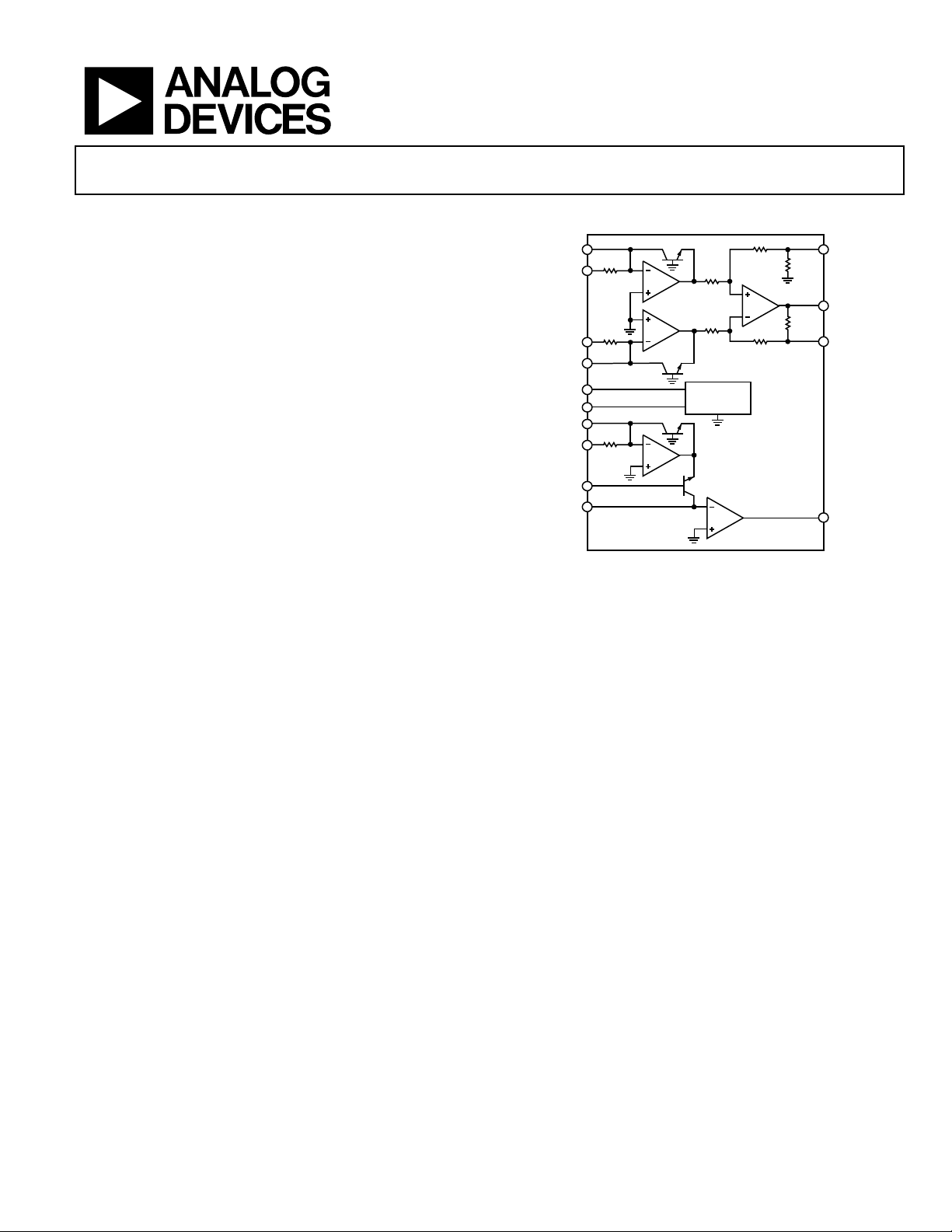
FUNCTIONAL BLOCK DIAGRAM
+10
+2V
I
X
25kΩ
V
X
LOG
RATIO
25kΩ
V
Z
I
Z
INTERNAL
VO LTAG E
REFERENCE
V
Y
25kΩ
I
Y
C
I
LOG
ANTILOG
Figure 1.
100Ω
AD538
OUTPUT
100Ω
D
B
A
V
O
00959-001
GENERAL DESCRIPTION
The AD538 is a monolithic real-time computational circuit
that provides precision analog multiplication, division, and
exponentiation. The combination of low input and output offset
voltages and excellent linearity results in accurate computation
over an unusually wide input dynamic range. Laser wafer
trimming makes multiplication and division with errors as low
as 0.25% of reading possible, while typical output offsets of
100 μV or less add to the overall off-the-shelf performance level.
Real-time analog signal processing is further enhanced by the
400 kHz bandwidth of the device.
The overall transfer function of the AD538 is V
Programming a particular function is via pin strapping. No
external components are required for one-quadrant (positive
input) multiplication and division. Two-quadrant (bipolar
numerator) division is possible with the use of external level
shifting and scaling resistors. The desired scale factor for both
Rev. E
Information furnished by Analog Devices is believed to be accurate and reliable. However, no
responsibility is assumed by Analog Devices for its use, nor for any infringements of patents or other
rights of third parties that may result from its use. Specifications subject to change without notice. No
license is granted by implication or otherwise under any patent or patent rights of Analog Devices.
Trademarks and registered trademarks are the property of their respective owners.
= VY(VZ/VX)m.
O
multiplication and division can be set using the on-chip +2 V or
+10 V references, or controlled externally to provide simultaneous
multiplication and division. Exponentiation with an m value
from 0.2 to 5 can be implemented with the addition of one or
two external resistors.
Direct log ratio computation is possible by using only the log
ratio and output sections of the chip. Access to the multiple
summing junctions adds further to the flexibility of the AD538.
Finally, a wide power supply range of ±4.5 V to ±18 V allows
operation from standard ±5 V, ±12 V and ±15 V supplies.
The AD538 is available in two accuracy grades (A and B) over
the industrial (−25°C to +85°C) temperature range and one
grade (S) over the military (−55°C to +125°C) temperature
range. The device is packaged in an 18-lead TO-118 hermetic
side-brazed ceramic DIP. A-grade chips are also available.
One Technology Way, P.O. Box 9106, Norwood, MA 02062-9106, U.S.A.
Tel: 781.329.4700 www.analog.com
Fax: 781.461.3113 ©2011 Analog Devices, Inc. All rights reserved.
 Loading...