

Page 1
40-Channel, 14-Bit, Parallel and
Serial Input, Bipolar Voltage-Output DAC
FEATURES
40-channel DAC in 13 mm × 13 mm 108-lead CSPBGA
Guaranteed monotonic to 14 bits
Buffered voltage outputs
Output voltage span of 3.5 V × V
Maximum output voltage span of 17.5 V
System calibration function allowing user-programmable
offset and gain
Pseudo differential outputs relative to REFGND
Clear function to user-defined REFGND (
Simultaneous update of DAC outputs (
DAC increment/decrement mode
Channel grouping and addressing features
V
CCVDDVSS
POWER-ON
RESET
RESET
FIFOEN
DCEN/WR
SYNC/CS
REG0
REG1
DB13
SCLK/DB12
DIN/DB11
DB0
A7
A0
SER/PAR
DIN
SCLK
SDO
REFGND B1
REFGND B2
REFGND C1
REFGND C2
REFGND D1
REFGND D2
AD5379—Protected by U.S. Patent No. 5,969,657; other patents pending.
Rev. A
Information furnished by Analog Devices is believed to be accurate and reliable.
However, no responsibility is assumed by Analog Devices for its use, nor for any
infringements of patents or other rights of third parties that may result from its use.
Specifications subject to change without notice. No license is granted by implication
or otherwise under any patent or patent rights of Analog Devices. Trademarks and
registered trademarks are the property of their respective owners.
INTERFACE
BUSY
FIFOSTATE MACHINE
14
/
(+)
REF
CLR
pin)
LDAC
pin)
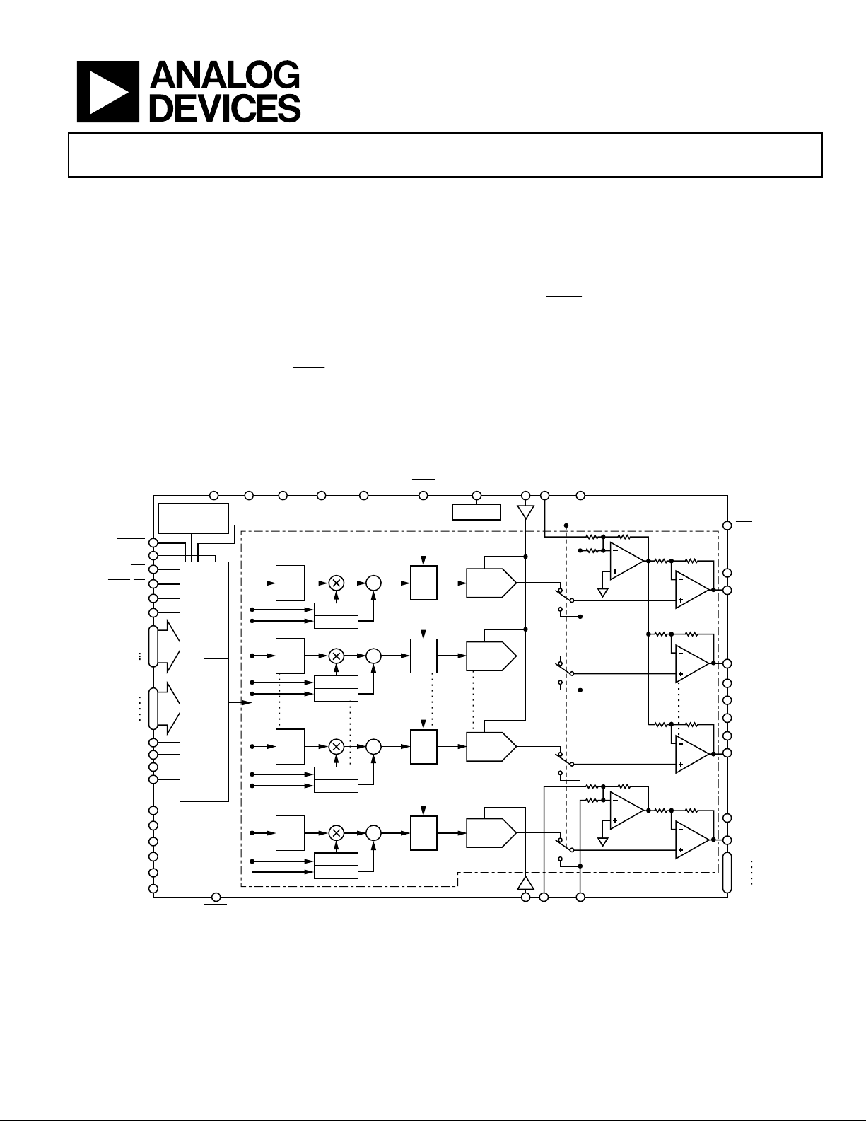
FUNCTIONAL BLOCK DIAGRAM
AGND
INPUT
REG
0–1
14
INPUT
REG
2
14
INPUT
REG
7
14
INPUT
REG
8–9
14
14
/
14
/
14
/
14
/
14
/
14
/
14
/
14
/
DGND LDAC V
AD5379
/
m REG0–1
c REG0–1
/
m REG2
c REG2
/
m REG7
c REG7
/
m REG8–9
c REG8–9
14
14
14
14
/
/
/
/
DAC
REG
0–1
DAC
REG
2
DAC
REG
7
DAC
REG
8–9
Figure 1.
Interface options:
Parallel interface
DSP/microcontroller-compatible, 3-wire serial interface
2.5 V to 5.5 V JEDEC-compliant digital levels
SDO daisy-chaining option
Power-on reset
RESET
Digital reset (
pin and soft reset function)
APPLICATIONS
Level setting in automatic test equipment (ATE)
Variable optical attenuators (VOA)
Optical switches
Industrial control systems
1(+) V
1(–) REFGND A1
REF
14
14
14
14
VBIAS
/
/
/
/
BIASVREF
DAC 0–1
DAC 2
DAC 7
DAC 8–9
×4
V
2(+) V
REF
One Technology Way, P.O. Box 9106, Norwood, MA 02062-9106, U.S.A.
Tel: 781.329.4700
Fax: 781.326.8703 © 2005 Analog Devices, Inc. All rights reserved.
2(–) REFGND A2
REF
www.analog.com
AD5379
CLR
VOUT0
VOUT1
VOUT2
VOUT3
VOUT4
VOUT5
VOUT6
VOUT7
VOUT8
VOUT9
VOUT10
VOUT39
03165-001
Page 2

AD5379
TABLE OF CONTENTS
General Description......................................................................... 3
Clear Function ............................................................................ 20
Specifications..................................................................................... 4
AC Characteristics........................................................................ 5
Timing Characteristics..................................................................... 6
Serial Interface.............................................................................. 6
Parallel Interface ........................................................................... 9
Absolute Maximum Ratings.......................................................... 11
ESD Caution................................................................................ 11
Pin Configuration and Function Descriptions........................... 12
Te r mi n ol o g y ....................................................................................15
Typical Performance Characteristics ........................................... 16
Functional Description .................................................................. 18
DAC Architecture—General..................................................... 18
Channel Groups.......................................................................... 18
Transfe r Fu nc tion ....................................................................... 18
V
Function ............................................................................. 19
BIAS
BUSY
FIFO vs. Non-FIFO Operation................................................. 21
BUSY
Power-On Reset Function ......................................................... 21
RESET
Increment/Decrement Function .............................................. 21
Interfaces.......................................................................................... 22
Parallel Interface ......................................................................... 22
Serial Interface............................................................................ 22
Data Decoding................................................................................ 24
Address Decoding .......................................................................... 25
Power Supply Decoupling ............................................................. 26
Power-On .................................................................................... 26
Typical Application Ci rc u it ........................................................... 27
Outline Dimensions ....................................................................... 28
LDAC
and
Input Function ................................................................ 21
Input Function .............................................................. 21
Functions...................................................... 20
Reference Selection .................................................................... 19
Calibration................................................................................... 20
REVISION HISTORY
1/05 — Rev. 0 to Rev. A
Changes to Table 1............................................................................ 3
Change to Transfer Function Equation ....................................... 18
4/04 — Revision 0: Initial Version
Ordering Guide .......................................................................... 28
Rev. A | Page 2 of 28
Page 3

AD5379
GENERAL DESCRIPTION
The AD5379 contains 40 14-bit DACs in one CSPBGA package.
The AD5379 provides a bipolar output range determined by the
voltages applied to the V
(+) and V
REF
(−) inputs. The maxi-
REF
mum output voltage span is 17.5 V, corresponding to a bipolar
under the control of the
Pins A0 to A7. It also has a 3-wire serial interface that is compatible with SPI®, QSPI™, MICROWIRE™, and DSP® interface
standards and can handle clock speeds of up to 50 MHz.
output range of −8.75 V to +8.75 V, and is achieved with reference
voltages of V
(−) = −3.5 V and V
REF
(+) = +5 V.
REF
The DAC outputs are updated upon reception of new data into
the DAC registers. All the outputs can be simultaneously updated
The AD5379 offers guaranteed operation over a wide V
supply range from ±11.4 V to ±16.5 V. The output amplifier
SS/VDD
by taking the
LDAC
gain and an offset adjust register.
headroom requirement is 2.5 V operating with a load current of
1.5 mA, and 2 V operating with a load current of 0.5 mA.
Each DAC output is gained and buffered on-chip with respect
to an external REFGND input. The DAC outputs can also be
The AD5379 contains a double-buffered parallel interface in
switched to REFGND via the
which 14 data bits are loaded into one of the input registers
Table 1. High Channel Count, Low Voltage, Single-Supply DACs
Model Resolution AVDD Range Output Channels Linearity Error (LSB) Package Description Package Option
AD5380BST-5 14 bits 4.5 V to 5.5 V 40 ±4 100-Lead LQFP ST-100
AD5380BST-3 14 bits 2.7 V to 3.6 V 40 ±4 100-Lead LQFP ST-100
AD5381BST-5 12 bits 4.5 V to 5.5 V 40 ±1 100-Lead LQFP ST-100
AD5381BST-3 12 bits 2.7 V to 3.6 V 40 ±1 100-Lead LQFP ST-100
AD5384BBC-5 14 bits 4.5 V to 5.5 V 40 ±4 100-Lead CSPBGA BC-100
AD5384BBC-3 14 bits 2.7 V to 3.6 V 40 ±4 100-Lead CSPBGA BC-100
AD5382BST-5 14 bits 4.5 V to 5.5 V 32 ±4 100-Lead LQFP ST-100
AD5382BST-3 14 bits 2.7 V to 3.6 V 32 ±4 100-Lead LQFP ST-100
AD5383BST-5 12 bits 4.5 V to 5.5 V 32 ±1 100-Lead LQFP ST-100
AD5383BST-3 12 bits 2.7 V to 3.6 V 32 ±1 100-Lead LQFP ST-100
AD5390BST-5 14 bits 4.5 V to 5.5 V 16 ±3 52-Lead LQFP ST-52
AD5390BCP-5 14 bits 4.5 V to 5.5 V 16 ±3 64-Lead LFCSP CP-64
AD5390BST-3 14 bits 2.7 V to 3.6 V 16 ±4 52-Lead LQFP ST-52
AD5390BCP-3 14 bits 2.7 V to 3.6 V 16 ±4 64-Lead LFCSP CP-64
AD5391BST-5 12 bits 4.5 V to 5.5 V 16 ±1 52-Lead LQFP ST-52
AD5391BCP-5 12 bits 4.5 V to 5.5 V 16 ±1 64-Lead LFCSP CP-64
AD5391BST-3 12 bits 2.7 V to 3.6 V 16 ±1 52-Lead LQFP ST-52
AD5391BCP-3 12 bits 2.7 V to 3.6 V 16 ±1 64-Lead LFCSP CP-64
AD5392BST-5 14 bits 4.5 V to 5.5 V 8 ±3 52-Lead LQFP ST-52
AD5392BCP-5 14 bits 4.5 V to 5.5 V 8 ±3 64-Lead LFCSP CP-64
AD5392BST-3 14 bits 2.7 V to 3.6 V 8 ±4 52-Lead LQFP ST-52
AD5392BCP-3 14 bits 2.7 V to 3.6 V 8 ±4 64-Lead LFCSP CP-64
WR, CS
, and DAC Channel Address
input low. Each channel has a programmable
CLR
pin.
Rev. A | Page 3 of 28
Page 4

AD5379
SPECIFICATIONS
VCC = 2.7 V to 5.5 V; VDD = 11.4 V to 16.5 V; VSS = −11.4 V to −16.5 V; V
= 5 V; CL = 200 pF to GND; RL = 11 kΩ to 3 V; gain = 1; offset = 0 V; all specifications T
V
BIAS
(+) = 5 V; V
REF
(−) = −3.5 V; AGND = DGND = REFGND = 0 V;
REF
MIN
to T
, unless otherwise noted.
MAX
Table 2.
Parameter A Version
1
Unit Test Conditions/Comments
2
ACCURACY
Resolution 14 Bits
Relative Accuracy ±3 LSB max −40°C to +85°C
±2.5 LSB max 0°C to 70°C
Differential Nonlinearity −1/+1.5 LSB max Guaranteed monotonic by design over temperature
Zero-Scale Error ±12 mV max −40°C to +85°C
±5 mV max 0°C to 70°C
Full-Scale Error ±12 mV max −40°C to +85°C
±8 mV max 0°C to 70°C
Gain Error ±8 mV max −40°C to +85°C
±1/±5 mV typ/max 0°C to 70°C
VOUT Temperature Coefficient 5 ppm FSR/°C typ Includes linearity, offset, and gain drift (see Figure 11)
DC Crosstalk2 0.5 mV max Typically 100 µV
REFERENCE INPUTS2
V
(+) DC Input Impedance 1 MΩ min Typically 100 MΩ
REF
V
(−) DC Input Impedance 8 kΩ min Typically 12 kΩ
REF
V
(+) Input Current ±10 µA max Per input (typically ±30 nA)
REF
V
(+) Range 1.5/5 V min/max ±2% for specified operation
REF
V
(−) Range −3.5/0 V min/max ±2% for specified operation
REF
REFGND INPUTS2
DC Input Impedance 80 kΩ min Typically 120 kΩ
Input Range ±0.5 V min/max
OUTPUT CHARACTERISTICS2
Output Voltage Range VSS + 2/VSS + 2.5 V min I
V
− 2/VDD − 2.5 V max I
DD
= ±0.5 mA/±1.5 mA
LOAD
= ±0.5 mA/±1.5 mA
LOAD
Short-Circuit Current 15 mA max
Load Current ±1.5 mA max
Capacitive Load 2200 pF max
DC Output Impedance 1 Ω max
DIGITAL INPUTS JEDEC compliant
Input High Voltage 1.7 V min VCC = 2.7 V to 3.6 V
2.0 V min V
= 3.6 V to 5.5 V
CC
Input Low Voltage 0.8 V max VCC = 2.7 V to 5.5 V
Input Current (with pull-up/pull-down) ±8 µA max
SER/
PAR
, FIFOEN, and
RESET
pins only
Input Current (no pull-up/pull-down) ±1 µA max All other digital input pins
Input Capacitance2 10 pF max
DIGITAL OUTPUTS (
BUSY
, SDO)
Output Low Voltage 0.5 V max Sinking 200 µA
Output High Voltage (SDO) VCC − 0.5 V min Sourcing 200 µA
High Impedance Leakage Current −70 µA max SDO only
High Impedance Output Capacitance2 10 pF typ
POWER REQUIREMENTS
V
CC
V
DD
V
SS
2.7/5.5 V min/max
8.5/16.5 V min/max
−3/−16.5 V min/max
Rev. A | Page 4 of 28
Page 5
AD5379
Parameter A Version
1
Unit Test Conditions/Comments
2
Power Supply Sensitivity2
∆ Full Scale/∆ V
∆ Full Scale/∆ V
∆ Full Scale/∆ V
I
CC
I
DD
I
SS
DD
SS
CC
−75 dB typ
−75 dB typ
−90 dB typ
5 mA max VCC = 5.5 V, VIH = VCC, VIL = GND
28 mA max Outputs unloaded (typically 20 mA)
23 mA max Outputs unloaded (typically 15 mA)
Power Dissipation
Power Dissipation Unloaded (P) 850 mW max VDD = 16.5 V, VSS = −16.5 V
Power Dissipation Loaded (P
Junction Temperature 130 °C max TJ = TA + P
) 2000 mW max P
TOTAL
= P + Σ(VDD − VO) × I
TOTAL
× θ
TOTAL
+ Σ(VO − VSS) × I
SOURCE
3
J
1
Temperature range for A Version: −40°C to +85°C. Typical specifications are at 25°C.
2
Guaranteed by design and characterization, not production tested.
3
Where θJ represents the package thermal impedance.
AC CHARACTERISTICS
VCC = 2.7 V to 5.5 V; VDD = 11.4 V to 16.5 V; VSS = −11.4 V to −16.5 V; V
= 5 V; CL = 220 pF; RL = 11 kΩ to 3 V; gain = 1; offset = 0 V.
V
BIAS
Table 3.
Parameter A Version1Unit Test Conditions/Comments
DYNAMIC PERFORMANCE
Output Voltage Settling Time 20 µs typ Full-scale change to ±1/2 LSB
30 µs max DAC latch contents alternately loaded with all 0s and all 1s
Slew Rate 1 V/µs typ
Digital-to-Analog Glitch Energy 20 nV-s typ
Glitch Impulse Peak Amplitude 15 mV max
Channel-to-Channel Isolation 100 dB typ V
DAC-to-DAC Crosstalk 40 nV-s typ Between DACs inside a group (see the Terminology section)
10 nV-s typ Between DACs from different groups
Digital Crosstalk 0.1 nV-s typ
Digital Feedthrough 1 nV-s typ Effect of input bus activity on DAC output under test
Output Noise Spectral Density @ 1 kHz 350 nV/(Hz)
1
Guaranteed by design and characterization, not production tested.
REF
1/2
typ V
(+) = 5 V; V
(+) = 2 V p-p, (1 V
REF
(+) = V
REF
(−) = −3.5 V; AGND = DGND = REFGND = 0 V;
REF
(−) = 0 V
REF
) 1 kHz, V
BIAS
(−) = −1 V
REF
SINK
Rev. A | Page 5 of 28
Page 6
AD5379
TIMING CHARACTERISTICS
SERIAL INTERFACE
VCC = 2.7 V to 5.5 V; VDD = 11.4 V to 16.5 V; VSS = −11.4 V to −16.5 V; V
= 5 V, FIFOEN = 0 V; all specifications T
V
BIAS
MIN
to T
, unless otherwise noted.
MAX
(+) = 5 V; V
REF
(−) = −3.5 V; AGND = DGND = REFGND = 0 V;
REF
Table 4.
Parameter
t
1
t
2
t
3
t
4
4
t
5
4
t
6
t
7
t
8
t
9
, 5
4
t
10
t
11
4
t
12
t
13
t
14
t
15
t
16
t
17
t
18
t
19
6, 7
t
20
7
t
21
7
t
22
7
t
23
5
t
24
t
25
t26
1, , 2 3
Limit at T
MIN
, T
MAX
Unit Description
20 ns min SCLK cycle time.
8 ns min SCLK high time.
8 ns min SCLK low time.
10 ns min
15 ns min
25 ns min
10 ns min
SYNC
falling edge to SCLK falling edge setup time.
24th SCLK falling edge to
Minimum
Minimum
SYNC
SYNC
5 ns min Data setup time.
4.5 ns min Data hold time.
30 ns max
330 ns max
20 ns min
20 ns min
150 ns typ
0 ns min
100 ns min
24th SCLK falling edge to
BUSY
pulse width low (single-channel update). See Table 10.
24th SCLK falling edge to
LDAC
pulse width low.
BUSY
rising edge to DAC output response time.
BUSY
rising edge to
LDAC
falling edge to DAC output response time.
20/30 µs typ/max DAC output settling time.
10 ns min
350 ns max
CLR
pulse width low.
CLR/RESET
pulse activation time.
25 ns max SCLK rising edge to sdo valid.
5 ns min
5 ns min
20 ns min
30 ns min
10 ns min
120 µs max
SCLK falling edge to
SYNC
rising edge to SCLK rising edge.
SYNC
rising edge to
SYNC
rising edge to
RESET
pulse width low.
RESET
time indicated by
1
Guaranteed by design and characterization, not production tested.
2
All input signals are specified with tr = tf = 2 ns (10% to 90% of VCC), and timed from a voltage level of 1.2 V.
3
See and . Figure 4 Figure 5
4
Standalone mode only.
5
This is measured with the load circuit shown in Figure 2.
6
This is measured with the load circuit shown in Figure 3.
7
Daisy-chain mode only.
low time.
high time.
LDAC
SYNC
LDAC
BUSY
BUSY
SYNC
falling edge.
BUSY
falling edge.
LDAC
falling edge.
falling edge.
rising edge.
falling edge.
falling edge.
low.
V
TO
OUTPUT
PIN
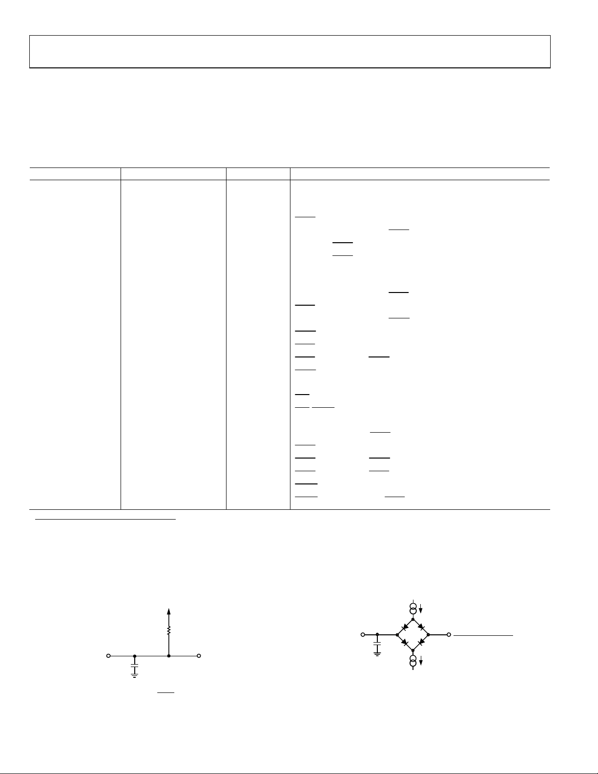
CL50pF
Figure 2. Load Circuit for
CC
R
2.2kΩ
L
BUSY
Timing Diagram
200µA
TO
OUTPUT
PIN
CL 50pF
V
OL
03165-002
200µA
Figure 3. Load Circuit for SDO Timing Diagram
(Serial Interface, Daisy- Chain Mode)
I
OL
V
(min) + VOL(max)
OH
2
I
OH
03165-003
Rev. A | Page 6 of 28
Page 7
AD5379
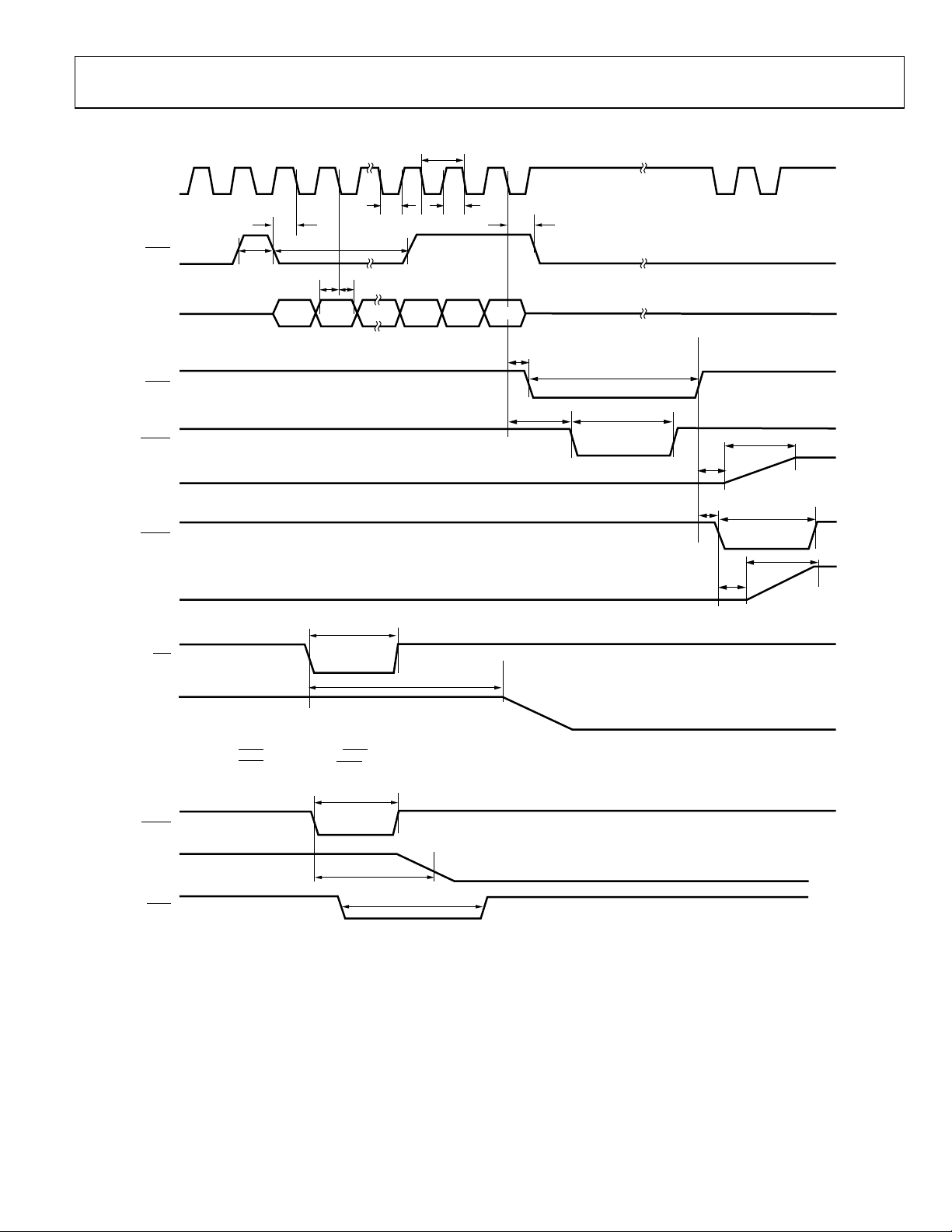
t
1
SCLK
SYNC
BUSY
LDAC
VOUT
LDAC
VOUT
DIN
1 2 24 24
t
3
t
4
t
7
DB23 DB0
1
2
t8t
t
6
9
t
18
t
2
t
5
t
10
t
12
t
11
t
13
t
17
t
14
t
15
t
13
t
t
17
16
CLR
t
19
VOUT
1
LDAC ACTIVE DURING BUSY
2
LDAC ACTIVE AFTER BUSY
t
25
RESET
VOUT
BUSY
t
19
t
26
03165-004
Figure 4. Serial Interface Timing Diagram (Standalone Mode)
Rev. A | Page 7 of 28
Page 8
AD5379
t
1
SCLK
SYNC
DIN
SDO
LDAC
BUSY
t
t
7
t
4
t8t
INPUT WORD FOR DAC N
3
9
24 48
t
2
D0 D0'D23'D23
INPUT WORD FOR DAC N+1
t
20
D23 D0
INPUT WORD FOR DAC NUNDEFINED
t
t
21
22
t13t
23
t
24
t
11
03165-005
Figure 5. Serial Interface Timing Diagram (Daisy-Chain Mode)
Rev. A | Page 8 of 28
Page 9
AD5379
PARALLEL INTERFACE
VCC = 2.7 V to 5.5 V; VDD = 11.4 V to 16.5 V; VSS = −11.4 V to −16.5 V; AGND = DGND = DUTGND = 0 V; V
(−) = −3.5 V, FIFOEN = 0 V; all specifications T
V
REF
MIN
to T
, unless otherwise noted.
MAX
(+) = 5 V;
REF
Table 5.
Parameter
t
0
t
1
t
2
t
3
t
4
t
5
t
6
t
7
t
8
t
9
4
t
10
4
t
11
t
12
t
13
t
14
4
t
15
t
16
t
17
t
18
t
19
t
20
t
21
t
22
t
23
1, , 2 3
Limit at T
4.5 ns min
4.5 ns min
10 ns min
10 ns min
0 ns min
0 ns min
4.5 ns min
4.5 ns min
20 ns min
240 ns min
0/30 ns min/max
330 ns max
0 ns min
30 ns min
20 ns min
150 ns typ
20 ns min
0 ns min
100 ns typ
MIN
to T
MAX
Unit Description
REG0, REG1, address to
REG0, REG1, address to
CS
pulse width low.
WR
pulse width low.
CS
to WR falling edge setup time.
WR
to CS rising edge hold time.
Data to WR rising edge setup time.
WR
Data to
WR
pulse width high.
Minimum
WR
rising edge to
BUSY
BUSY
WR
rising edge to
LDAC
BUSY
LDAC
BUSY
LDAC
rising edge hold time.
WR
cycle time (single-channel write).
pulse width low (single-channel update). See Table 10.
rising edge to WR rising edge.
pulse width low.
rising edge to DAC output response time.
rising edge to WR rising edge.
rising edge to
falling edge to DAC output response time.
20/30 µs typ/ max DAC output settling time.
10 ns min
350 ns max
10 ns min
120 µs max
CLR
pulse width low.
CLR/RESET
RESET
RESET
pulse activation time.
pulse width low.
time indicated by
1
Guaranteed by design and characterization, not production tested.
2
All input signals are specified with tr = tf = 2 ns (10% to 90% of VCC), and timed from a voltage level of 1.2 V.
3
See . Figure 6
4
Measured with load circuit shown in . Figure 2
WR
WR
BUSY
falling edge.
LDAC
falling edge.
LDAC
rising edge setup time.
rising edge hold time.
falling edge.
BUSY
low.
Rev. A | Page 9 of 28
Page 10

AD5379
t
t
0
REG0,
REG1,
A7–A02
CS
WR
DB12–DB0
BUSY
LDAC
VOUT
LDAC
VOUT
t
4
t
2
t
3
t
1
2
1
t
5
t
9
t
8
t
6
7
t
10
t
13
t
20
t
11
t
14
t
16
t
12
t
19
t
15
t
17
t
14
t
19
t
18
CLR
VOUT
RESET
VOUT
BUSY
1
LDAC ACTIVE DURING BUSY
2
LDAC ACTIVE AFTER BUSY
t
22
Figure 6. Parallel Interface Timing Diagram
t
21
t
21
t
23
03165-006
Rev. A | Page 10 of 28
Page 11

AD5379
ABSOLUTE MAXIMUM RATINGS
TA = 25°C, unless otherwise noted.
Transient currents of up to 100 mA do not cause SCR latch-up.
Table 6.
Parameter Rating
VDD to AGND −0.3 V to +17 V
VSS to AGND −17 V to +0.3 V
VCC to DGND −0.3 V to +7 V
Digital Inputs to DGND −0.3 V to VCC + 0.3 V
Digital Outputs to DGND −0.3 V to VCC + 0.3 V
V
1(+), V
REF
V
1(−), V
REF
V
to AGND −0.3 V to +7 V
BIAS
VOUT0–VOUT39 to AGND VSS − 0.3 V to VDD + 0.3 V
REFGND to AGND VSS − 0.3 V to VDD + 0.3 V
AGND to DGND −0.3 V to +0.3 V
Operating Temperature Range (TA)
Industrial (A Version) −40°C to +85°C
Storage Temperature Range −65°C to +150°C
Junction Temperature (TJ max) 150°C
108-Lead CSPBGA Package
θJA Thermal Impedance 37.5°C/W
θJC Thermal Impedance 8.5°C/W
Reflow Soldering
Peak Temperature 230°C
Time at Peak Temperature 10 sec to 40 sec
2(+) to AGND −0.3 V to +7 V
REF
2(−) to AGND VSS − 0.3 V to VDD + 0.3 V
REF
Stresses above those listed under Absolute Maximum Ratings
may cause permanent damage to the device. This is a stress
rating only, and functional operation of the device at these or
any other conditions above those listed in the operational
sections of this specification is not implied. Exposure to
absolute maximum rating conditions for extended periods may
affect device reliability.
ESD CAUTION
ESD (electrostatic discharge) sensitive device. Electrostatic charges as high as 4000 V readily accumulate
on the human body and test equipment and can discharge without detection. Although this product
features proprietary ESD protection circuitry, permanent damage may occur on devices subjected to
high energy electrostatic discharges. Therefore, proper ESD precautions are recommended to avoid
performance degradation or loss of functionality.
Rev. A | Page 11 of 28
Page 12

AD5379
PIN CONFIGURATION AND FUNCTION DESCRIPTIONS
123456789101112
A
B
C
D
E
F
G
H
J
K
L
M
123456789101112
AD5379
TOP VIEW
A
B
C
D
E
F
G
H
J
K
L
M
03165-007
Figure 7. Pin Configuration
Table 7. 108-Lead CSPBGA Ball Configuration
CSPBGA
Number Ball Name
A1 REG0
A2 VCC3
A3 DB10
A4 AGND4
A5 V
BIAS
A6 VOUT5
A7 AGND3
A8 REFGNDA1
A9 V
A10 V
A11 V
A12 V
5
DD
5
SS
4
SS
4
DD
B1 REG1
B2 DGND4
B3 DB9
B4
CLR
B5 VOUT7
B6 VOUT6
B7 VOUT0
B8 VOUT1
B9 VOUT2
B10 VOUT31
B11 REFGNDD1
B12 VOUT30
C1 DB13
C2 DB12/SCLK
C3 DB11/DIN
1
C4
1
An internal 1 MΩ pull-down device is located on this logic input; therefore, it can be left floating and defaults to a logic low condition.
2
An internal 1 MΩ pull-up device is located on this logic input; therefore, it can be left floating and defaults to a logic high condition.
3
N/C—Do not connect to this pin. Internal active pull-up device on these logic inputs. They default to a logic high condition.
SER/
PAR
CSPBGA
Number Ball Name
C5
LDAC
C6 VOUT8
C7 VOUT3
C8 VOUT4
C9 VOUT9
C10 VOUT34
C11 VOUT32
C12 VOUT33
D1 DB7
D2 DB8
D3 DGND1
D10 V
1(−)
REF
D11 VOUT35
D12 VOUT36
E1 DB5
E2 DB6
E3 V
1
CC
E10 REFGNDB2
E11 VOUT37
E12 VOUT38
F1 DB4
F2 DB3
F3 DB2
F10 V
3
DD
F11 REFGNDD2
F12 VOUT39
G1 DB1
CSPBGA
Number Ball Name
G3 BUSY
G10 VSS3
G11 VOUT29
G12 REFGNDC2
H1
H2 SDO
H3 CS/SYNC
H10 VOUT28
H11 VOUT26
H12 VOUT27
J1 A0
J2 A1
J3 A2
J10 VOUT19
J11 VOUT24
J12 VOUT25
K1 A4
K2 A5
K3 A3
K4 DGND2
K5 REFGNDA2
K6 V
K7 VOUT12
K8 VOUT13
K9 VOUT16
K10 VOUT18
K11 VOUT22
G2 DB0
WR
/DCEN
2(−)
REF
2
CSPBGA
Number Ball Name
K12 VOUT23
L1 A7
L2 A6
L3 N/C
L4 RESET
3
2
L5 VOUT17
L6 AGND2
L7 VOUT14
L8 VOUT10
L9 V
L10 V
1
DD
2(+)
REF
L11 VOUT20
L12 VOUT21
M1 DGND3
M2 V
M3 FIFOEN
2
CC
1
M4 AGND1
M5 VOUT15
M6 VOUT11
M7 REFGNDB1
M8 V
M9 V
M10 V
M11 V
1(+)
REF
1
SS
2
SS
2
DD
M12 REFGNDC1
Rev. A | Page 12 of 28
Page 13

AD5379
Table 8. Pin Function Descriptions
Pin Function
VCC(1–3)
VSS(1–5)
VDD(1–5)
AGND(1–4) Ground for All Analog Circuitry. All AGND pins should be connected to the AGND plane.
DGND(1–4) Ground for All Digital Circuitry. All DGND pins should be connected to the DGND plane.
V
V
V
REF
REF
BIAS
1(+), V
2(+), V
1(−) Reference Inputs for DACs 0 to 7, 10 to 17, 20 to 27, and 30 to 37. These voltages are referred to AGND.
REF
2(−) Reference Inputs for DACs 8, 9, 18, 19, 28, 29, 38, and 39. These reference voltages are referred to AGND.
REF
VOUT0 to VOUT39
SER/PAR Interface Select Input. This pin allows the user to select whether the serial or parallel interface is used. This pin has an
1
SYNC
SCLK1
DIN1 Serial Data Input. Data must be valid on the falling edge of SCLK.
SDO1
DCEN1
CS
WR
DB13 to DB0
A0 to A7
REG0
CLR
BUSY Digital Input/Open-Drain Output. This pin must be pulled high with a pull-up resistor for correct operation. BUSY goes
LDAC
Logic Power Supply; 2.7 V to 5.5 V. These pins should be decoupled with 0.1 µF ceramic capacitors and 10 µF
capacitors.
Negative Analog Power Supply; −11.4 V to −16.5 V for Specified Performance. These pins should be decoupled with
0.1 µF ceramic capacitors and 10 µF capacitors.
Positive Analog Power Supply; +11.4 V to +16.5 V for Specified Performance. These pins should be decoupled with
0.1 µF ceramic capacitors and 10 µF capacitors.
DAC Bias Voltage Input/Output. This pin provides an access to the on-chip voltage generator voltage and is provided
for bypassing and overdriving purposes only. If V
higher potential (for example, 5 V). If V
(+) < 4.25 V, the on-chip bias generator can be used. In this case, the V
REF
(+) > 4.25 V, V
REF
must be pulled high externally to an equal or
BIAS
BIAS
pin
should be decoupled with a 10 nF capacitor to AGND.
DAC Outputs. Buffered analog outputs for each of the 40 DAC channels. Each analog output is capable of driving an
output load of 5 kΩ to ground. Typical output impedance of these amplifiers is 1 Ω.
internal 1 MΩ pull-down resistor, meaning that the default state at power-on is parallel mode. If this pin is tied high,
the serial interface is used.
Active Low Input. This is the frame synchronization signal for the serial interface.
Serial Clock Input. Data is clocked into the shift register on the falling edge of SCLK. This pin operates at clock speeds
up to 50 MHz.
Serial Data Output. CMOS output. SDO can be used for daisy-chaining a number of devices together. Data is clocked
out on SDO on the rising edge of SCLK and is valid on the falling edge of SCLK.
Daisy-Chain Select Input (Level Sensitive, Active High). When high, this signal is used in conjunction with SER/
PAR
high to enable serial interface daisy-chain mode.
Parallel Interface Chip Select Input (Level Sensitive, Active Low). If this pin is low, the device is selected.
Parallel Interface Write Input (Edge Sensitive). The rising edge of WR is used in conjunction with CS low and the
address bus inputs to write to the selected AD5379 registers.
Parallel Data Inputs. The AD5379 can accept a straight 14-bit parallel word on DB0 to DB13, where DB13 is the MSB
and DB0 is the LSB.
Parallel Address Inputs. A7 to A4 are decoded to select one group or multiple groups of registers (input registers, gain
registers (m) or offset registers (c)) for a data transfer. This pin is used in conjunction with the REG1 and REG0 pins to
determine the destination register for the input data. See the Parallel Interface section for details of the address
decoding.
Parallel Interface Register Select Input. This pin is used together with REG1 to select data registers, gain registers,
offset registers, increment/decrement mode, or the soft reset function. See Table 11.
Asynchronous Clear Input (Level Sensitive, Active Low). When
stages, VOUT0 to VOUT39, is switched to the externally set potential on the relevant REFGND pin. While
LDAC
pulses are ignored. When
CLR
is taken high again, the DAC outputs remain cleared until
contents of input registers and DAC registers 0 to 39 are not affected by taking
CLR
is low, the input to each of the DAC output buffer
CLR
LDAC
is taken low. The
CLR
low.
is low, all
low during internal calculations of x2. During this time, the user can continue writing new data to additional ×1, c,
and m registers (these are stored in a FIFO), but no further updates to the DAC registers and DAC outputs can take
LDAC
place. If
externally to delay
RESET
is taken low while
LDAC action. BUSY also goes low during power-on reset or when the
operation, the parallel interface is disabled and any events on
Load DAC Logic Input (Active Low). If
registers are transferred to the DAC registers and the DAC outputs are updated. If
active and internal calculations are taking place, the
BUSY
goes inactive. However, any events on
BUSY
is low, this event is stored. Because
LDAC
is taken low while
LDAC
event is stored and the DAC registers are updated when
LDAC
during power-on reset or
BUSY
is bidirectional, it can be pulled low
RESET
pin is low. During a
LDAC
are ignored.
BUSY
is inactive (high), the contents of the input
LDAC
is taken low while
RESET
are ignored.
BUSY
is
Rev. A | Page 13 of 28
Page 14

AD5379
Pin Function
FIFOEN
RESET
REFGNDA1 Reference Ground for DACs 0 to 7. VOUT0 to VOUT7 are referenced to this voltage.
REFGNDA2 Reference Ground for DACs 8 and 9. VOUT8 and VOUT9 are referenced to this voltage.
REFGNDB1 Reference Ground for DACs 10 to 17. VOUT10 to VOUT17 are referenced to this voltage.
REFGNDB2 Reference Ground for DACs 18 and 19. VOUT18 and VOUT19 are referenced to this voltage.
REFGNDC1 Reference Ground for DACs 20 to 27. VOUT20 to VOUT27 are referenced to this voltage.
REFGNDC2 Reference Ground for DACs 28 and 29. VOUT28 and VOUT29 are referenced to this voltage.
REFGNDD1 Reference Ground for DACs 30 to 37. VOUT30 to VOUT37 are referenced to this voltage.
REFGNDD2 Reference Ground for DACs 38 and 39. VOUT38 and VOUT39 are referenced to this voltage.
1
These serial interface signals do not require separate pins, but share parallel interface pins.
FIFO Enable (Level Sensitive, Active High). When connected to DVDD, the internal FIFO is enabled, allowing the user
to write to the device at full speed. FIFO is available in both serial and parallel mode. The FIFOEN pin has an internal
1 MΩ pull-down resistor connected to ground, meaning that the FIFO is disabled by default.
Asynchronous Digital Reset Input (Falling Edge Sensitive). If unused,
RESET
up resistor (1 MΩ) ensures that the
power-on reset generator. When this pin is taken low, the AD5379 state machine initiates a reset sequence to digitally
reset x1, m, c, and x2 registers to their default power-on values. This sequence takes 100 µs (typ). Furthermore, the
input to each of the DAC output buffer stages, VOUT0 to VOUT39, is switched to the externally set potential on the
relevant REFGND pin. During
BUSY
until
goes high. When
RESET, BUSY
RESET
input is held high. The function of this pin is equivalent to that of the
goes low and the parallel interface is disabled. All
is taken high again, the DAC ouputs remain at REFGND until
RESET
may be left unconnected; an internal pull-
LDAC
pulses are ignored
LDAC
is taken low.
Rev. A | Page 14 of 28
Page 15

AD5379
TERMINOLOGY
Relative Accuracy
Relative accuracy, or endpoint linearity, is a measure of the
maximum deviation from a straight line passing through the
endpoints of the DAC transfer function. It is measured after
adjusting for zero-scale error and full-scale error and is
expressed in least significant bits (LSB).
Differential Nonlinearity
Differential nonlinearity is the difference between the measured
change and the ideal 1 LSB change between any two adjacent
codes. A specified differential nonlinearity of 1 LSB maximum
ensures monotonicity.
Zero-Scale Error
Zero-scale error is the error in the DAC output voltage when all
0s are loaded into the DAC register.
Ideally, with all 0s loaded to the DAC and m is all 1s,
c is 10 0000 0000 0000:
VOUT
= 2.5 × (VREF(−) − AGND) + REFGND
(zero scale)
Zero-scale error is a measure of the difference between VOUT
(actual) and VOUT (ideal) expressed in mV. Zero-scale error is
mainly due to offsets in the output amplifier.
Full-Scale Error
Full-scale error is the error in DAC output voltage when all 1s
are loaded into the DAC register.
Ideally, with all 1s loaded to the DAC and m is all 1s,
c is 10 0000 0000 0000:
DC Crosstalk
The 40 DAC outputs are buffered by op amps that share
common V
and VSS power supplies. If the dc load current
DD
changes in one channel (due to an update), this can result in a
further dc change in one or more channel outputs. This effect is
more significant at high load currents and reduces as the load
currents are reduced. With high impedance loads, the effect is
virtually unmeasurable. Multiple V
and VSS terminals are
DD
provided to minimize dc crosstalk.
Output Voltage Settling Time
The amount of time it takes for the output of a DAC to settle to
a specified level for a full-scale input change.
Digital-to-Analog Glitch Energy
The amount of energy injected into the analog output at the
major code transition. It is specified as the area of the glitch in
nV-s. It is measured by toggling the DAC register data between
0x1FFF and 0x2000.
Channel-to-Channel Isolation
Channel-to-channel isolation refers to the proportion of input
signal from one DAC’s reference input that appears at the
output of another DAC operating from another reference. It is
expressed in dB and measured at midscale.
DAC-to-DAC Crosstalk
DAC-to-DAC crosstalk is the glitch impulse that appears at the
output of one converter due to both the digital change and
subsequent analog output change at another converter. It is
specified in nV-s.
VOUT
= 3.5 × (VREF(+) − AGND) + 2.5 ×
(full scale)
(VREF(−)− AGND) + REFGND
Full-scale error is a measure of the difference between VOUT
(actual) and VOUT (ideal) expressed in mV. It does not include
zero-scale error.
Gain Error
Gain error is the difference between full-scale error and zeroscale error. It is expressed in mV.
Gain Error = Full-Scale Error − Zero-Scale Error
VOUT Temperature Coefficient
This includes output error contributions from linearity, offset,
and gain drift.
DC Output Impedance
DC output impedance is the effective output source resistance.
It is dominated by package lead resistance.
Rev. A | Page 15 of 28
Digital Crosstalk
The glitch impulse transferred to the output of one converter
due to a change in the DAC register code of another converter is
defined as the digital crosstalk and is specified in nV-s.
Digital Feedthrough
When the device is not selected, high frequency logic activity
on the device’s digital inputs can be capacitively coupled both
across and through the device to show up as noise on the
VOUT pins. It can also be coupled along the supply and ground
lines. This noise is digital feedthrough.
Output Noise Spectral Density
Output noise spectral density is a measure of internally
generated random noise. Random noise is characterized as a
spectral density (voltage per √Hz). It is measured by loading all
DACs to midscale and measuring noise at the output. It is
1/2
measured in nV/(Hz)
.
Page 16

AD5379
TYPICAL PERFORMANCE CHARACTERISTICS
1.5
1.0
0.5
0
INL (LSB)
–0.5
VDD = +12V
V
= –12V
SS
V
(+) = +5V
REF
V
(–) = –3.5V
REF
T
= 25°C
A
416
3
)
03165-008
03165-009
FREQUENCY
–1.0
–1.5
1400
1200
1000
800
600
400
200
VDD = +12V
V
V
V
0
3
2
1
8624010121
AD5379 CODE (10
Figure 8. Typical INL Plot
= –12V
SS
(+) = +5V
REF
(–) = –3.5V
REF
–1 0–3 –2 1 2 3
INL ERROR (LSB)
Figure 9. INL Error Distribution
(−40°C, +25°C, +85°C Superimposed)
VDD = +12V
V
= –12V
SS
V
(+) = +5V
REF
V
(–) = –3.5V
REF
T
= +85°C
MAX
3
2
1
0
–1
ERROR (mV)
–2
–3
–4
FS
TEMPERATURE (°C)
VDD = +12V
V
= –12V
SS
V
(+) = +5V
REF
V
(–) = –3.5V
REF
T
= +85°C
MAX
ZC
4020–20 0–40 60 80
Figure 11. Typical Full-Scale and Zero-Scale Errors vs. Temperature
19.0
VDD = +12V
V
= –12V
SS
10.0 10.5 11.0 11.5 12.0 12.5 13.0 13.5 14.0 14.5 15.0
(mA)
DD
I
18.9
18.8
18.7
18.6
18.5
18.4
18.3
18.2
18.1
V
REF
V
REF
+85°C
Figure 12. I
(+) = +5V
(–) = –3.5V
+25°C
V
(V)
DD
vs. VDD over Temperature
DD
–40°C
–14.6
–14.8
–15.0
–40°C
VDD = +12V
VSS = –12V
V
REF
V
REF
(+) = +5V
(–) = –3.5V
03165-011
03165-012
0
INL ERROR (LSB)
–1
–2
–3
–40 –20 0 20 40 60 80
TEMPERATURE (°C)
Figure 10. Typical INL Error vs. Temperature
(mA)
I
03165-010
Rev. A | Page 16 of 28
–15.2
SS
–15.4
–15.6
–15.8
10.0 10.5 11.0 11.5 12.0 12.5 13.0 13.5 14.0 14.5 15.0
Figure 13.I
+25°C
+85°C
V
(V)
DD
vs. VDD over Temperature
SS
03165-013
Page 17

AD5379
(mA)
CC
I
3.5
3.0
2.5
2.0
1.5
1.0
0.5
VDD = +12V
V
= –12V
SS
V
(+) = +5V
REF
V
(–) = –3.5V
REF
–40°C
+25°C
+85°C
V
OUT
TA = 25°C
V
= +12V
DD
= –12V
V
SS
(+) = +5V
V
REF
(–) = –3.5V
V
REF
0
3.5 4.02.5 3.0 4.5 5.0 5.5
FREQUENCY (MHz)
Figure 14. I
vs. Supply
CC
–0.208
–0.211
–0.214
–0.217
AMPLITUDE (V)
–0.220
–0.223
0 4 8 12 16 20
TIME (µs)
Figure 15. Major Code Transition Glitch Energy
–0.208
TA = 25°C
V
DD
= +12V
V
SS
V
REF
= –12V
(+) = +5V
V
REF
(–) = –3.5V
TA = 25°C
= +12V
V
DD
= –12V
V
SS
(+) = +5V
V
REF
(–) = –3.5V
V
REF
03165-014
03165-015
5mV10V
03165-017
Figure 17. DAC-to-DAC Crosstalk
(mA)
CC
I
1.75
1.70
1.65
1.60
1.55
1.50
1.45
1.40
1.35
1.30
1.2 1.6 2.0 2.4 2.8 3.20.4 0.80
INPUT VOLTAGE (V)
TA = 25°C
V
= +12V
DD
V
= –12V
SS
V
(+) = +5V
REF
V
(–) = –3.5V
REF
V
= +3.3V
CC
03165-018
Figure 18. Supply Current vs. Digital Input Voltage
–0.209
AMPLITUDE (V)
–0.210
–0.211
0 1.4 2.8 4.2 5.6 6.0
TIME (µs)
Figure 16. Digital Feedthrough
03165-016
Rev. A | Page 17 of 28
Page 18

AD5379
FUNCTIONAL DESCRIPTION
DAC ARCHITECTURE—GENERAL
The AD5379 contains 40 DAC channels and 40 output
amplifiers in a single package. The architecture of a single DAC
channel consists of a 14-bit resistor-string DAC followed by an
output buffer amplifier. The resistor-string section is simply a
string of resistors, each of value R, from V
type of architecture guarantees DAC monotonicity. The 14-bit
binary digital code loaded to the DAC register determines at
which node on the string the voltage is tapped off before being
fed into the output amplifier. The output amplifier translates the
output of the DAC to a wider range. The DAC output is gained
up by a factor of 3.5 and offset by the voltage on the V
See the Transfer Function section for more information.
CHANNEL GROUPS
The 40 DAC channels on the AD5379 are arranged into four
groups (A, B, C, D) of 10 channels. In each group, eight
channels are connected to V
1(+) and V
REF
remaining two channels are connected to V
2(−). Each group has two individual REFGND pins. For
V
REF
example, in Group A, eight channels are connected to
REFGNDA1, and the remaining two channels are connected to
REFGNDA2. In addition to an input register (x1) and a DAC
register (x2), each channel has a gain register (m) and an offset
register (c). See Table 17. The inclusion of these registers allows
the user to calibrate out errors in the complete signal chain,
including the DAC errors.
Table 9 shows the reference and REFGND inputs, and the
m and c registers for Group A. Groups B, C, and D are similar.
Table 9. Inputs and Registers for Group A
Channel Reference REFGND m, c Registers
0 to 7 V
8 and 9 V
REF
REF
1(+), V
2(+), V
1(−) REFGNDA1 m REG0 to REG7
REF
2(−) REFGNDA2 m REG8 and REG9
REF
TRANSFER FUNCTION
The digital input transfer function for each DAC can be
represented as
13
x2 = [(m + 1)/2
× x1] + (c − 2
where:
x2 is the data-word loaded to the resistor string DAC.
(Default is 10 0000 0000 0000.)
x1 is the 14-bit data-word written to the DAC input register.
(Default is 10 0000 0000 0000.)
m is the 13-bit gain coefficient. (Default is 1 1111 1111 1111.)
c is the 14-bit offset coefficient. (Default is 10 0000 0000 0000.)
n is the DAC resolution (n = 14).
n−1
(+) to AGND. This
REF
1(−), and the
REF
2(+) and
REF
c REG0 to REG7
c REG8 and REG9
)
(−) pin.
REF
Figure 19 shows a single DAC channel and its associated
registers. The power-on values for the m and c registers are full
scale and 0x2000, respectively. The user can individually adjust
the voltage range on each DAC channel by overwriting the
power-on values of m and c. The AD5379 has digital overflow
and underflow detection circuitry to clamp the DAC output at
full scale or zero scale when the values chosen for x1, m, and c
result in x2 being out of range.
V
INPUT
DATA
DAC
x1 INPUT
REG
x2
m REG
c REG
REG
Figure 19. Single DAC Channel
LDAC
DAC
REG
DACx2
AGND
REF
(+)
VDAC
The complete transfer function for the AD5379 can be
represented as
14
VOUT = 3.5 × ((VREF(+)− AGND) × x2/2
) +
2.5 × (VREF(−)− AGND) + REFGND
where:
x2 is the data word loaded to the resistor string DAC.
(+) is the voltage at the positive reference pin.
V
REF
V
(−) is the voltage at the negative reference pin.
REF
Figure 20 shows the output amplifier stage of a single channel.
VDAC is the voltage output from the resistor string DAC. The
nominal range of VDAC is 1 LSB to full scale.
(–)
V
REF
REFGND
R
2.5R
AGND
Figure 20. Output Amplifier Stage
R
VDAC
2.5R
R
VOUT
03165-019
03165-020
Rev. A | Page 18 of 28
Page 19

AD5379
V
FUNCTION
BIAS
The AD5379 has an on-chip voltage generator that provides a
bias voltage of 4.25 V (minimum). The V
pin is provided for
BIAS
bypassing and overdriving purposes only. It is not intended to
be used as a supply or a reference. If V
(+) > 4.25 V, V
REF
BIAS
must
be pulled high externally to an equal or higher potential (such
as 5 V). The external voltage source should be capable of
driving a 50 µA (typical) current sink load.
REFERENCE SELECTION
The voltages applied to V
output voltage range and span on VOUT0 to VOUT39. If the
offset and gain features are not used (m and c are left at their
power-on values), the required reference levels can be
calculated as follows:
VREF(+)
VREF(−)
= (VOUT
min
= (AGND + VOUT
max
If the offset and gain features of the AD5379 are used, then the
required output range is slightly different. The chosen output
range should take into account the offset and gain errors that
need to be trimmed out. Therefore, the chosen output range
should be larger than the actual, required range.
The required reference levels can be calculated as follows:
1. Identify the nominal output range on VOUT.
(+) and V
REF
− VOUT
max
(−) determine the
REF
)/3.5
min
)/2.5
min
If this offset error is too large to calibrate, then adjust the
negative reference value to account for this using the following
equation:
V
(−)
= V
REF
NEW
(−)A − V
REF
OFFSET
/2.625
Reference Selection Example
Nominal Output Range = 10 V; (−2 V to +8 V)
Offset Error = ±100 mV;
Gain Error = ±3%;
REFGND = AGND = 0 V;
1) Gain Error = ±3%;
=> Maximum Positive Gain Error = +3%
=> Output Range incl. Gain Error = 10 + 0.03(10) = 10.3 V
2) Offset Error = ±100 mV;
=> Maximum Offset Error Span = 2(100) mV = 0.2 V
=> Output Range including Gain Error and
Offset Error = 10.3 + 0.2 = 10.5 V
3) V
(+) and V
REF
(−) Calculation:
REF
Actual Output Range = 10.5 V, that is, −2.25 V to +8.25 V
(centered);
(+) = (8.25 + 2.25)/3.5 = 3 V
=> V
REF
(−) = −2.25/+2.5 = −0.9 V
V
REF
If the solution yields inconvenient reference levels, the user can
adopt one of three approaches:
2. Identify the maximum offset span and the maximum gain
required on the full output signal range.
3. Calculate the new maximum output range on VOUT
including the expected, maximum offset and gain errors.
4. Choose the new required VOUT
and VOUT
max
, keeping
min
the new VOUT limits centered on the nominal values and
assuming REFGND is zero (or equal to AGND). Note that
and VSS must provide sufficient headroom.
V
DD
5. Calculate the values of V
V
(+)
REF
V
REF
= (VOUT
min
(−)
= (AGND + VOUT
max
− VOUT
max
(+) and V
REF
min
min
)/2.5
(−) as follows:
REF
)/3.5
In addition, when using reference values other than those
suggested (V
(+) = 5 V and V
REF
(−) = −3.5 V), the expected
REF
offset error component changes to
V
OFFSET
= 0.125 × (V
(−)A + 0.7 × V
REF
REF
(+)A)
where:
(−)A is the new negative reference value.
V
REF
(+)A is the new positive reference value.
V
REF
• Use a resistor divider to divide down a convenient, higher
reference level to the required level.
(+)
• Select convenient reference levels above V
V
(−)
REF
. Modify the gain and offset registers to digitally
max
REF
or below
min
downsize the references. In this way, the user can use
almost any convenient reference level, but may reduce
performance by overcompaction of the transfer function.
• Use a combination of these two approaches.
Rev. A | Page 19 of 28
Page 20

AD5379
CALIBRATION
The user can perform a system calibration by overwriting the
default values in the m and c registers for any individual DAC
channel as follows:
• Calculate the nominal offset and gain coefficients for the
new output range (see previous example).
• Calculate the new m and c values for each channel based
on the specified offset and gain errors.
Calibration Example
Nominal Offset Coefficient = 0
Nominal Gain Coefficient =
10/10.5 × 8191 = 0.95238 × 8191 = 7801
Example 1: Channel 0, Gain Error = 3%, Offset Error = 100 mV
1) Gain Error (3%) Calibration: 7801 × 1.03 = 8035
=> Load Code “1 1111 0110 0011” to m Register 0
2) Offset Error (100 mV) Calibration:
LSB Size = 10.5/16384 = 641 µV;
Offset Coefficient for 100 mV Offset = 100/0.64 = 156 LSBs
=> Load “10 0000 1001 1100” to c Register 0
Example 2: Channel 1, Gain Error = −3%, Offset Error = −100 mV
1) Gain Error (−3%) Calibration: 7801 × 0.97 = 7567
=> Load Code “1 1110 1000 1111” to m Register 1
2) Offset Error (−100 mV) Calibration:
LSB Size = 10.5/16384 = 641 µV;
Offset Coefficient for −100 mV Offset = −100/0.64 = −156 LSBs
=> Load “01 1111 0110 0100” to c Register 1
CLEAR FUNCTION
The clear function on the AD5379 can be implemented in
hardware or software.
Hardware Clear
Bringing the
VOUT39, to the externally set potential on the REFGND pin.
This is achieved by switching in REFGND and reconfiguring
the output amplifier stages into unity gain buffer mode, thus
ensuring VOUT = REFGND. The contents of the input registers
and DAC registers are not affected by taking
CLR
is brought high, the DAC outputs remain cleared until
LDAC
ignored.
CLR
pin low switches the outputs, VOUT0 to
is taken low. While
CLR
is low, the value of
CLR
low. When
LDAC
is
Software Clear
Loading a clear code to the x1 registers also enables the user to
set VOUT0 to VOUT39 to the REFGND level. The default clear
code corresponds to m at full-scale and c at midscale (x2 = x1).
Default Clear Code
14
× (−Output Offset)/(Output Range)
= 2
14
= 2
× 2.5 × (AGND − V
(−))/(3.5 × (V
REF
(+)− AGND))
REF
The more general expression for the clear code is as follows:
14
Clear Code = (2
)/(m + 1) × (Default Clear Code − c)
BUSY AND LDAC FUNCTIONS
The value of x2 is calculated each time the user writes new data
to the corresponding x1, c, or m registers. During the calculation of x2, the
BUSY
output goes low. While
user can continue writing new data to the x1, m, or c registers,
but no DAC output updates can take place. The DAC outputs
are updated by taking the
BUSY
while
is active, the
outputs update immediately after
also hold the
LDAC
LDAC
input low. If
LDAC
event is stored and the DAC
BUSY
input permanently low. In this case, the
DAC outputs update immediately after
Table 10.
Action
Loading x1, c, or m to 1 channel 530 330
Loading x1, c, or m to 2 channels 700 500
Loading x1, c, or m to 3 channels 900 700
Loading x1, c, or m to 4 channels 1050 850
Loading x1, c, or m to all
40 channels
BUSY
Pulse Width
BUSY
FIFO
Enabled
5500 5300
The value of x2 for a single channel or group of channels is
recalculated each time there is a write to any x1 register(s),
c register(s), or m register(s). During the calculation of x2,
BUSY
goes low. The duration of this
the number of channels being updated. For example, if x1, c, or
m data is written to one DAC channel,
550 ns (maximum). However, if data is written to two DAC
channels,
BUSY
goes low for 700 ns (maximum). As shown in
Table 10, there are approximately 200 ns of overhead due to
FIFO access.
BUSY
is low, the
LDAC
goes low
goes high. A user can
BUSY
goes high.
Pulse Width (ns max)
FIFO
Disabled
BUSY
pulse depends on
BUSY
goes low for
The AD5379 contains an extra feature whereby a DAC register
is not updated unless its x2 register has been written to since the
last time
brought low, the DAC registers are filled with the contents of
the x2 registers. However the AD5379 updates the DAC register
only if the x2 data has changed, thereby removing unnecessary
digital crosstalk.
Rev. A | Page 20 of 28
LDAC
was brought low. Normally, when
LDAC
is
Page 21

AD5379
FIFO VS. NON-FIFO OPERATION
Two modes of operation are available for loading data to the
AD5379 registers: operation with FIFO disabled and operation
with FIFO enabled. Operation with FIFO disabled is optimum
for single writes to the device. If the system requires significant
data transfers to the AD5379, however, then operation with
FIFO enabled is more efficient.
externally set potential on the REFGND pin. During power-on,
the parallel interface is disabled, so it is not possible to write to
the part. Any transitions on
are ignored in order to reject initial
rising edge on
BUSY
LDAC
during the power-on period
LDAC
pin glitching. A
indicates that power-on is complete and
that the parallel interface is enabled. All DACs remain in their
LDAC
power-on state until
is used to update the DAC outputs.
When FIFO is enabled, the AD5379 uses an internal FIFO
memory to allow high speed successive writes in both serial and
parallel modes. This optimizes the interface speed and efficiency,
minimizes the total conversion time due to internal digital
efficiencies, and minimizes the overhead on the master con-
BUSY
troller when managing the data transfers. The
signal goes
low while instructions in the state machine are being executed.
Table 10 compares operation with FIFO enabled and FIFO
disabled for different data transfers to the AD5379. Operation
with FIFO enabled is more efficient for all operations except
single write operations. When using the FIFO, the user can
continue writing new data to the AD5379 while write instructions are being executed. Up to 128 successive instructions can
be written to the FIFO at maximum speed. When the FIFO is
full, additional writes to the AD5379 are ignored.
BUSY INPUT FUNCTION
If required, because the
1
, a second AD5379 (or other device, such as a system
drain
controller), can pull
means of delaying any
synchronous updates of multiple AD5379 devices in a system, at
maximum speed. As soon as the last device connected to the
BUSY
pin is ready, all DACs update automatically. Tying the
BUSY
pin of multiple devices together enables synchronous
updating of all DACs without extra hardware.
BUSY
pin is bidirectional and open-
BUSY
low to delay DAC update(s). This is a
LDAC
action. This feature allows
POWER-ON RESET FUNCTION
The AD5379 contains a power-on reset generator and state
CLR
machine. During power-on,
the power-on state machine resets all internal registers to their
default values, and
BUSY
(typical). The outputs, VOUT0 to VOUT39, are switched to the
becomes active (internally),
goes low. This sequence takes 8 ms
RESET INPUT FUNCTION
The AD5379 can be placed in its power-on reset state at any
RESET
time by activating the
pin. The AD5379 state machine
initiates a reset sequence to digitally reset the x1, m, c, and x2
registers to their default power-on values. This sequence takes
95 µs (typical), 120 µs (maximum), 70 µs (minimum). During
this sequence,
transitions on
RESET
BUSY
goes low. While
LDAC
are ignored. As with the
is low, the DAC outputs are switched to REFGND. The
outputs remain at REFGND until an
RESET
is low, any
LDAC
pulse is applied.
CLR
input, while
This reset function can also be implemented via the parallel
interface by setting the REG0 and REG1 pins low and writing
all 1s to DB13 to DB0 (see Table 16 for soft reset).
INCREMENT/DECREMENT FUNCTION
The AD5379 has a special function register that enables the user
to increment or decrement the internal 14-bit input register
data (x1) in steps of 0 to 127 LSBs. The increment/decrement
function is selected by setting both REG1 and REG0 pins (or
bits) low. Address Pins (or Bits) A7 to A0 are used to select a
DAC channel or group of channels. The amount by which the
x1 register is incremented or decremented is determined by the
DB6 to DB0 bits/pins. For example, for a 1 LSB increment or
decrement, DB6 to DB0 = 0000001, while for a 7 LSB increment
or decrement, DB6 to DB0 = 0000111. DB8 determines whether
the input register data is incremented (DB8 = 1) or decremented (DB8 = 0). The maximum amount by which the user is
allowed to increment or decrement the data is 127 LSBs, that is,
DB6 to DB0 = 1111111. The 0 LSB step is included to facilitate
software loops in the user’s application. See Table 15.
The AD5379 has digital overflow and underflow detection
circuitry to clamp at full scale or zero scale when the values
chosen for increment or decrement mode are out of range.
1
For correct operation, use pull-up resistor to digital supply.
Rev. A | Page 21 of 28
Page 22

AD5379
INTERFACES
The AD5379 contains a serial and a parallel interface. The
PA R
active interface is selected via the SER/
The AD5379 uses an internal FIFO memory to allow high
speed successive writes in both serial and parallel modes. The
user can continue writing new data to the AD5379 while write
instructions are being executed. The
instructions in the FIFO are being executed. Up to 120 successive
instructions can be written to the FIFO at maximum speed.
When the FIFO is full, additional writes to the AD5379 are
ignored.
To minimize both the power consumption of the device and
on-chip digital noise, the active interface powers up fully only
when the device is being written to, that is, on the falling edge
WR
or on the falling edge of
of
SYNC
All digital interfaces are 2.5 V LVTTL-compatible when
operating from a 2.7 V to 3.6 V V
CC
PARALLEL INTERFACE
A pull-down on the SER/
the default. If using the parallel interface, the SER/
be left unconnected. Figure 6 shows the timing diagram for a
parallel write to the AD5379. The parallel interface is controlled
by the following pins.
CS
Pin
Active low device select pin.
WR
Pin
On the rising edge of WR, with CS low, the address values at
Pin A7 to Pin A0 are latched, and data values at Pin DB13 to
Pin DB0 are loaded into the selected AD5379 input registers.
REG1, REG0 Pins
The REG1 and REG0 pins determine the destination register of
the data being written to the AD5379. See Table 11.
Table 11. Register Selection
REG1 REG0 Register Selected
1 1 Input data register (x1)
1 0 Offset register (c)
0 1 Gain register (m)
0 0 Special function register
DB13 to DB0 Pins
The AD5379 accepts a straight, 14-bit parallel word on Pin DB0
to Pin DB13, where Pin DB13 is the MSB and Pin DB0 is the
LSB. See Table 12, Table 13, Table 14, Table 15, and Table 16.
PA R
pin makes the parallel interface
pin.
BUSY
signal goes low while
.
supply.
PA R
pin can
A7 to A0 Pins
Each of the 40 DAC channels can be individually addressed. In
addition, several channel groupings enable the user to simultaneously write the same data to multiple DAC channels. Address
Bits A7 to A4 are decoded to select one group or multiple
groups of registers. Address Bits A3 to A0 select one of ten
input data registers (x1), offset registers (c), or gain registers
(m). See Table 17.
SERIAL INTERFACE
The SER/
face and disable the parallel interface. The serial interface is
controlled by five pins, as follows.
SYNC
Standard 3-wire interface pins.
DCEN
Selects standalone mode or daisy-chain mode.
SDO
Data out pin for daisy-chain mode.
Figure 4 and Figure 5 show the timing diagrams for a serial
write to the AD5379 in standalone and daisy-chain modes,
respectively.
The 24-bit data word format for the serial interface is shown in
Figure 21.
MSB
GROUP/CHANNEL
SELECT BITS
Standalone Mode
By connecting the DCEN (daisy-chain enable) pin low,
standalone mode is enabled. The serial interface works with
both a continuous and a burst serial clock. The first falling edge
of
the number of serial clocks to ensure that the correct number of
bits is shifted into the serial shift register. Additional edges on
SYNC
Once 24 bits are shifted into the serial shift register, the SCLK is
ignored. In order for another serial transfer to take place, the
counter must be reset by the falling edge of
PA R
pin must be tied high to enable the serial inter-
, DIN, SCLK
A7–A0 REG1
REGISTER SELECT
BITS
SYNC
starts the write cycle and resets a counter that counts
REG0 DB13–DB0
REGISTER DATA BITS
Figure 21. Serial Data Format
are ignored until 24 bits are shifted into the register.
SYNC
.
LSB
03165-021
Rev. A | Page 22 of 28
Page 23

AD5379
Daisy-Chain Mode
For systems that contain several DACs, the SDO pin can be
used to daisy-chain several devices together. This daisy-chain
mode can be useful in system diagnostics and in reducing the
number of serial interface lines.
Connecting the DCEN (daisy-chain enable) pin high enables
SYNC
daisy-chain mode. The first falling edge of
write cycle. The SCLK is continuously applied to the input shift
SYNC
register when
applied, the data ripples out of the shift register and appears on
the SDO line. This data is clocked out on the rising edge of
SCLK and is valid on the falling edge. By connecting this line to
the DIN input on the next device in the chain, a multidevice
interface is constructed. For each AD5379 in the system,
24 clock pulses are required. Therefore, the total number of
is low. If more than 24 clock pulses are
starts the
clock cycles must equal 24N, where N is the total number of
AD5379 devices in the chain. If fewer than 24 clocks are
applied, the write sequence is ignored.
When the serial transfer to all devices has been completed,
SYNC
is taken high. This latches the input data in each device
in the daisy chain and prevents any additional data from being
clocked into the input shift register.
SYNC
A continuous SCLK source can be used if
the correct number of clock cycles. Alternatively, a burst clock
containing the exact number of clock cycles can be used and
SYNC
taken high after the final clock to latch the data.
When the transfer to all input registers is complete, a common
LDAC
signal updates all DAC registers, and all analog outputs
are simultaneously updated.
is held low for
Rev. A | Page 23 of 28
Page 24

AD5379
DATA DECODING
The AD5379 contains a 14-bit data bus, DB13 to DB0. Depending on the values of REG1 and REG0, this data is loaded into
the addressed DAC input register(s), offset (c) register(s), gain
(m) register(s), or the special function register.
Table 12. DAC Data Format (REG1 = 1, REG0 = 1)
DB13 to DB0 DAC Output
11 1111 1111 1111 (16383/16384) V
11 1111 1111 1110 (16382/16384) V
10 0000 0000 0001 (8193/16384) V
10 0000 0000 0000 (8192/16384) V
01 1111 1111 1111 (8191/16384) V
00 0000 0000 0001 (1/16384) V
00 0000 0000 0000 0 V
Table 13. Offset Data Format (REG1 = 1, REG0 = 0)
DB13 to DB0 Offset (LSB)
11 1111 1111 1111 +8191
11 1111 1111 1110 +8190
10 0000 0000 0001 +1
10 0000 0000 0000 +0
01 1111 1111 1111 −1
00 0000 0000 0001 −8191
00 0000 0000 0000 −8192
REF
REF
REF
REF
REF
REF
(+) V
(+) V
(+) V
(+) V
(+) V
(+) V
Table 14. Gain Data Format (REG1 = 0, REG0 = 1)
DB12 to DB1 Gain
1 1111 1111 1111 8192/8192
1 1111 1111 1110 8191/8192
1 0000 0000 0001 4098/8192
1 0000 0000 0000 4097/8192
0 1111 1111 1111 4096/8192
0 0000 0000 0001 2/8192
0 0000 0000 0000 1/8192
Table 15. Special Function Data Format (REG1 = 0, REG0 = 0)
DB13 to DB0 Increment/Decrement Step (LSB)
00000 10 1111111 +127
00000 10 0000111 +7
00000 10 0000001 +1
00000 X0 0000000 0
00000 00 0000001 −1
00000 00 0000111 −7
00000 00 1111111 −128
Table 16. Soft Reset (REG1 = 0, REG0 = 0)
DB13 to DB0 DAC Output
11 1111 1111 1111 REFGND
Rev. A | Page 24 of 28
Page 25

AD5379
ADDRESS DECODING
The AD5379 contains an 8-bit address bus, A7 to A0. This
address bus allows each DAC input register (x1), each offset (c)
register, and each gain (m) register to be individually updated.
Table 17. DAC Group Addressing
A7 A6 A5 A4 Group A3 A2 A1 A0 Data/Offset/Gain/INC-DEC Register
0 0 0 0 All 40 DACs 0 0 0 0 Register 0
0 0 0 1 Group A 0 0 0 1 Register 1
0 0 1 0 Group B 0 0 1 0 Register 2
0 0 1 1 Groups A, B 0 0 1 1 Register 3
0 1 0 0 Group C 0 1 0 0 Register 4
0 1 0 1 Groups A, C 0 1 0 1 Register 5
0 1 1 0 Groups B, C 0 1 1 0 Register 6
0 1 1 1 Groups A, B, C 0 1 1 1 Register 7
1 0 0 0 Group D 1 0 0 0 Register 8
1 0 0 1 Groups A, D 1 0 0 1 Register 9
1 0 1 0 Groups B, D
1 0 1 1 Groups A, B, D
1 1 0 0 Groups C, D
1 1 0 1 Groups A, C, D
1 1 1 0 Groups B, C, D
1 1 1 1 Groups A, B, C, D
The REG1 and REG0 bits in the special function register (SFR)
(see Table 9) show the decoding for data, offset, and gain
registers. Note that when all 40 DAC channels are selected,
Address Bit A3 to Address Bit A0 are ignored.
Rev. A | Page 25 of 28
Page 26

AD5379
POWER SUPPLY DECOUPLING
In any circuit where accuracy is important, careful consideration of the power supply and ground return layout helps to
ensure the rated performance. The printed circuit board on
which the AD5379 is mounted should be designed so that the
analog and digital sections are separated and confined to
certain areas of the board. If the AD5379 is in a system where
multiple devices require an AGND-to-DGND connection, the
connection should be made at one point only. The star ground
point should be established as close as possible to the device.
For supplies with multiple pins (V
mended to tie these pins together and to decouple each
supply once.
The AD5379 should have ample supply decoupling of 10 µF in
parallel with 0.1 µF on each supply located as close to the
package as possible, ideally right up against the device. The
10 µF capacitors are the tantalum bead type. The 0.1 µF capacitor should have low effective series resistance (ESR) and
effective series inductance (ESI), such as the common ceramic
types that provide a low impedance path to ground at high
frequencies, to handle transient currents due to internal
logic switching.
Digital lines running under the device should be avoided,
because these couple noise onto the device. The analog ground
plane should be allowed to run under the AD5379 to avoid
noise coupling. The power supply lines of the AD5379 should
use as large a trace as possible to provide low impedance paths
, VDD, VCC), it is recom-
SS
and reduce the effects of glitches on the power supply line. Fast
switching digital signals should be shielded with digital ground
to avoid radiating noise to other parts of the board, and should
never be run near the reference inputs. It is essential to minimize noise on all V
(+) and V
REF
(−) lines. The V
REF
pin should
BIAS
be decoupled with a 10 nF capacitor to AGND.
Avoid crossover of digital and analog signals. Traces on
opposite sides of the board should run at right angles to each
other. This reduces the effects of feedthrough through the
board. A microstrip technique is by far the best, but not always
possible with a double-sided board. In this technique, the
component side of the board is dedicated to ground plane,
while signal traces are placed on the solder side.
As is the case for all thin packages, care must be taken to avoid
flexing the CSPBGA package and to avoid a point load on the
surface of this package during the assembly process.
POWER-ON
An on-chip power supply monitor makes the AD5379 robust to
power sequencing. The supply monitor powers up the analog
section after (V
output buffers power-up in
potential, even if V
analog circuitry powers up, and the buffered DAC output level
settles linearly within the supply range.
− VSS) is greater than 7 V (typical). The
DD
CLR
mode forced to the DUTGND
remains at 0 V. After VSS is applied, the
CC
Rev. A | Page 26 of 28
Page 27

AD5379
TYPICAL APPLICATION CIRCUIT
The high channel count of the AD5379 makes it well-suited to
applications requiring high levels of integration such as optical
and automatic test equipment (ATE) systems. Figure 22 shows
the AD5379 as it would be used in an ATE system. Shown here
is one pin of a typical logic tester. It is apparent that a number of
discrete levels are required for the pin driver, active load circuit,
parametric measurement unit, comparators, and clamps.
GUARD AMP
DAC
V
TERM
V
H
DRIVER
V
L
DAC
ACTIVE LOAD
DRIVEN SHIELD
V
CH
V
CL
V
TH
V
TL
DAC
ADC
TIMING DATA
MEMORY
TIMING
GENERATOR
DLL LOGIC
COMPARE
MEMORY
CENTRAL PMU
DAC
DAC
FORMATTER DE-SKEW
DAC
DAC
FORMATTER DE-SKEW
DAC
DAC
DAC
DAC
COMP
I
OL
V
COM
I
OH
Figure 22. Typical Application Circuit for Logic Tester
In addition to the DAC levels required in the ATE system as
shown in Figure 22, drivers, loads, comparators, and parametric
measurement unit functions are also required. Analog Devices
provides solutions for all these functions.
DAC
PPMU
ADC
RELAYS
50
GND SENSE
Ω
COAX
DAC
ADC
DUT
DEVICE POWER
SUPPLY
03165-022
Rev. A | Page 27 of 28
Page 28

AD5379
OUTLINE DIMENSIONS
*1.85
1.70
1.55
13.00
BSC SQ
BALL A1
INDICATOR
TOP VIEW
DETAIL A
11.00
0.75
0.70
0.65
BSC
10 9 8 7 6 5 4 3 2 1
12 11
BOTTOM
DETAIL A
0.64 TYP
BALL DIAMETER
A1 CORNER
INDEX AREA
VIEW
1.00 BSC
SEATING
PLANE
A
B
C
D
E
F
G
H
J
K
L
M
1.05
1.00
0.90
0.12 MAX
COPLANARITY
*COMPLIANT WITH JEDEC STANDARDS MO-192-AAD-1
EXCEPT FOR PACKAGE HEIGHT (DIMENSION A).
Figure 23. 108-Lead Chip Scale Ball Grid Array [CSPBGA]
(BC-108-2)
Dimensions shown in millimeters
ORDERING GUIDE
Model Temperature Range Linearity Error (LSBs) Package Description Package Option
AD5379ABC −40°C to +85°C ±3 108-Lead CSPBGA BC-108-2
EVAL-AD5379EB Evaluation Board and Software
© 2005 Analog Devices, Inc. All rights reserved. Trademarks and
registered trademarks are the property of their respective owners.
D03165–0–1/05(A)
Rev. A | Page 28 of 28
 Loading...