

Page 1
Quad Ultrahigh-Speed Pin Driver
20⍀
ROUT
AD53513
GND
GND
GND
GND
GND
TVCC
THERM
1.0A/K
39nF
39nF
30⍀
50⍀
VCC1
VCC2
VCC3
VCC4
VEE1
VEE2
VEE3
VEE4
VCC
VEE
VH2
DATA2
DATAB2
INH2
INHB2
VL2
VT2
VBB
RLD2
RLD3
VBB
VH3
DATA3
DATAB3
INH3
INHB3
VL3
VT3
VH4
DATA4
DATAB4
INH4
INHB4
VL4
VT4
VBB
RLD4
RLD1
VBB
VH1
DATA1
DATAB1
INH1
INHB1
VL1
VT1
DRIVER 1
VHDCPL1
VOUT1
VLDCPL1
20⍀
ROUT
39nF
39nF
30⍀
50⍀
VHDCPL2
VOUT2
VLDCPL2
DRIVER 2
20⍀
ROUT
39nF
39nF
30⍀
50⍀
VHDCPL3
VOUT3
VLDCPL3
20⍀
ROUT
39nF
39nF
30⍀
50⍀
VHDCPL4
VOUT4
VLDCPL4
DRIVER 4
DRIVER 3
a
FEATURES
500 MHz Driver Operation (1 Gb/s)
Driver Inhibit Function
100 ps Edge Matching
Guaranteed Industry Specifications
20 ⍀ Output Impedance
5 V/ns Slew Rate
Variable Output Voltages for ECL, TTL, and CMOS
High-Speed Differential Inputs for Maximum Flexibility
Ultrasmall 100-Lead LQFP Package with Built-In
Heat Sink
APPLICATIONS
Automatic Test Equipment
Semiconductor Test Systems
Board Test Systems
Instrumentation and Characterization Equipment
PRODUCT DESCRIPTION
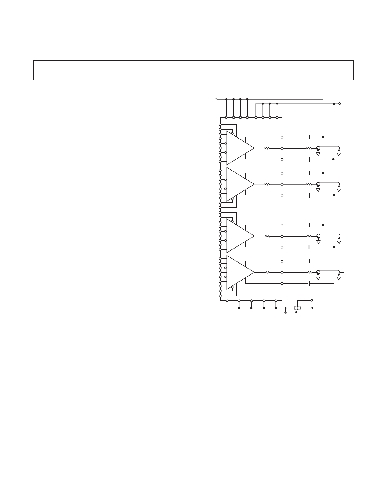
The AD53513 is a quad high-speed pin driver designed for use
in digital or mixed-signal test systems. Combining a high-speed
monolithic process with a convenient surface-mount package,
this product attains superb electrical performance while preserving
optimum packaging densities and long-term reliability in a
100-lead, LQFP package with built-in heat sink.
Featuring unity gain programmable output levels of –2.5 V to
+5.5 V, with output swing capability of less than 200 mV to
8 V, the AD53513 is designed to stimulate ECL, TTL, and
CMOS logic families, as well as high-speed memory. The
1.0 Gb/s data rate capacity and matched output impedance
allow for real-time stimulation of these digital logic families.
To test I/O devices, the pin driver can be switched into a high
impedance state (Inhibit Mode), electrically removing the driver
from the path. The pin driver leakage current in inhibit is typically
100 nA and output charge transfer entering inhibit is typically less
than 20 pC.
The AD53513 transition from HI/LO or to inhibit is controlled
through the data and inhibit inputs. The input circuitry uses
high-speed differential inputs with a common-mode range of
± 2 V. This allows for direct interface to precision differential
ECL timing. The analog logic HI/LO inputs are equally easy
to interface. Typically requiring 10 µA of bias current, the
AD53513 can be directly coupled to the output of a digitalto-analog converter.
Each channel of the AD53513 has a Mode Select Pin RLD,
which is a single-sided logic input. The logic threshold is set by
REV. 0
Information furnished by Analog Devices is believed to be accurate and
reliable. However, no responsibility is assumed by Analog Devices for its
use, nor for any infringements of patents or other rights of third parties that
may result from its use. No license is granted by implication or otherwise
under any patent or patent rights of Analog Devices.
with High-Z and V
TERM
Modes
AD53513
FUNCTIONAL BLOCK DIAGRAM
the VBB input which is common to all four channels. The RLD
Mode Select controls whether inhibit puts the driver in High-Z
or V
(DATA, DATAB, INH, INHB, RLD, VBB), must share a
common set of logic levels. The VBB threshold should be set to
the midrange of the logic levels. For example, if ECL levels of
–0.8 V to –1.8 V are used, VBB should be set to –1.3 V.
The AD53513 is available in a 100-lead, LQFP package with a
built-in heat sink and is specified to operate over the ambient
commercial temperature range of –25°C to +85°C.
One Technology Way, P.O. Box 9106, Norwood, MA 02062-9106, U.S.A.
Tel: 781/329-4700 www.analog.com
Fax: 781/326-8703 © Analog Devices, Inc., 2002
mode. (Refer to Table I.) All of the digital logic inputs
TERM
Page 2

AD53513–SPECIFICATIONS
(All specifications are at TJ = 85ⴗC ⴞ 5ⴗC, +VS = +9 V ⴞ 3%, –VS = –6 V ⴞ 3% unless otherwise noted. All temperature coefficients are measured
at TJ = 75ⴗC–95ⴗC). (A 39 nF capacitor must be connected between VCC and V
Parameter Min Typ* Max Unit Test Conditions
DIFFERENTIAL INPUT CHARACTERISTICS
(Data to DATA, INH to INH), RLD, VBB VBB = –1.3 V
Input Voltage –2 0 Volts
Differential Input Range ECL
Bias Current –1 +1 mA V
VBB Threshold Input Midrange V Set to Midrange of Logic Levels
REFERENCE INPUTS (V
, VH, VT)
L
Bias Currents –50 +50 µAV
OUTPUT CHARACTERISTICS
Logic High Range –2.3 +5.5 Volts DATA = H
Logic Low Range –2.5 +5.3 Volts DATA = L
Amplitude (V
) 0.2 8.0 Volts
H–VL
Absolute Accuracy
Offset –100 +100 mV DATA = H, VH = 0 V, VL = –2 V, VT = +3 V
V
H
V
Gain and Linearity Error ± 0.3 ± 5% of V
H
V
Offset –100 +100 mV DATA = L, VL = 0 V, VH = +5 V, VT = +4.5 V
L
Gain and Linearity Error ± 0.3 ± 5% of V
V
L
Offset –100 +100 mV Term Mode, VT = 0 V, VL = –1 V, VH = +3 V
V
T
V
Gain and Linearity Error ± 0.3 ± 5% of V
T
Offset TC, V
, or VL, or V
H
TERM
± 0.5 mV/°CV
Output Resistance 20 Ω DATA = H, V
Output Leakage –1.0 +1.0 µAV
Dynamic Current Limit 130 mA C
Static Current Limit ± 85 mA Output to –2.5 V, V
PSRR, Drive Mode 35 dB VS = VS ± 3%
DYNAMIC PERFORMANCE, DRIVE
(VH and VL)
Propagation Delay Time 0.3 1.1 ns Measured at 50%, V
Propagation Delay TC ± 0.5 ps/°C Measured at 50%, V
Delay Matching, Edge to Edge 100 ps Measured at 50%, V
Rise and Fall Time
1 V Swing 300 ps Measured 20%–80%, V
2 V Swing 450 ps Measured 10%–90%, V
3 V Swing 650 ps Measured 10%–90%, V
Rise and Fall Time TC
1 V Swing ±1 ps/°C Measured 20%–80%, V
2 V Swing ±1 ps/°C Measured 10%–90%, V
3 V Swing ±1 ps/°C Measured 10%–90%, V
Overshoot, Undershoot, and Preshoot ± (6% +5 0 mV) % of Step + mV a. V
Settling Time
to 15 mV 50 ns V
to 4 mV 10 µsV
Delay Change vs. Pulsewidth 10 ps V
Minimum Pulsewidth
2 V Swing 700 ps 700 ps Input, 10%/90% Output, V
Toggle Rate 3.2 GHz V
–2–
and between VEE and V
HDCPL
= –2 V, 0.0 V
IN
, VH = 2 V
L
+ mV DATA = H, VH = –2 V to +5 V, VL = –2.5 V,
H
+ mV DATA = L, VL = –2 V to +5 V, VH = +5.5 V,
L
+ mV Term Mode, VT = –2.0 V to +5.0 V, VL = 0,
T
= +3 V
V
T
V
= +4.5 V
T
= +3 V
V
H
, VH = 0 V
L
= –2 V to +5 V
OUT
= 39 nF, VH = +5 V, VL = –2 V
BYP
= 0; DATA = H and Output to 5.5 V,
V
T
V
= +5.5 V, VL = –2.5 V, VT = 0
H
= –3 V, DATA = L
V
L
V
= –800 mV
L
V
= –800 mV
L
V
= –800 mV
L
, VH = 0 V, +1 V, VT = –2 V, 50 Ω
L
b. V
, VH = 0 V, +3 V, VT = –2 V, 50 Ω
L
, VH = 0 V, +5 V, VT = –2 V, 50 Ω
c. V
L
= 0 V, VH = +0.5 V, VT = –2 V
L
= 0 V, VH = +0.5 V, VT = –2 V
L
= 0 V, VH = +2 V, VT = –2 V,
L
.)
LDCPL
= 3 V, VL = 0 V, I
H
= +5.5 V, VL = –2.5 V,
H
= 800 mV, 50 Ω Load,
H
= 800 mV, 50 Ω Load,
H
= 800 mV, 50 Ω Load,
H
= 0 V, VH = 1 V, VT = –2 V
L
= 0 V, VH = 2 V, VT = –2 V
L
= 0 V, VH = 3 V, VT = –2 V
L
= 0 V, VH = 1 V, VT = –2 V
L
= 0 V, VH = 2 V, VT = –2 V
L
= 0 V, VH = 3 V, VT = –2 V
L
Pulsewidth/Period = 1.0 ns/4.0 ns, 30 ns/120 ns
= 0 V, VH = +2 V, 50 Ω Terminated
V
L
= –1.8 V, VH = –0.8 V, VT = –2 V,
L
V
> 300 mV p-p at 50 Ω Terminated
OUT
= 45 mA
OUT
= –2 V,
T
REV. 0
Page 3

WARNING!
ESD SENSITIVE DEVICE
Parameter Min Typ* Max Unit Test Conditions
DYNAMIC PERFORMANCE, INHIBIT
Delay Time, Active to Inhibit 1.5 2.5 ns
Delay Time, Inhibit to Active 0.7 1.7 ns
Measured at 50%, VH = +2 V, VL = –2 V, VT = –2 V
Measured at 50%, VH = +2 V, VL = –2 V, VT = –2 V
I/O Spike <200 mV p-p VH = 0 V, VL = 0 V, VT = –2 V
Output Capacitance 6 pF Driver Inhibited
DYNAMIC PERFORMANCE, V
Delay Time, Active to V
Delay Time, V
to Active 0.45 1.25 ns 50 Ω Terminated
TERM
Overshoot, Undershoot, and Preshoot V
to VL or V
V
TERM
H
TERM
TERM
0.50 1.30 ns
Measured at 50%, VH = +0.8 V, VL = –0.8 V, VT = 0 V
= –2 V, VH = +2 V, VT = 0 V
L
± 6%/± 75 mV VL = –0.8 V, VH = +0.8 V, VT = 0 V
Output Terminated 50 Ω
POWER SUPPLIES
Total Supply Range 15 V
Positive Supply 9 V
Negative Supply –6 V
Positive Supply Current 570 mA
Negative Supply Current 570 mA
Total Power Dissipation 8.6 W
Temperature Sensor Gain Factor 1.0 µA/K R
NOTES
Connecting or shorting the decoupling capacitors to ground will result in the destruction of the device.
*Typical parameters are not production tested but guaranteed through characterization.
Specifications subject to change without notice.
= 4.2 kΩ, V
LOAD
SOURCE
AD53513
= 9 V
ABSOLUTE MAXIMUM RATINGS
Power Supply Voltage
+V
to GND . . . . . . . . . . . . . . . . . . . . . . . . . . . . . . . . 11 V
S
to GND . . . . . . . . . . . . . . . . . . . . . . . . . . . . . . . . . –7 V
–V
S
+V
to –VS . . . . . . . . . . . . . . . . . . . . . . . . . . . . . . . . . . 18 V
S
Inputs
DATA, DATA, INH, INH, RLD, VBB . . . . . . . +5 V, –3 V
DATA to DATA, INH to INH, RLD, VBB . . . . . . . . . ±3V
, VL, VT to GND . . . . . . . . . . . . . . . . . . . . . . +7 V, –2 V
V
H
to VL(VH – VT) and (VT – VL) . . . . . . . . . . . . . . . . ±9V
V
H
Outputs
V
Short Circuit Duration . . . . . . . . . . . . . . . Indefinite
OUT
V
Range in Inhibit Mode
OUT
V
V
. . . . . Do Not Connect Except for Capacitor to V
HDCPL
. . . . . Do Not Connect Except for Capacitor to V
LDCPL
1
Environmental
Operating Temperature (Junction) . . . . . . . . . . . . . . . 175°C
Storage Temperature . . . . . . . . . . . . . . . . –65°C to +150°C
Lead Temperature (Soldering, 10 sec)
NOTES
1
Stresses above those listed under Absolute Maximum Ratings may cause perma-
nent damage to the device. This is a stress rating only; functional operation of the
device at these or any other conditions above those indicated in the operational
sections of this specification is not implied. Absolute maximum limits apply
individually, not in combination. Exposure to absolute maximum rating conditions for extended periods may affect device reliability.
2
2
Output short circuit protection is guaranteed as long as proper heat sinking is
employed to ensure compliance with the operating temperature limits.
3
To ensure lead coplanarity (± 0.002 inches) and solderability, handling with bare
CC
hands should be avoided and the device should be stored in environments at 24°C
EE
± 5°C (75°F ± 10°F) with relative humidity not to exceed 65%.
THERM . . . . . . . . . . . . . . . . . . . . . . . . . . . . . . . 11 V, 0 V
ORDERING GUIDE
Shipment Method,
Package Quantity Per Package
Model Description Shipping Container Option
AD53513JSQ 100-Lead LQFP-CDQUAD Tray, 90 Pieces SQ-100
CAUTION
ESD (electrostatic discharge) sensitive device. Electrostatic charges as high as 4000 V readily
accumulate on the human body and test equipment and can discharge without detection.
Although the AD53513 features proprietary ESD protection circuitry, permanent damage may
occur on devices subjected to high-energy electrostatic discharges. Therefore, proper ESD
precautions are recommended to avoid performance degradation or loss of functionality.
3
. . . . . . . . . . . 260°C
REV. 0
–3–
Page 4

AD53513
PIN CONFIGURATION
s
VT1
VT2
VHDCPL1
VCC
VCC
TVCC
THERM
PWRGND
VH1
PWRGND
PWRGND
VL1
PWRGND
VCC
VCC
PWRGND
9998979695949392919089888786858483828180797877
100
OUT1
OUT2
OUT3
OUT4
1
PIN 1
2
IDENTIFIER
3
4
5
6
7
8
9
10
11
12
13
14
15
16
17
18
19
20
21
22
23
24
25
30
27
26
28
29
31
NC
VT4
VT3
VBB
VCC
VHDCPL4
32
33
VCC
PWRGND
AD53513
(Not to Scale)
34
35
VH4
PWRGND
TOP VIEW
37
38
36
VL4
PWRGND
PWRGND
39
VCC
40
41
VCC
PWRGND
HQGND1
HQGND1
HQGND1
VLDCPL1
PWRGND
VHDCPL2
HQGND2
HQGND2
HQGND2
VLDCPL2
PWRGND
VLDCPL3
HQGND3
HQGND3
HQGND3
VHDCPL3
PWRGND
VLDCPL4
HQGND4
HQGND4
HQGND4
NC = NO CONNECT
NOTE THAT THE DIE IS MOUNTED TO THE BACK OF THE HEAT SLUG.
THE PACKAGE IS MOUNTED TO THE BOARD HEAT SLUG UP.
VH2
PWRGND
PWRGND
HEAT SLUG
42
43
44
VH3
PWRGND
PWRGND
VL2
PWRGND
46
45
VL3
PWRGND
VEE
47
VEE
VEE
48
VEE
RLD1
49
RLD4
RLD2
76
50
RLD3
75
74
73
72
71
70
69
68
67
66
65
64
63
62
61
60
59
58
57
56
55
54
53
52
51
GND
DATA1
DATAB1
INH1
INB1
PWRGND
INHB2
INH2
VEE
VEE
DATAB2
DATA2
PWRGND
DATA3
DATAB3
VEE
VEE
INH3
INHB3
PWRGND
INHB4
INH4
DATAB4
DATA4
GND
C01540–0–1/02(0)
0.030 (0.75)
0.024 (0.60)
0.018 (0.45)
SEATING
PLANE
VIEW A
0.063 (1.60)
MAX
Table I. Driver Truth Table
Output
DATA DATA INH INH RLD VBB State
0101XVBBV
1001XVBBV
L
H
XX100VBBINH
XX101VBBV
TERM
OUTLINE DIMENSIONS
Dimensions shown in inches and (mm).
100-Lead LQFP_ED Package
(SQ-100)
0.630 (16.00) BSC
0.551 (14.00) BSC
0.472 (12.00) BSC
1
76100
75
0.057 (1.45)
0.055 (1.40)
0.053 (1.35)
0.006 (0.15)
0.002 (0.05)
0.003 (0.08)
VIEW A
ROTATED 90ⴗ CCW
MAX
TOP VIEW
(PINS DOWN)
25
26 49
0.020 (0.50) BSC
LEAD PITCH
0.011 (0.27)
0.009 (0.22)
50
0.472
(12.00)
BSC
0.551
(14.00)
BSC
0.630
(16.00)
BSC
0.007 (0.17)
–4–
0.008 (0.20)
0.004 (0.09)
7ⴗ
3.5ⴗ
0ⴗ
PRINTED IN U.S.A.
REV. 0
 Loading...