

Page 1
High Speed, High Current
DRIVER
1.0mA/K
AD53500
VCCV
CC
V
EE
V
EE
V
HDCPL
V
OUT
V
LDCPL
TV
CC
THERM
GNDGNDGNDGNDGND
V
H
DATA
DATA
INH
INH
V
L
39nF39nF
2V
a
FEATURES
–2 V to +6 V Output Range
2.5 ⍀ Output Resistance
2.5 ns Tr/Tf for a 3 V Step
300 MHz Toggle Rate
Can Drive 25 ⍀ Lines and Lower
Peak Dynamic Current Capability of 400 mA
Inhibit Leakage <1 A
On-Chip Temperature Sensor
APPLICATIONS
Automatic Test Equipment
Semiconductor Test Systems
Board Test Systems
Instrumentation and Characterization Equipment
Capability Pin Driver
AD53500
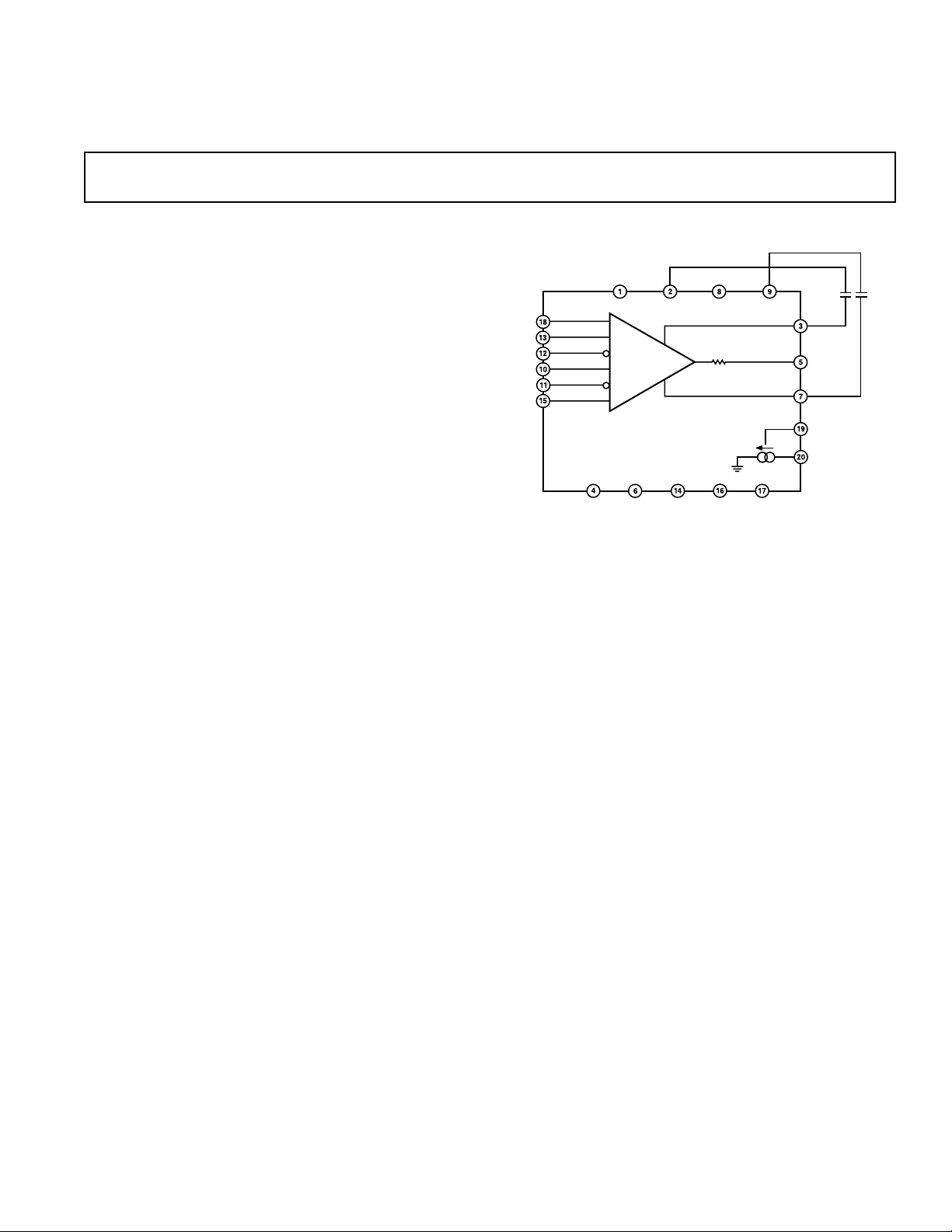
FUNCTIONAL BLOCK DIAGRAM
PRODUCT DESCRIPTION:
The AD53500 is a complete high speed driver designed for use
in digital or mixed signal test systems where high speed and high
output drive capabilities are needed. Combining a high speed
monolithic process and a unique surface mount package, this
product attains superb electrical performance while preserving
optimum packing densities and long-term reliability thanks to an
ultrasmall 20-lead, PSOP package with built-in heat sink.
High and low reference levels can be set within a –2 V to +6 V
range with low offset voltage and high gain accuracy. A 2.5 Ω
output resistance allows use of an external backmatch resistor for
application to 50 Ω, 25 Ω or other complex impedance load
requirements. Without a backmatch resistor it is also capable of
driving highly capacitive loads, typically achieving a rise/fall time
of less than 10 ns with a 1000 pF capacitance. To test I/O
devices, the pin driver can be switched into a high impedance
state (Inhibit Mode), electrically removing the driver from the
path. The pin driver leakage current in inhibit is typically less
than 1 µA and output capacitance is typically less than 18 pF.
Transitions from HI/LO or to inhibit are controlled through the
data and inhibit inputs. The input circuitry utilizes high-speed
differential inputs with a common-mode range of –2 V to +5 V.
This allows for direct interface to the precision of differential
ECL timing or the simplicity of stimulating the pin driver from a
single-ended CMOS or TTL logic source or any combination
over the common-mode range. The analog logic HI/LO inputs
are equally easy to interface, typically requiring 50 µA of bias
current.
REV. 0
Information furnished by Analog Devices is believed to be accurate and
reliable. However, no responsibility is assumed by Analog Devices for its
use, nor for any infringements of patents or other rights of third parties
which may result from its use. No license is granted by implication or
otherwise under any patent or patent rights of Analog Devices.
One Technology Way, P.O. Box 9106, Norwood, MA 02062-9106, U.S.A.
Tel: 781/329-4700 World Wide Web Site: http://www.analog.com
Fax: 781/326-8703 © Analog Devices, Inc., 1999
Page 2
AD53500–SPECIFICATIONS
(All specifications are at TJ = +85ⴗC ⴞ 5ⴗC, +VS = +10 V ⴞ 3%, –VS = +6 V ⴞ 3%
unless otherwise noted. All temperature coefficients are measured over TJ = 75ⴗC–95ⴗC). (In test figures, voltmeter loading is 1 M⍀ or greater,
scope probe loading is 100 k⍀ in parallel with 5 pF.) 39 nF capacitors must be connected between VCC and V
Parameter Min Typ Max Units Test Conditions
DIFFERENTIAL INPUT CHARACTERISTICS
(DATA to DATA, INH to INH)
Common-Mode Input Voltage –2 +5 Volts
Differential Input Range ECL or TTL ECL = –0.8 V/–1.8 V, TTL = 0 V/5 V
Bias Current ±100 µAV
REFERENCE INPUTS
Bias Currents –50 +50 µAV
OUTPUT CHARACTERISTICS
Logic High Range +1 +6 Volts DATA = H, V
Logic Low Range –2 +2 Volts DATA = L, V
Amplitude (V
, VL Interaction –10 +10 mV 100 mV Output Amplitude
V
H
and VL) 0.1 8 Volts VL = –0.05 V, VH = +0.05 V and
H
Absolute Accuracy
Offset –100 +100 mV DATA = H, VH = 0 V, VL = –2 V
V
H
Gain + Linearity Error ±0.3 ±5% of V
V
H
Offset –100 +100 mV DATA = L, VL = 0 V, VH = +6 V
V
L
Gain + Linearity Error ± 0.3 ±5% of V
V
L
Offset TC, V
or V
H
L
0.5 mV/°CV
+ mV DATA = H, VL = –2 V, VH = +1 V to +6 V
H
+ mV DATA = L, VL = –2 V to +2 V, VH = +6 V
L
Output Resistance 1.5 2.5 5.5 Ω V
Dynamic Current Limit 400 mA C
Static Current Limit 60 180 mA Output to –2 V, V
–180 –60 mA DATA = H and Output to +6 V, V
DYNAMIC PERFORMANCE, DRIVE
and VL)
(V
H
Propagation Delay Time 2.5 ns Measured at 50%, V
Propagation Delay TC 1 ps/°C Measured at 50%, V
Delay Matching, Edge-to-Edge 100 ps Measured at 50%, V
Rise and Fall Time
1 V Swing 0.85 ns Measured 20%–80%, V
3 V Swing 2.5 ns Measured 10%–90%, V
5 V Swing 4.0 ns Measured 10%–90%, V
Rise and Fall Time TC
1 V Swing ±1 ps/°C Measured 20%–80%, V
3 V Swing ±2 ps/°C Measured 10%–90%, V
5 V Swing ±3 ps/°C Measured 10%–90%, V
Overshoot, Undershoot and Preshoot +5.0 +30 % of Step + mV V
Settling Time
to 15 mV 40 ns V
to 4 mV 8 µsV
Delay Change vs. Pulsewidth 100 ps V
Minimum Pulsewidth
3 V Swing 3.8 ns V
5 V Swing 5.5 ns V
Toggle Rate 300 MHz VL = –1.8 V, VH = –0.8 V, V
= –2 V, +5 V
CM
, VH = 5 V
L
= –2 V, VH = +6 V
V
L
, VH = 0 V, +5 V and –2 V, 0 V
L
= +3 V, VL = 0 V, I
H
+30 mA
= 39 nF, VH = +5 V, VL = 0 V
BYP
C
LOAD
VL = –2 V, DATA = L
= –400 mV
V
L
= –400 mV
V
L
= –400 mV
V
L
H–VL
= 0 V, VH = 0.5 V
L
= 0 V, VH = 0.5 V
L
= 0 V, VH = 2 V, Pulsewidth = 2.5 ns/
L
Period = 10 ns and Pulsewidth = 30 ns/
Period = 120 ns
= 0 V, VH = 3 V, Output = 2.7 V p-p,
L
Measure at 50%
= 0 V, VH = 5 V, Output = 4.5 V p-p,
L
Measure at 50%
and between VEE and V
HDCPL
= –2 V, VH = +1 V to +6 V
L
= –2 V to +2 V, VH = +6 V
L
= 0, –30 mA,
OUT
= 1000 pF, Tr/Tf = 10 ns
= +6 V, VL = –1 V,
H
= +400 mV,
H
= +400 mV,
H
= +400 mV,
H
= 0 V, VH = 1 V
L
= 0 V, VH = 3 V
L
= 2 V, VH = 3 V
L
= 0 V, VH = 1 V
L
= 0 V, VH = 3 V
L
= 0 V, VH = 5 V
L
= 0.5 V, 1 V, 3 V, 8 V
> 600 mV p-p
OUT
LDCPL
= +6 V,
H
.
–2–
REV. 0
Page 3
Parameter Min Typ Max Units Test Conditions
WARNING!
ESD SENSITIVE DEVICE
DYNAMIC PERFORMANCE, INHIBIT
Delay Time, Active to Inhibit 2 10 ns Measured at 50%, V
= –2 V, 50 Ω Terminated to Ground
V
L
Delay Time, Inhibit to Active 2 10 ns Measured at 50%, V
= –2 V, 50 Ω Terminated to Ground
V
L
I/O Spike <200 mV, p-p V
Output Leakage –1.0 +1.0 µAV
= 0 V, VL = 0 V
H
= –2 V to +6 V
OUT
Output Capacitance 18 pF Driver Inhibited
PSRR, Drive Mode 35 dB VS = V
± 3%
S
POWER SUPPLIES
Total Supply Range 16 V
Positive Supply +10 V
Negative Supply –6 V
Positive Supply Current 85 95 mA
Negative Supply Current 88 98 mA
Total Power Dissipation 1.37 1.54 W
Temperature Sensor Gain Factor 1.0 µA/K R
NOTES
Connecting or shorting the decoupling capacitors to ground will result in the destruction of the device.
Specifications subject to change without notice.
= 10 kΩ, V
LOAD
= +2 V,
H
= +2 V,
H
SOURCE
AD53500
= +10 V
ABSOLUTE MAXIMUM RATINGS
1
Power Supply Voltage
to GND . . . . . . . . . . . . . . . . . . . . . . . . . . . . . . . +11 V
+V
S
to GND . . . . . . . . . . . . . . . . . . . . . . . . . . . . . . . . . –7 V
–V
S
to –VS . . . . . . . . . . . . . . . . . . . . . . . . . . . . . . . . . +18 V
+V
S
Inputs
DATA, DATA, INH, INH . . . . . . . . . . . . . . . . +5 V, –3 V
DATA to DATA, INH to INH . . . . . . . . . . . . . . . . ±3 V
, VL to GND . . . . . . . . . . . . . . . . . . . . . . . . . +7 V, –3 V
V
H
to VL . . . . . . . . . . . . . . . . . . . . . . . . . . . . . . +10 V, 0 V
V
H
Outputs
Short Circuit Duration to Ground . . . . . . . Indefinite
V
OUT
V
Range in Inhibit Mode . . . . . . . . . . . . . See Figure 1
OUT
V
V
. . . . . . . . Do Not Connect Except for Cap to V
HDCPL
. . . . . . . . . Do Not Connect Except for Cap to V
LDCPL
CC
EE
2
3
3
THERM . . . . . . . . . . . . . . . . . . . . . . . . . . . . . . . . +VS, 0 V
Environmental
Operating Temperature (Junction) . . . . . . . . . . . . . .+175°C
Storage Temperature . . . . . . . . . . . . . . . . –65°C to +150°C
Lead Temperature (Soldering, 10 sec)
NOTES
1
Stresses above those listed under Absolute Maximum Ratings may cause perma-
nent damage to the device. This is a stress rating only; functional operation of the
device at these or any other conditions above those indicated in the operational
sections of this specification is not implied. Absolute maximum limits apply
individually, not in combination. Exposure to absolute maximum rating conditions
for extended periods may affect device reliability.
2
Output short circuit protection is guaranteed as long as proper heat sinking is
employed to ensure compliance with the operating temperature limits.
3
The V
dc-current drive capability.
4
To ensure lead coplanarity (±0.002 inches) and solderability, handling with bare
hands should be avoided and the device should be stored in environments at 24°C
± 5°C (75°F ± 10°F) with relative humidity not to exceed 65%.
HDCPL
and V
capacitors may be replaced by a low value resistor for higher
LDCPL
4
. . . . . . . . . . +260°C
V
OUT
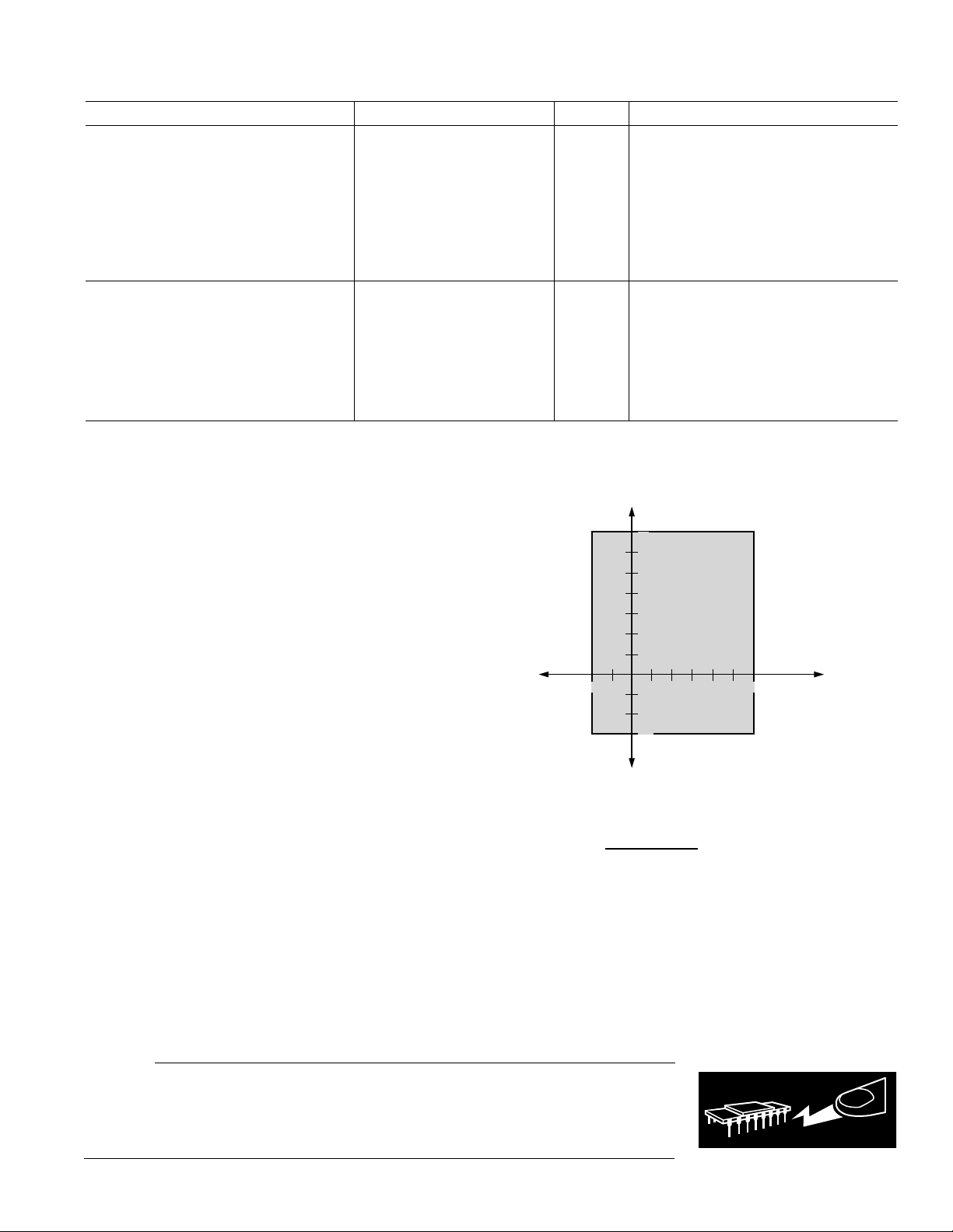
V
= (MAX) = +7V
OUT
7
6
5
4
3
2
1
, V
V
H
–2
V
= (MIN) = –3V
OUT
FIGURE 1 SHOWS THE MAXIMUM ALLOWABLE LIMITS FOR V
OF V
AND V
HIGH
LIMITS, AS STATED BEFORE, ARE MAXIMUM RATINGS ONLY, AND SHOULD NOT
BE USED AS THE PART'S NORMAL OPERATING RANGE. THIS RANGE APPLIES
ONLY TO SUPPLIES OF +VS = +10V AND –VS = –6V AND SHOULD BE DERATED
PROPORTIONALLY FOR LOWER SUPPLIES.
WHEN THE DRIVER IS OPERATING IN INHIBIT MODE. THE
LOW
2345
–1
–2
–3
V
HIGH
/ V
6
OUT
LOW
1
–1
Figure 1. Absolute Maximum Ratings for V
L
AS A FUNCTION
OUT
CAUTION
ESD (electrostatic discharge) sensitive device. Electrostatic charges as high as 4000 V readily
accumulate on the human body and test equipment and can discharge without detection.
Although the AD53500 features proprietary ESD protection circuitry, permanent damage may
occur on devices subjected to high energy electrostatic discharges. Therefore, proper ESD
precautions are recommended to avoid performance degradation or loss of functionality.
REV. 0
–3–
Page 4

AD53500
PIN CONFIGURATION
Table I. Pin Driver Truth Table
Output
V
HDCPL
V
LDCPL
V
V
GND
V
OUT
GND
V
V
INH
CC
CC
EE
EE
10
1
2
3
4
5
AD53500
TOP VIEW
6
(Not to Scale)
7
8
9
20
19
18
17
16
15
14
13
12
11
THERM
TV
CC
V
H
GND
GND
V
L
GND
DATA
DATA
INH
DATA DATA INH INH State
0101V
1001V
L
H
0110Hi-Z
1010Hi-Z
Table II. Package Thermal Characteristics
Air Flow, FM JC, ⴗC/W JA, ⴗC/W
50 3.28 49.1
400 3.91 33.74
PIN FUNCTION DESCRIPTIONS
Pin Name Pin Number Description
V
CC
1, 2 Positive Power Supply. Both pins should be connected to minimize inductance and allow
maximum speed of operation. V
should be decoupled to GND with a low inductance
CC
0.1 µF capacitor.
V
EE
8, 9 Negative Power Supply. Both pins should be connected to keep the inductance down and
allow maximum speed of operation. V
should be decoupled to GND with a low inductance
EE
0.1 µF capacitor.
GND 4, 6, 14, 16, 17 Device Ground. These pins should be connected to the circuit board’s ground plane at the
pins.
V
L
15 Analog input that sets the voltage level of a Logic 0 of the driver. Determines the driver out-
put for DATA > DATA.
V
H
18 Analog input that sets the voltage level of a Logic 1 of the driver. Determines the driver out-
put for DATA > DATA.
V
OUT
V
HDCPL
5 The Driver Output.
3 Internal supply decoupling for the output stage. This pin is connected to VCC through a
39 nF (minimum) capacitor.
V
LDCPL
7 Internal supply decoupling for the output stage. This pin is connected to VEE through a
39 nF (minimum) capacitor.
INH, INH 10, 11 Differential inputs that control the high impedance state of the driver. When INH > INH, the
driver goes into a high impedance state.
DATA, DATA 13, 12 Differential inputs that determine the high and low state of the driver. Driver output is high
for DATA > DATA.
TV
CC
19 Temperature Sensor Startup Pin. This pin should be connected to VCC.
THERM 20 Temperature sensor output pin. A resistor (10 kΩ) should be connected between THERM
and V
. The approximate die temperature can be determined by measuring the current
CC
through the resistor. The typical scale factor is 1 µA/K.
ORDERING GUIDE
Shipment Method,
Package Quantity Per Package
Model Description Shipping Container Option
AD53500JRP 20-Lead Power SOIC Tube, 38 Pieces RP-20
–4–
REV. 0
Page 5

AD53500
RISING-EDGE SLEW
CONTROL CURRENT
5V
V+
V
HDCPL
LEVEL-SHIFTED
LOGIC DRIVE
V
H
V–
Q49
OUT
Q50
Q48
APPLICATION INFORMATION
Power Supply Distribution, Bypassing and Sequencing
The AD53500 draws substantial transient currents from its
power supplies when switching between states and careful design of the power distribution and bypassing is key to obtaining
specified performance. Supplies should be distributed using
broad, low inductance traces or (preferably) planes in a multilayered board with a dedicated ground-plane layer. All of the
device’s power supply pins should be used to minimize the internal inductance presented by the part’s bond wires. Each supply
must be bypassed to ground with at least one 0.1 µF capacitor;
chip-style capacitors are preferable as they minimize inductance.
One or more 10 µF (or greater) Tantalum capacitors per board
are also advisable to provide additional local energy storage.
The AD53500’s current-limit circuitry also requires external
bypass capacitors. Figure 2 shows a simplified schematic of the
positive current-limit circuit. Excessive collector current in
output transistor Q49 creates a voltage drop across the 5 Ω
resistor, which turns on PNP transistor Q48. Q48 diverts the
rising-edge slew current, shutting down the current mirror and
removing the output stage’s base drive. The V
HDCPL
pin should
be bypassed to the positive supply with a 0.039 µF capacitor,
while the V
pin (not shown) requires a similar capacitor to
LDCPL
the negative supply. These capacitors ensure that the AD53500
does not current-limit during normal output transitions up its
full 8 V rated step size. Both capacitors must have minimumlength connections to the AD53500. Here again, chip capacitors
are ideal.
Several points about the current-limit circuitry should be noted.
First, the limiting currents are not tightly controlled, as they are
functions of both absolute transistor V
and junction tempera-
BE
ture; higher dc output current is available at lower junction
temperatures. Second, it is essential to connect the V
HDCPL
capacitor to the positive supply (and the V
capacitor to the
LDCPL
negative supply)—failure to do so causes considerable thermal
stress in the current-limiting resistor(s) during normal supply
sequencing and may ultimately cause them to fail, rendering the
part nonfunctional. Finally, the AD53500 may appear to function normally for small output steps (less than 3 V or so) if one
or both of these caps is absent, but it may exhibit excessive rise
or fall times for steps of larger amplitude.
The AD53500 does not require special power-supply sequencing. However, good design practice dictates that digital and
analog control signals not be applied to the part before the supplies are stable. Violating this guideline will not normally destroy the part, but the active inputs can draw considerable
current until the main supplies are applied.
Figure 2. Simplified Schematic of the AD53500 Output
Stage and Positive Current-Limit Circuitry
REV. 0
–5–
Page 6

AD53500
J7
SIDE SMA
R8
47V
50V
V
OUT
C20
1000pF
C3
C17
C16
0.039mF
3
4
5
6
7
C19
S
+V
0.1mF
IL+
OUT
V
0.039mF
IL–
U3
AD53500
H
L
THV
19 17 1 2
C2
0.1mF
H
V
L
V
C1
0.1mF
50V
SMA
J4
THERM
50V
SMA
J3
C14
0.1mF
R3
50V
V
13*1210*
18
15
20
50V
SMA
J5
DATA
INH
16 14 9 8
11
50V
SMA
J6
C15
0.1mF
R2
50V
0.1mF
S
–V
–5.2V
EE
V
GND
CC
V
C11
0.1mF
C10
0.1mF
C9
0.1mF
VL–2V
VH–VSTHERM
LINE.
OUT
TO BE MOUNTED ON ITS SIDE FOR BEST IMPEDANCE
OUT
NOTES:
1. 50V TERMINATION TO BE AS CLOSE TO RECEIVER AS POSSIBLE.
(END OF TRACE MARKED BY *). THROUGH SMA CONNECTS BETWEEN
MC10EL16 OUTPUTS AND DUT.
2. NO VIAS ALLOWED ON V
3. SMA ON V
MATCH.
4. ONE DIMENSION OF BOARD TO BE 4 1/2 INCHES.
5. DUT PACKAGE IS TO BE CENTERED ON BOARD.
6. ALL RESISTORS AND NONELECTROLYTIC CAPS ARE 0805-SIZE
SURFACE MOUNT.
7. SEE DATA FOR HIDDEN POWER AND GROUND PINS ON LOGIC GATES.
8. ALL 100nF BYPASS CAPACITORS TO BE LOCATED CLOSE TO PACKAGE.
9. PCB IS TO BE FOUR-LAYER WITH POWER GND ( ) AND –2V AS INNER
PLANES.
S
–5.2V
+V
C8
0.1mF
C5
1mF
C6
1mF
7
U1
MC10EL16
98
2
50V
J1
SMA
R6
DATA
C7
R1
–5.2V
45
50V
C22
C13
S
GND
1
TP
JP1
–2V
0.1mF
0.01mF
JP2
S
–V
+V
1
1
TP
TP
JP3
192103114125136147158
P1
R4
50V
–5.2V
6
45
3
50V
C21
C12
–2V
0.1mF
0.01mF
7
U2
MC10EL16
98
2
50V
J2
SMA
INH
6
3
R5
50V
1mF
C4
1mF
DB15
Figure 3. Evaluation Board Schematic
–6–
REV. 0
Page 7

OUTLINE DIMENSIONS
SEATING
PLANE
0.0118 (0.30)
0.0040 (0.10)
0.0201 (0.51)
0.0130 (0.33)
0.1043 (2.65)
0.0926 (2.35)
0.0500
(1.27)
BSC
STANDOFF
0.0500 (1.27)
0.0057 (0.40)
88
08
0.0295 (0.75)
0.0098 (0.25)
3 458
0.5118 (13.00)
0.4961 (12.60)
0.4193 (10.65)
0.3937 (10.00)
0.2992 (7.60)
0.2914 (7.40)
PIN 1
0.3340 (8.61)
0.3287 (8.35)
0.1890 (4.80)
0.1791 (4.55)
20
1
11
10
HEAT
SINK
Dimensions shown in inches and (mm).
20-Lead Thermally Enhanced Small Outline Package (PSOP)
(RP-20)
AD53500
C3527–2–4/99
REV. 0
PRINTED IN U.S.A.
–7–
 Loading...