

Page 1
2.5 V to 5.5 V, 400 μA, 2-Wire Interface,
Quad Voltage Output, 8-/10-/12-Bit DACs
FEATURES
AD5306: 4 buffered, 8-bit DACs in 16-lead TSSOP
A version: ±1 LSB INL; B version: ±0.625 LSB INL
AD5316: 4 buffered, 10-bit DACs in 16-lead TSSOP
A version: ±4 LSB INL; B version: ±2.5 LSB INL
AD5326: 4 buffered, 12-bit DACs in 16-lead TSSOP
A version: ±16 LSB INL; B version: ±10 LSB INL
Low power operation: 400 μA @ 3 V, 500 μA @ 5 V
2-wire (I
2.5 V to 5.5 V power supply
Guaranteed monotonic by design over all codes
Power-down to 90 nA @ 3 V, 300 nA @ 5 V (
Double-buffered input logic
Buffered/unbuffered reference input options
Output range: 0 V to V
Power-on reset to 0 V
Simultaneous update of outputs (
Software clear facility
Data readback facility
On-chip rail-to-rail output buffer amplifiers
Temperature range −40°C to +105°C
APPLICATIONS
Portable battery-powered instruments
Digital gain and offset adjustment
Programmable voltage and current sources
Programmable attenuators
Industrial process control
1
Protected by U.S. Patent Numbers 5,969,657 and 5,684,481.
Rev. F
Information furnished by Analog Devices is believed to be accurate and reliable.
However, no responsibility is assumed by Analog Devices for its use, nor for any
infringements of patents or other rights of third parties that may result from its use.
Specifications subject to change without notice. No license is granted by implication
or otherwise under any patent or patent rights of Analog Devices. Trademarks and
registered trademarks are the property of their respective owners.
2
C®-compatible) serial interface
or 0 V to 2 V
REF
LDAC
REF
pin)
pin or bit)
PD
AD5306/AD5316/AD5326
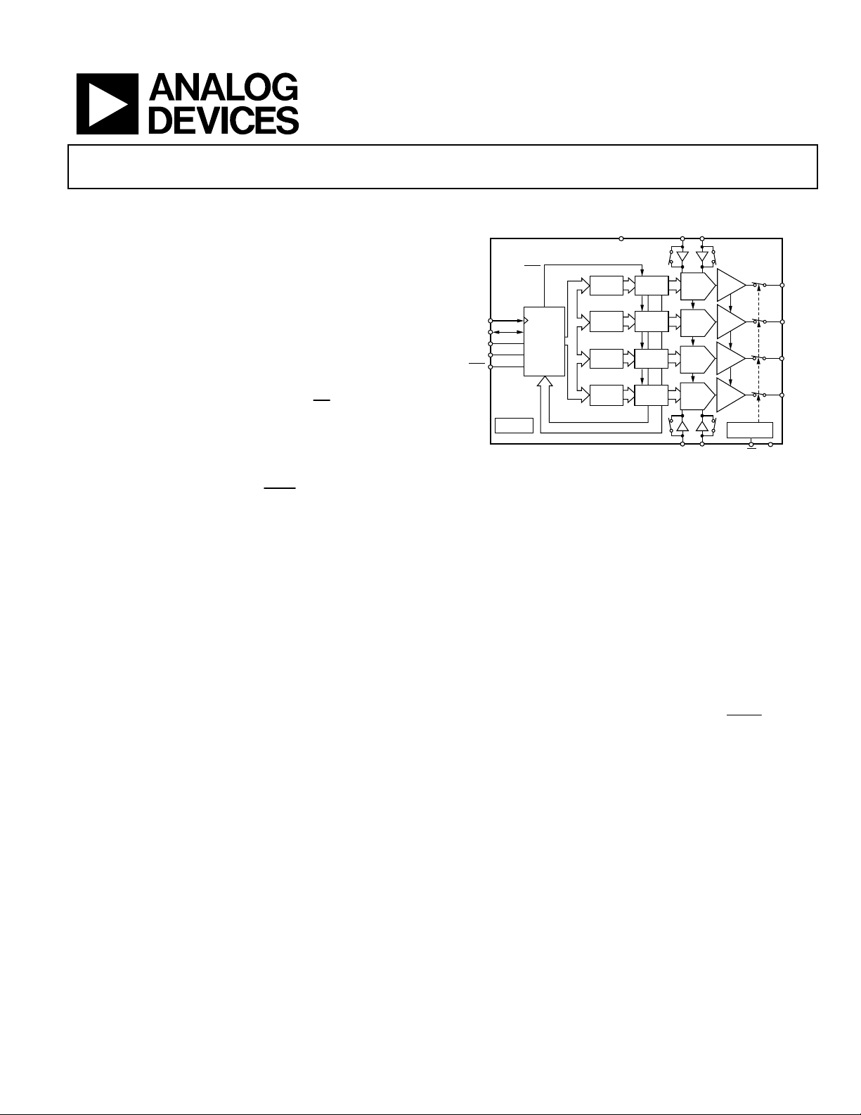
FUNCTIONAL BLOCK DIAGRAM
V
BV
DAC
DAC
DAC
DAC
REF
REF
A
STRING
DAC A
STRING
DAC B
STRING
DAC C
STRING
DAC D
D
V
REF
REF
BUFFER
BUFFER
BUFFER
BUFFER
POWER-DOWN
CV
LDAC
V
DD
AD5306/AD5316/AD5326
LDAC
SCL
SDA
A1
A0
POWER-ON
RESET
LDAC
INTERFACE
LOGIC
INPUT
REGISTER
INPUT
REGISTER
INPUT
REGISTER
INPUT
REGISTER
REGISTER
REGISTER
REGISTER
REGISTER
Figure 1.
GENERAL DESCRIPTION
The AD5306/AD5316/AD53261 are quad 8-/10-/12-bit buffered
voltage output DACs in 16-lead TSSOP packages that operate
from a single 2.5 V to 5.5 V supply, consuming 500 μA at 3 V.
Their on-chip output amplifiers allow rail-to-rail output swing
with a slew rate of 0.7 V/μs. A 2-wire serial interface, which
operates at clock rates up to 400 kHz, is used. This interface is
SMBus-compatible at V
placed on the same bus.
Each DAC has a separate reference input that can be configured
as buffered or unbuffered. The outputs of all DACs can be
updated simultaneously using the asynchronous
The parts incorporate a power-on reset circuit that ensures the
DAC outputs power up to 0 V and remain there until a valid
write to the device takes place. The software clear function
clears all DACs to 0 V. The parts contain a power-down feature
that reduces the current consumption of the device to
300 nA @ 5 V (90 nA @ 3 V).
All three parts have the same pinout, which allows users to select
the amount of resolution appropriate for their application without
redesigning their circuit board.
One Technology Way, P.O. Box 9106, Norwood, MA 02062-9106, U.S.A.
Tel: 781.329.4700 www.analog.com
Fax: 781.461.3113 © 2005 Analog Devices, Inc. All rights reserved.
< 3.6 V. Multiple devices can be
DD
LOGIC
V
V
V
V
GNDPD
input.
A
OUT
B
OUT
C
OUT
D
OUT
02066-001
Page 2

AD5306/AD5316/AD5326
TABLE OF CONTENTS
Specifications..................................................................................... 3
AC Characteristics........................................................................ 5
Timing Characteristics ................................................................ 6
Absolute Maximum Ratings............................................................ 7
ESD Caution.................................................................................. 7
Pin Configuration and Function Descriptions............................. 8
Te r mi n ol o g y ...................................................................................... 9
Typical Performance Characteristics ........................................... 11
Functional Description .................................................................. 15
Digital-to-Analog Section ......................................................... 15
Resistor String............................................................................. 15
DAC Reference Inputs ............................................................... 15
Output Amplifier........................................................................ 15
Power-On Reset .......................................................................... 16
Serial Interface............................................................................ 16
Read/Write Sequence................................................................. 16
Pointer Byte Bits ......................................................................... 16
Input Shift Register..................................................................... 16
Default Readback Conditions................................................... 17
Multiple DAC Write Sequence ................................................. 17
Multiple DAC Readback Sequence .......................................... 17
Write Operation.......................................................................... 18
Read Operation........................................................................... 18
Double-Buffered Interface........................................................ 19
Load DAC Input
Power-Down Mode .................................................................... 19
Applications..................................................................................... 20
Typical Application C i r c uit ....................................................... 20
Driving V
Bipolar Operation Using the AD5306/AD5316/AD5326..... 20
Multiple Devices on One Bus ................................................... 20
AD5306/AD5316/AD5326 as a Digitally Programmable
Window Detector....................................................................... 21
Coarse and Fine Adjustment Using the
AD5306/AD5316/AD5326 ....................................................... 21
Power Supply Decoupling ............................................................. 22
Outline Dimensions ....................................................................... 24
Ordering Guide .......................................................................... 24
LDAC
............................................................. 19
from the Reference Voltage ................................ 20
DD
REVISION HISTORY
8/05—Rev. E to Rev. F
Replaced Figure 22 .........................................................................13
Changes to Bipolar Operation
Using the AD5306/AD5316/AD5326 Section........................ 20
Changes to Ordering Guide.......................................................... 24
5/05—Rev. D to Rev. E
Changes to Table 1............................................................................ 3
11/04—Rev. C to Rev. D
Change to Figure 31 ....................................................................... 16
Changes to Pointer Byte Section................................................... 16
Change to Figure 32 ....................................................................... 17
Rev. F | Page 2 of 24
8/03—Rev. B to Rev. C
Added A Version ................................................................Universal
Changes to FEATURES ....................................................................1
Changes to SPECIFICATIONS .......................................................2
Changes to ABSOLUTE MAXIMUM RATINGS .........................5
Edits to ORDERING GUIDE ..........................................................5
Changes to TPC 21......................................................................... 11
Added OCTALS section to Table I............................................... 18
Updated OUTLINE DIMENSIONS ............................................ 19
4/01—Rev. A to Rev. B
Edit to Figure 6 ............................................................................... 13
Edits to RIGHT/LEFT section of Pointer Byte Bits section...... 13
Edits to Input Shift Register section ............................................ 13
Edits to Figure 7.............................................................................. 13
Edits to Figure 8.............................................................................. 14
Edits to Figure 9.............................................................................. 14
Edit to Figure 12 ............................................................................. 16
2/01—Rev. 0 to Rev. A
6/00—Revision 0: Initial Version
Page 3

AD5306/AD5316/AD5326
SPECIFICATIONS
VDD = 2.5 V to 5.5 V; V
Table 1.
A Version
Parameter
DC PERFORMANCE
DAC REFERENCE INPUTS
OUTPUT CHARACTERISTICS
2
3, 4
AD5306
Resolution 8 8 Bits
Relative Accuracy ±0.15 ±1 ±0.15 ±0.625 LSB
Differential Nonlinearity ±0.02 ±0.25 ±0.02 ±0.25 LSB Guaranteed monotonic by
AD5316
Resolution 10 10 Bits
Relative Accuracy ±0.5 ±4 ±0.5 ±2.5 LSB
Differential Nonlinearity ±0.05 ±0.5 ±0.05 ±0.5 LSB Guaranteed monotonic by
AD5326
Resolution 12 12 Bits
Relative Accuracy ±2 ±16 ±2 ±10 LSB
Differential Nonlinearity ±0.2 ±1 ±0.2 ±1 LSB Guaranteed monotonic by
Offset Error ±5 ±60 ±5 ±60 mV VDD = 4.5 V, gain = 2;
Gain Error ±0.3 ±1.25 ±0.3 ±1.25 % of FSR VDD = 4.5 V, gain = 2;
Lower Deadband
Upper Deadband
Offset Error Drift
Gain Error Drift
6
6
DC Power Supply
Rejection Ratio
DC Crosstalk
V
REF
6
Input Range 1 V
0.25 V
V
Input Impedance >10 >10 MΩ Buffered reference mode
REF
148 180 148 180 kΩ Unbuffered reference mode;
74 90 74 90 kΩ Unbuffered reference mode;
Reference Feedthrough −90 −90 dB Frequency = 10 kHz.
Channel-to-Channel Isolation −75 −75 dB Frequency = 10 kHz.
Minimum Output Voltage
Maximum Output Voltage
DC Output Impedance 0.5 0.5 Ω
= 2 V; RL = 2 kΩ to GND; CL = 200 pF to GND; all specifications T
REF
1
Min Typ Max Min Typ Max Unit Conditions/Comments
5
5
10 60 10 60 mV See Figure 4; lower
10 60 10 60 mV See Figure 5; upper
−12 –12 ppm of FSR/°C
–5 –5 ppm of FSR/°C
6
–60 –60 dB ΔVDD = ±10%.
200 200 μV RL = 2 kΩ to GND or V
6
DD
DD
6
7
0.001 0.001 V This is a measure of the
7
V
− 0.001 VDD − 0.001 V
DD
1 V
0.25 V
B Version
to T
MIN
1
, unless otherwise noted.
MAX
design over all codes.
design over all codes.
design over all codes.
Figure 4 and Figure 5.
see
Figure 4 and Figure 5.
see
deadband exists only if
offset error is negative.
deadband exists only if
V
= VDD and offset plus
REF
gain error is positive.
DD.
DD
DD
V Buffered reference mode.
V Unbuffered reference mode.
and power-down mode.
0 V to V
0 V to 2 V
output range.
REF
output range.
REF
minimum and maximum
drive capability of the
output amplifier.
Rev. F | Page 3 of 24
Page 4

AD5306/AD5316/AD5326
A Version
Parameter
2
Min Typ Max Min Typ Max Unit Conditions/Comments
1
B Version
1
Short-Circuit Current 25 25 mA VDD = 5 V.
16 16 mA VDD = 3 V.
Power-Up Time 2.5 2.5 μs Coming out of power-
down mode; V
= 5 V.
DD
5 5 μs Coming out of power-
= 3 V.
DD
LOGIC INPUTS
(Excluding SCL, SDA)
down mode; V
6
Input Current ±1 ±1 μA
VIL, Input Low Voltage 0.8 0.8 V VDD = 5 V ± 10%.
0.6 0.6 V VDD = 3 V ± 10%.
0.5 0.5 V VDD = 2.5 V.
VIH, Input High Voltage 1.7 1.7 V VDD = 2.5 V to 5.5 V;
TTL and 1.8 V CMOS
compatible.
Pin Capacitance 3 3 pF
LOGIC INPUTS (SCL, SDA)6
VIH, Input High Voltage 0.7 V
VIL, Input Low Voltage −0.3 +0.3 V
V
DD
+ 0.3 0.7 V
DD
DD
V
DD
+ 0.3 V SMBus compatible at
DD
V
DD
< 3.6 V.
−0.3 +0.3 VDDV SMBus compatible at
< 3.6 V.
V
DD
IIN, Input Leakage Current ±1 ±1 μA
V
, Input Hysteresis 0.05 VDD 0.05 VDD V See Figure 20.
HYST
CIN, Input Capacitance 8 8 pF
Glitch Rejection 50 50 ns Input filtering suppresses
noise spikes of less than
50 ns.
LOGIC OUTPUT (SDA)6
VOL, Output Low Voltage 0.4 0.4 V I
0.6 0.6 V I
= 3 mA.
SINK
= 6 mA.
SINK
Three-State Leakage Current ±1 ±1 μA
Three-State Output
8 8 pF
Capacitance
POWER REQUIREMENTS
V
DD
IDD (Normal Mode)
8
2.5 5.5 2.5 5.5 V
V
= VDD and VIL = GND;
IH
interface inactive.
VDD = 4.5 V to 5.5 V 500 900 500 900 μA All DACs in unbuffered
mode.
Buffered mode, extra
current is typically x mA
per DAC, where
x = 5 μA + V
REF/RDAC.
VDD = 2.5 V to 3.6 V 400 750 400 750 μA
IDD (Power-Down Mode) VIH = VDD and VIL = GND;
interface inactive.
VDD = 4.5 V to 5.5 V 0.3 1 0.3 1 μA IDD = 3 μA (max) during
readback on SDA.
VDD = 2.5 V to 3.6 V 0.09 1 0.09 1 μA IDD = 1.5 μA (max) during
readback on SDA.
1
Temperature range (A, B versions): −40°C to +105°C; typical at +25°C.
2
See the Terminology section.
3
DC specifications tested with the outputs unloaded.
4
Linearity is tested using a reduced code range: AD5306 (Code 8 to 255); AD5316 (Code 28 to 1023); AD5326 (Code 115 to 4095).
5
This corresponds to x codes. x = deadband voltage/LSB size.
6
Guaranteed by design and characterization; not production tested.
7
For the amplifier output to reach its minimum voltage, the offset error must be negative; for the amplifier output to reach its maximum voltage, V
the offset plus gain error must be positive.
8
Interface inactive; all DACs active. DAC outputs unloaded.
= VDD,
REF
Rev. F | Page 4 of 24
Page 5

AD5306/AD5316/AD5326
AC CHARACTERISTICS
VDD = 2.5 V to 5.5 V; RL = 2 kΩ to GND; CL = 200 pF to GND; all specifications T
Table 2.
A, B Versions
Parameter
3
Min Typ Max Unit Conditions/Comments
1, 2
Output Voltage Settling Time V
AD5306 6 8 μs 1/4 scale to 3/4 scale change (0x40 to 0xC0)
AD5316 7 9 μs 1/4 scale to 3/4 scale change (0x100 to 0x300)
AD5326 8 10 μs 1/4 scale to 3/4 scale change (0x400 to 0xC00)
Slew Rate 0.7 V/μs
Major-Code Change Glitch Energy 12 nV-s 1 LSB change around major carry
Digital Feedthrough 0.5 nV-s
Digital Crosstalk 0.5 nV-s
Analog Crosstalk 1 nV-s
DAC-to-DAC Crosstalk 3 nV-s
Multiplying Bandwidth 200 kHz V
Total Harmonic Distortion −70 dB V
1
Guaranteed by design and characterization; not production tested.
2
Temperature range (A, B versions): −40°C to +105°C; typical at +25°C.
3
See the Terminology section.
MIN
to T
, unless otherwise noted.
MAX
= VDD = 5 V
REF
= 2 V ± 0.1 V p-p, unbuffered mode
REF
= 2.5 V ± 0.1 V p-p, frequency = 10 kHz
REF
Rev. F | Page 5 of 24
Page 6
AD5306/AD5316/AD5326
A
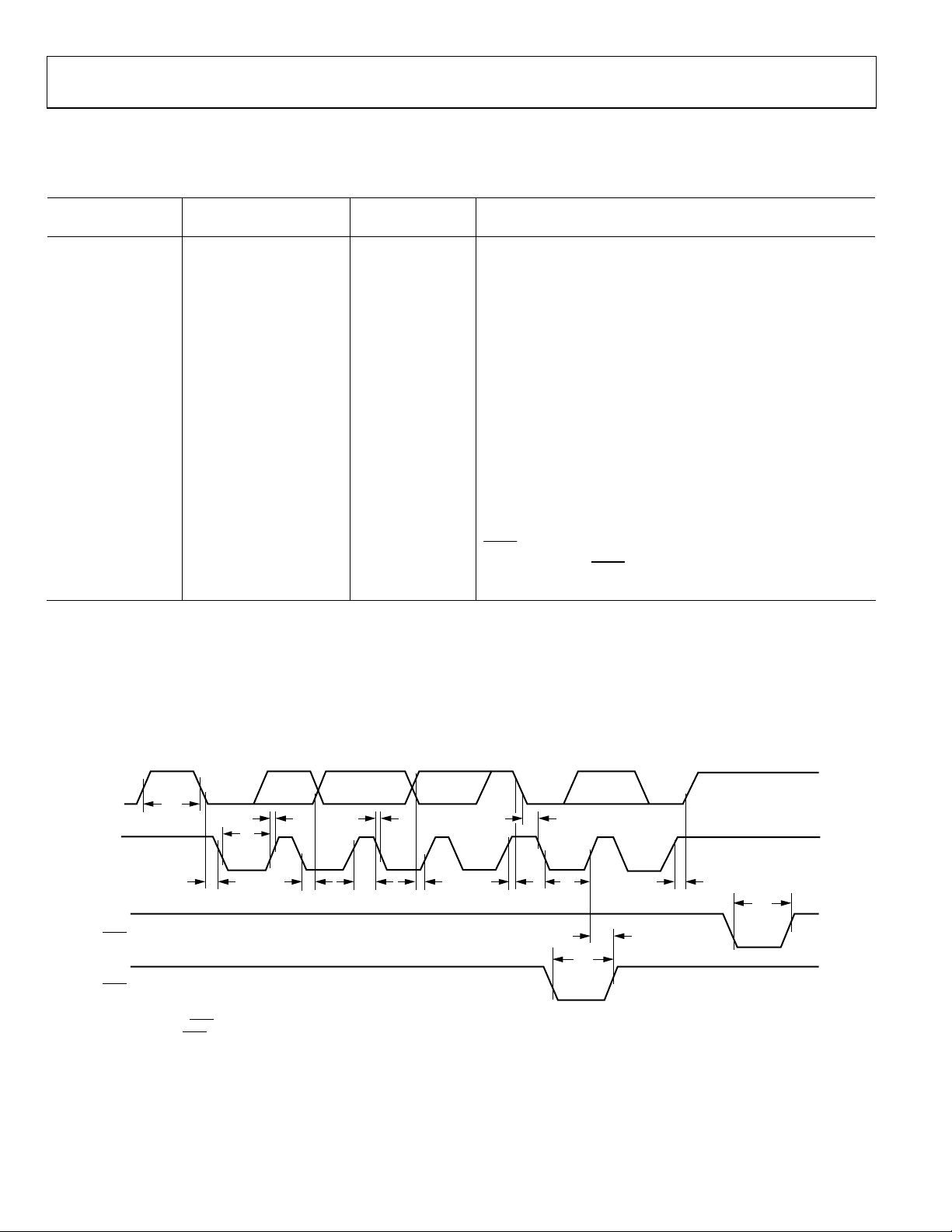
TIMING CHARACTERISTICS
VDD = 2.5 V to 5.5 V; all specifications T
Table 3.
Parameter
t
1
t
2
t
3
t
4
t
5
3
t
6
2
0 μs min
t
7
t
8
t
9
t
10
0 ns min tR, rise time of SCL and SDA when receiving (CMOS compatible)
t
11
0 ns min tF, fall time of SDA when receiving (CMOS compatible)
300 ns max tF, fall time of SCL and SDA when receiving
20 + 0.1C
t
12
t
13
4
C
B
1
See Figure 2.
2
Guaranteed by design and characterization; not production tested.
3
A master device must provide a hold time of at least 300 ns for the SDA signal (referred to the VIH min of the SCL signal) to bridge the undefined region of SCL’s
falling edge.
4
CB is the total capacitance of one bus line in pF. tR and tF measured between 0.3 VDD and 0.7 VDD.
Limit at T
2.5 μs min SCL cycle time
0.6 μs min t
1.3 μs min t
0.6 μs min t
100 ns min t
0.9 μs max t
0.6 μs min t
0.6 μs min t
1.3 μs min t
300 ns max tR, rise time of SCL and SDA when receiving
250 ns max tF, fall time of SDA when transmitting
20 ns min
400 ns min
400 pF max Capacitive load for each bus line
1
MIN
A, B Versions
, T
MIN
MAX
4
B
to T
, unless otherwise noted.
MAX
Unit Conditions/Comments
, SCL high time
HIGH
, SCL low time
LOW
, start/repeated start condition hold time
HD,STA
, data setup time
SU,DAT
, data hold time
HD,DAT
, setup time for repeated start
SU,STA
, stop condition setup time
SU,STO
, bus free time between a stop and a start condition
BUF
ns min tF, fall time of SCL and SDA when transmitting
LDAC pulse width
SCL rising edge to
LDAC rising edge
START
CONDITION
SD
t
9
t
3
SCL
t
4
1
LDAC
2
LDAC
NOTES
1
ASYNCHRONOUS LDAC UPDATE MODE.
2
SYNCHRONOUS LDAC UPDATE MODE.
t
10
t
6
t
11
t
2
t
5
Figure 2. 2-Wire Serial Interface Timing Diagram
REPEATED START
CONDITION
t
4
t
7
STOP
CONDITION
t
1
t
13
t
12
t
8
t
12
02066-002
Rev. F | Page 6 of 24
Page 7
AD5306/AD5316/AD5326
ABSOLUTE MAXIMUM RATINGS
TA = 25°C, unless otherwise noted.
Table 4.
Parameter
VDD to GND −0.3 V to +7 V
SCL, SDA to GND −0.3 V to VDD + 0.3 V
A0, A1, LDAC, PD to GND
Reference Input Voltage to GND −0.3 V to VDD + 0.3 V
V
OUT
Operating Temperature Range
Industrial (A, B Versions) −40°C to +105°C
Storage Temperature Range −65°C to +150°C
Junction Temperature (TJ max) 150°C
16-Lead TSSOP
Power Dissipation (TJ max − TA)/θ
θJA Thermal Impedance 150.4°C/W
Reflow Soldering
Peak Temperature 220°C
Time at Peak Temperature 10 sec to 40 sec
1
Transient currents of up to 100 mA do not cause SCR latch-up.
A to V
1
D to GND −0.3 V to VDD + 0.3 V
OUT
Value
−0.3 V to V
+ 0.3 V
DD
JA
Stresses above those listed under Absolute Maximum Ratings
may cause permanent damage to the device. This is a stress
rating only; functional operation of the device at these or any
other conditions above those indicated in the operational
section of this specification is not implied. Exposure to absolute
maximum rating conditions for extended periods may affect
device reliability.
ESD CAUTION
ESD (electrostatic discharge) sensitive device. Electrostatic charges as high as 4000 V readily accumulate on the
human body and test equipment and can discharge without detection. Although this product features
proprietary ESD protection circuitry, permanent damage may occur on devices subjected to high energy
electrostatic discharges. Therefore, proper ESD precautions are recommended to avoid performance
degradation or loss of functionality.
Rev. F | Page 7 of 24
Page 8
AD5306/AD5316/AD5326
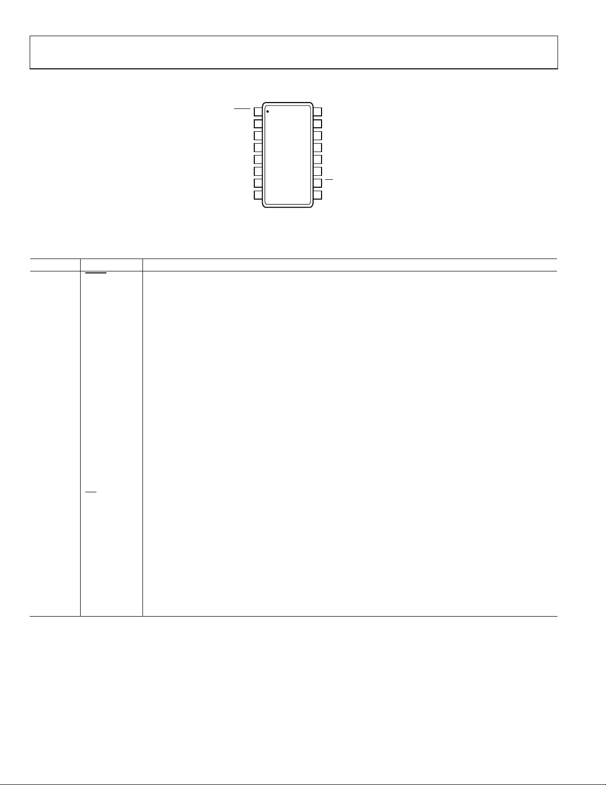
PIN CONFIGURATION AND FUNCTION DESCRIPTIONS
1
LDAC
2
V
DD
3
V
A
OUT
V
OUT
V
OUT
V
REF
V
REF
V
REF
AD5306/
4
AD5316/
B
AD5326
5
C
TOP VIEW
(Not to Scale)
6
A
7
B
8
CV
16
A1
15
A0
14
SCL
13
SDA
12
GND
11
D
V
OUT
10
PD
9
D
REF
02066-003
Figure 3. Pin Configuration
Table 5. Pin Function Descriptions
Pin No. Mnemonic Description
1
LDAC
Active Low Control Input. Transfers the contents of the input registers to their respective DAC registers.
Pulsing this pin low allows any or all DAC registers to be updated if the input registers have new data. This
allows simultaneous update of all DAC outputs. Alternatively, this pin can be tied permanently low.
2 V
DD
Power Supply Input. These parts can be operated from 2.5 V to 5.5 V and the supply should be decoupled
with a10 μF capacitor in parallel with a 0.1 μF capacitor to GND.
3 V
4 V
5 V
6 V
A Buffered Analog Output Voltage from DAC A. The output amplifier has rail-to-rail operation.
OUT
B Buffered Analog Output Voltage from DAC B. The output amplifier has rail-to-rail operation.
OUT
C Buffered Analog Output Voltage from DAC C. The output amplifier has rail-to-rail operation.
OUT
REF
A
Reference Input Pin for DAC A. This pin can be configured as a buffered or an unbuffered input depending on
the state of the BUF bit in the input word to DAC A. It has an input range from 0.25 V to V
7 V
REF
mode and from 1 V to V
B
Reference Input Pin for DAC B. This pin can be configured as a buffered or an unbuffered input depending on
in buffered mode.
DD
the state of the BUF bit in the input word to DAC B. It has an input range from 0.25 V to V
8 V
REF
mode and from 1 V to V
C
Reference Input Pin for DAC C. This pin can be configured as a buffered or an unbuffered input depending on
in buffered mode.
DD
the state of the BUF bit in the input word to DAC C. It has an input range from 0.25 V to V
9 V
REF
mode and from 1 V to V
D
Reference Input Pin for DAC D. This pin can be configured as a buffered or an unbuffered input depending on
in buffered mode.
DD
the state of the BUF bit in the input word to DAC D. It has an input range from 0.25 V to V
in buffered mode.
DD
10
mode and from 1 V to V
PD Active Low Control Input. Acts as a hardware power-down option. All DACs go into power-down mode when
this pin is tied low. The DAC outputs go into a high impedance state. The current consumption of the part
drops to 300 nA @ 5 V (90 nA @ 3 V).
11 V
D Buffered Analog Output Voltage from DAC D. The output amplifier has rail-to-rail operation.
OUT
12 GND Ground Reference Point for All Circuitry on the Part.
13 SDA
Serial Data Line. This is used in conjunction with the SCL line to clock data into the 16-bit input shift register.
It is a bidirectional open-drain data line that should be pulled to the supply with an external pull-up resistor.
14 SCL
Serial Clock Line. This is used in conjunction with the SDA line to clock data into the 16-bit input shift register.
Clock rates of up to 400 kbps can be accommodated in the I
15 A0 Address Input. Sets the LSB of the 7-bit slave address.
16 A1 Address Input. Sets the second LSB of the 7-bit slave address.
2
C-compatible interface.
in unbuffered
DD
in unbuffered
DD
in unbuffered
DD
in unbuffered
DD
Rev. F | Page 8 of 24
Page 9

AD5306/AD5316/AD5326
TERMINOLOGY
Relative Accuracy or Integral Nonlinearity (INL)
For the DAC, it is a measure, in LSB, of the maximum deviation
from a straight line passing through the endpoints of the DAC
transfer function. Typical INL vs. code plots are shown in
Figure 6, Figure 7, and Figure 8.
Differential Nonlinearity (DNL)
The difference between the measured change and the ideal 1 LSB
change between any two adjacent codes. A specified differential
nonlinearity of 1 LSB maximum ensures monotonicity. This DAC
is guaranteed monotonic by design. Typical DNL vs. code plots
are shown in
Figure 9, Figure 10, and Figure 11.
Offset Error
A measure of the offset error of the DAC and the output amplifier. It can be positive or negative. See
Figure 4 and Figure 5.
Offset error is expressed in mV.
Gain Error
A measure of the span error of the DAC. It is the deviation in
slope of the actual DAC transfer characteristic from the ideal
expressed as a percentage of the full-scale range.
Offset Error Drift
A measure of the change in offset error with changes in
temperature. Offset error drift is expressed in (ppm of full-scale
range)/°C.
Gain Error Drift
A measure of the change in gain error with changes in
temperature. Gain error drift is expressed in (ppm of full-scale
range)/°C.
DC Power Supply Rejection Ratio (PSRR)
This indicates how the output of the DAC is affected by changes
in the supply voltage. PSRR is the ratio of the change in V
a change in V
measured in dB. V
for full-scale output of the DAC. PSRR is
DD
is held at 2 V and VDD is varied 10%.
REF
OUT
to
DC Crosstalk
The dc change in the output level of one DAC at midscale in
response to a full-scale code change (all 0s to all 1s, and vice
versa) and output change of another DAC. DC crosstalk is
expressed in μV.
Reference Feedthrough
The ratio of the amplitude of the signal at the DAC output to
the reference input when the DAC output is not being updated,
that is, when
is high. Reference feedthrough is expressed
LDAC
in dB.
Channel-to-Channel Isolation
The ratio of the amplitude of the signal at the output of one
DAC to a sine wave on the reference input of another DAC.
Channel-to-channel isolation is measured in dB.
Major-Code Transition Glitch Energy
The energy of the impulse injected into the analog output when
the code in the DAC register changes state. This energy is
normally specified as the area of the glitch in nV-s and is
measured when the digital code is changed by 1 LSB at the
major carry transition (011...11 to 100...00 or 100...00 to
011...11).
Digital Feedthrough
A measure of the impulse injected into the analog output of a
DAC from the digital input pins of the device when the DAC
output is not being updated. Digital feedthrough is specified in
nV-s and is measured with a worst-case change on the digital
input pins (that is, from all 0s to all 1s, and vice versa).
Digital Crosstalk
The glitch impulse transferred to the output of one DAC at
midscale in response to a full-scale code change (all 0s to all 1s,
and vice versa) in the input register of another DAC. The
energy of the glitch is expressed in nV-s.
Analog Crosstalk
The glitch impulse transferred to the output of one DAC due to
a change in the output of another DAC. Analog crosstalk is
measured by loading one of the DACs with a full-scale code
change (all 0s to all 1s, and vice versa) while keeping
high and then pulsing
low and monitoring the output of
LDAC
LDAC
the DAC whose digital code has not changed. The energy of the
glitch is expressed in nV-s.
DAC-to-DAC Crosst alk
The glitch impulse transferred to the output of one DAC due to
a digital code change and subsequent output change of another
DAC. This includes both digital and analog crosstalk. Crosstalk
is measured by loading one of the DACs with a full-scale code
change (all 0s to all 1s, and vice versa) with
LDAC
low and then
monitoring the output of another DAC. The energy of the glitch
is expressed in nV-s.
Multiplying Bandwidth
The amplifiers within the DAC have a finite bandwidth. The
multiplying bandwidth is a measure of this. A sine wave on the
reference (with full-scale code loaded to the DAC) appears on
the output. The multiplying bandwidth is the frequency at
which the output amplitude falls to 3 dB below the input.
Total Harmonic Distortion (THD)
The difference between an ideal sine wave and its attenuated
version using the DAC. The sine wave is used as the reference
for the DAC, and the THD is a measure of the harmonics
present on the DAC output. THD is measured in dB.
Rev. F | Page 9 of 24
Page 10

AD5306/AD5316/AD5326
OUTPUT
VOLTAGE
IDEAL
ACTUAL
GAIN ERROR
PLUS
OFFSET ERROR
OUTPUT
VOLTAGE
ACTUAL
IDEAL
GAIN ERROR
PLUS
OFFSET ERROR
UPPER
DEADBAND
CODES
NEGATIVE
OFFSET
ERROR
AMPLIFIER
FOOTROOM
NEGATIVE
OFFSET
ERROR
ER
W
LO
DEADBAND
D
CO
ES
DAC CODE
Figure 4. Transfer Function with Negative Offset
02066-004
POSITIVE
OFFSET
ERROR
DAC CODE
FULL SCALE
Figure 5. Transfer Function with Positive Offset (V
REF
= VDD)
02066-005
Rev. F | Page 10 of 24
Page 11

AD5306/AD5316/AD5326
TYPICAL PERFORMANCE CHARACTERISTICS
1.0
0.5
T
A
V
DD
= 25°C
= 5V
0.3
0.2
0.1
TA = 25°C
= 5V
V
DD
0
INL ERROR (LSB)
–0.5
–1.0
0 50 100 150 200 250
CODE
Figure 6. AD5306 INL
3
= 25°C
T
A
= 5V
V
DD
2
1
0
INL ERROR (LSB)
–1
–2
–3
0 200 400 600 800 1000
CODE
Figure 7. AD5316 INL
12
TA = 25°C
V
= 5V
DD
8
4
02066-006
02066-007
0
–0.1
DNL ERROR (LSB)
–0.2
–0.3
0 50 100 150 200 250
CODE
Figure 9. AD5306 DNL
0.6
TA = 25°C
= 5V
V
DD
0.4
0.2
0
–0.2
DNL ERROR (LSB)
–0.4
–0.6
0 200 400 600 800 1000
CODE
Figure 10. AD5316 DNL
1.0
TA = 25°C
= 5V
V
DD
0.5
02066-009
02066-010
0
INL ERROR (LSB)
–4
–8
–12
20001500500 10000 2500 3000 3500 4000
CODE
02066-008
Figure 8. AD5326 INL
0
DNL ERROR (LSB)
–0.5
–1.0
20001500500 10000 2500 3000 3500 4000
CODE
Figure 11. AD5326 DNL
02066-011
Rev. F | Page 11 of 24
Page 12

AD5306/AD5316/AD5326
0.50
TA = 25°C
V
= 5V
DD
0.25
MAX DNL
MAX INL
0
ERROR (LSB)
–0.25
–0.50
0 0.5 1.0 1.5 2.0 2.5 3.0 3.5 4.0 4.5 5.0
Figure 12. AD5306 INL and DNL Error vs. V
0.5
VDD = 5V
0.4
0.3
0.2
0.1
–0.1
ERROR (LSB)
–0.2
–0.3
–0.4
–0.5
= 3V
V
REF
0
MAX DNL
MIN INL
0–40 40 80 120
Figure 13. AD5306 INL and DNL Error vs. Temperature
1.0
VDD = 5V
V
= 2V
REF
0.5
MIN DNL
MIN INL
V
(V)
REF
TEMPERATURE (°C)
REF
MAX INL
MIN DNL
OFFSET ERROR
02066-012
02066-013
0.2
TA = 25°C
V
0.1
REF
0
–0.1
–0.2
–0.3
ERROR (% FSR)
–0.4
–0.5
–0.6
Figure 15. Offset Error and Gain Error vs. V
5
4
3
(V)
OUT
V
2
1
0
Figure 16. V
300
250
200
= 2V
GAIN ERROR
OFFSET ERROR
2301 456
(V)
V
DD
5V SOURCE
3V SOURCE
3V SINK
2301 456
SINK/SOURCE CURRENT (mA)
vs. Source and Sink Current Capability
OUT
02066-015
DD
5V SINK
02066-016
0
ERROR (% FSR)
–0.5
–1.0
GAIN ERROR
0–40 40 80 120
TEMPERATURE (°C)
Figure 14. AD5306 Offset Error and Gain Error vs. Temperature
02066-014
Rev. F | Page 12 of 24
A)
μ
150
(
DD
I
100
50
TA = 25°C
= 5V
V
DD
= 2V
V
REF
0
ZERO SCALE FULL SCALE
CODE
Figure 17. Supply Current vs. DAC Code
02066-017
Page 13

AD5306/AD5316/AD5326
C
C
CH1C
C
C
600
+25°C
500
400
A)
μ
300
(
DD
I
200
100
+105°C
–40°C
H1
H2
TA = 25°C
= 5V
V
DD
= 5V
V
REF
V
SCL
OUT
A
0
3.5 4.02.5 3.0 4.5 5.0 5.5
V
(V)
DD
Figure 18. Supply Current vs. Supply Voltage
0.5
0.4
0.3
A)
μ
(
DD
I
0.2
0.1
0
+25°C
3.5 4.02.5 3.0 4.5 5.0 5.5
V
(V)
DD
Figure 19. Power-Down Current vs. Supply Voltage
400
TA = 25°C
350
DECREASING INCREASING
300
–40°C
+105°C
02066-018
02066-019
CH1 1V, CH2 5V, TIME BASE = 1μs/DIV
Figure 21. Half-Scale Settling (1/4 to 3/4 Scale Code Change)
TA = 25°C
V
= 5V
DD
V
= 2V
REF
V
DD
H2
V
A
OUT
CH1 2V, CH2 200mV, TIME BASE = 200μs/DIV
Figure 22. Power-On Reset to 0 V
TA = 25°C
V
= 5V
DD
V
= 2V
REF
H1
02066-021
02066-022
250
A)
μ
(
DD
I
VDD = 5V
200
150
100
50
VDD = 3V
0
0 0.5 1.0 1.5 2.0 2.5 3.0 3.5 4.0 4.5 5.0
INCREASINGDECREASING
(V)
V
LOGIC
Figure 20. Supply Current vs. Logic Input Voltage
02066-020
H2
CH1 500mV, CH2 5V, TIME BASE = 1μs/DIV
V
A
OUT
PD
Figure 23. Exiting Power-Down to Midscale
02066-023
for SDA and SCL Voltage Increasing and Decreasing
Rev. F | Page 13 of 24
Page 14

AD5306/AD5316/AD5326
VDD = 3V
FREQUENCY
VDD = 5V
FULL-SCALE ERROR (V)
–0.01
0.02
0.01
0
TA = 25°C
V
= 5V
DD
350 400 450 500 550 600
IDD (μA)
Figure 24. IDD Histogram with VDD = 3 V and VDD = 5 V
2.50
2.49
(V)
OUT
V
2.48
2.47
1μs/DIV
Figure 25. AD5326 Major Code Transition Glitch Energy
10
02066-0-024
02066-025
1mV/DIV
–0.02
2301 456
(V)
V
REF
Figure 27. Full-Scale Error vs. V
REF
50ns/DIV
Figure 28. DAC-to-DAC Crosstalk
02066-027
02066-028
0
–10
–20
dB
–30
–40
–50
–60
1k 10k10 100 100k 1M 10M
FREQUENCY (Hz)
02066-026
Figure 26. Multiplying Bandwidth
(Small-Signal Frequency Response)
Rev. F | Page 14 of 24
Page 15

AD5306/AD5316/AD5326
V
FUNCTIONAL DESCRIPTION
The AD5306/AD5316/AD5326 are quad resistor-string DACs
fabricated on a CMOS process with resolutions of 8, 10, and
12 bits, respectively. Each contains four output buffer amplifiers
and is written to via a 2-wire serial interface. They operate from
single supplies of 2.5 V to 5.5 V, and the output buffer amplifiers
provide rail-to-rail output swing with a slew rate of 0.7 V/μs. Each
DAC is provided with a separate reference input, which can be
buffered to draw virtually no current from the reference source,
or unbuffered to give a reference input range from 0.25 V to
V
. The devices have a power-down mode in which all DACs
DD
can be turned off completely with a high impedance output.
DAC REFERENCE INPUTS
Each of the four DACs has a reference pin. The reference
inputs are buffered but can also be individually configured as
unbuffered. The advantage with the buffered input is the high
impedance it presents to the voltage source driving it. However,
if the unbuffered mode is used, the user can have a reference
voltage as low as 0.25 V and as high as V
restriction due to headroom and footroom of the reference
amplifier.
R
, since there is no
DD
DIGITAL-TO-ANALOG SECTION
The architecture of one DAC channel consists of a resistor-string
DAC followed by an output buffer amplifier. The voltage at the
pin provides the reference voltage for the corresponding
V
REF
DAC.
Figure 29 shows a block diagram of the DAC architecture.
Since the input coding to the DAC is straight binary, the ideal
output voltage is given by
D
×
REF
=
V
OUT
where:
D is the decimal equivalent of the binary code that is loaded to
the DAC register:
0 to 255 for AD5306 (8 bits)
0 to 1023 for AD5316 (10 bits)
0 to 4095 for AD5326 (12 bits)
N is the DAC resolution.
INPUT
REGISTER
N
2
BUF
DAC
REGISTER
V
A
REF
REFERENCE
BUFFER
RESISTOR
STRING
V
OUT
R
R
R
R
Figure 30. Resistor String
TO OUTPUT
AMPLIFIER
02066-030
If there is a buffered reference in the circuit (for example,
REF192), there is no need to use the on-chip buffers of the
AD5306/AD5316/AD5326. In unbuffered mode, the input
impedance is still large at typically 180 kΩ per reference input
for 0 V to V
mode and 90 kΩ for 0 V to 2 V
REF
mode.
REF
The buffered/unbuffered option is controlled by the BUF bit in
the control byte. The BUF bit setting applies to whichever DAC
is selected in the pointer byte.
OUTPUT AMPLIFIER
The output buffer amplifier is capable of generating output
voltages to within 1 mV of either rail. Its actual range depends
A
of 1 is selected (GAIN = 0), the output range is 0.001 V to V
on the value of V
, GAIN, offset error, and gain error. If a gain
REF
REF
.
OUTPUT BUFFER
AMPLIFIER
Figure 29. Single DAC Channel Architecture
RESISTOR STRING
The resistor string section is shown in Figure 30. It is simply a
string of resistors, each of value R. The digital code loaded to
the DAC register determines at which node on the string the
voltage is tapped off to be fed into the output amplifier. The
voltage is tapped off by closing one of the switches connecting
02066-029
If a gain of 2 is selected (GAIN = 1), the output range is 0.001 V
to 2 V
is limited to V
. Because of clamping, however, the maximum output
REF
– 0.001 V.
DD
The output amplifier is capable of driving a load of 2 kΩ to
GND or V
in parallel with 500 pF to GND or VDD. The source
DD
and sink capabilities of the output amplifier can be seen in the
plot in
Figure 16.
The slew rate is 0.7 V/μs with a half-scale settling time to
0.5 LSB (at eight bits) of 6 μs.
the string to the amplifier. Because it is a string of resistors, it is
guaranteed monotonic.
Rev. F | Page 15 of 24
Page 16

AD5306/AD5316/AD5326
POWER-ON RESET
The AD5306/AD5316/AD5326 have a power-on reset function
so that they power up in a defined state. The power-on state is
• Normal operation
• Reference inputs unbuffered
• 0 V to V
• Output voltage set to 0 V
Both input and DAC registers are filled with 0s and remain so
until a valid write sequence is made to the device. This is
particularly useful in applications where it is important to know
the state of the DAC outputs while the device is powering up.
SERIAL INTERFACE
The AD5306/AD5316/AD5326 are controlled via an I2Ccompatible serial bus. These devices are connected to this bus as
slave devices; that is, no clock is generated by the AD5306/
AD5316/AD5326 DACs. This interface is SMBus-compatible
at V
< 3.6 V.
DD
The AD5306/AD5316/AD5326 has a 7-bit slave address. The
five MSBs are 00011, and the two LSBs are determined by the
state of the A0 and A1 pins. The facility to make hardwired
changes to A0 and A1 allows the user to have up to four of these
devices on one bus.
The 2-wire serial bus protocol operates as follows:
1. The master initiates data transfer by establishing a start
condition, which is when a high-to-low transition on the
SDA line occurs while SCL is high. The following byte is
the address byte, which consists of the 7-bit slave address
followed by an R/
is read from or written to the slave device.
The slave whose address corresponds to the transmitted
address responds by pulling SDA low during the ninth
clock pulse (this is termed the acknowledge bit). At this
stage, all other devices on the bus remain idle while the
selected device waits for data to be written to or read from
its shift register.
2. Data is transmitted over the serial bus in sequences of
nine clock pulses (eight data bits followed by an
acknowledge bit). The transitions on the SDA line must
occur during the low period of SCL and remain stable
during the high period of SCL.
3. When all data bits have been read from or written to, a
stop condition is established. In write mode, the master
pulls the SDA line high during the 10th clock pulse to
establish a stop condition. In read mode, the master issues
a no acknowledge for the ninth clock pulse; that is, the
output range
REF
bit. This bit determines whether data
W
SDA line remains high. The master then brings the SDA
line low before the 10th clock pulse and then high during
the 10th clock pulse to establish a stop condition.
READ/WRITE SEQUENCE
For the AD5306/AD5316/AD5326, all write access sequences
and most read sequences begin with the device address (with
= 0) followed by the pointer byte. This pointer byte speci-
R/
W
fies the data format and determines that DAC is being accessed
in the subsequent read/write operation (see
Figure 1). In a write
operation, the data follows immediately. In a read operation, the
address is resent with R/
= 1, and the data is then read back.
W
However, it is also possible to perform a read operation by
sending only the address with R/
= 1. The previously loaded
W
pointer settings are then used for the readback operation.
LSBMSB
DACD
00
X
X
Figure 31. Pointer Byte
DACC DACB DACA
02066-031
POINTER BYTE BITS
Tabl e 6 describes the individual bits that make up the pointer byte.
Table 6. Pointer Byte Bits
Bit Description
X Don’t care bits.
0 Reserved bits. Must be set to 0.
DACD 1: The following data bytes are for DAC D.
DACC 1: The following data bytes are for DAC C.
DACB 1: The following data bytes are for DAC B.
DACA 1: The following data bytes are for DAC A.
INPUT SHIFT REGISTER
The input shift register is 16 bits wide. Data is loaded into the
device as two data bytes on the serial data line, SDA, under the
control of the serial clock input, SCL. The timing diagram for
this operation is shown in
of four control bits followed by 8, 10, or 12 bits of DAC data,
depending on the device type. The first bits loaded are the
control bits: GAIN, BUF,
left-justified DAC data bits, starting with the MSB (see
Table 7. Input Shift Register Control Bits
Bit Description
GAIN
BUF
CLR 0: All DAC registers and input registers are filled with
PD 0: On completion of the write sequence, all four DACs
0: Output range for that DAC set at 0 V to V
1: Output range for that DAC set at 0 V to 2 V
0: Reference input for that DAC is unbuffered.
1: Reference input for that DAC is buffered.
0s on completion of the write sequence.
1: Normal operation.
go into power-down mode. The DAC outputs enter a
high impedance state.
1: Normal operation.
Figure 2. The two data bytes consist
, and PD; the remaining bits are
CLR
Figure 32).
.
REF
.
REF
Rev. F | Page 16 of 24
Page 17

AD5306/AD5316/AD5326
DEFAULT READBACK CONDITIONS
All pointer byte bits power up to 0. Therefore, if the user
initiates a readback without first writing to the pointer byte, no
single DAC channel has been specified. In this case, the default
readback bits are all 0 except for the
bit and the PD bit,
CLR
which are 1.
MULTIPLE DAC WRITE SEQUENCE
Because there are individual bits in the pointer byte for each DAC,
it is possible to write the same data and control bits to two, three,
or four DACs simultaneously by setting the relevant bits to 1.
MULTIPLE DAC READBACK SEQUENCE
If the user attempts to read back data from more than one DAC
at a time, the part reads back the power-on condition of GAIN,
BUF, and data bits (all 0), and the current state of
CLR
and PD.
MSB
MSB
GAIN
MSB
GAIN
MOST SIGNIFICANT DATA BYTE
BUF
BUF
BUF
8-BIT AD5306
CLR PD
10-BIT AD5316
PD
CLR
12-BIT AD5326
CLR
PD
D7 D6 D5 D4GAIN
D9 D8 D7 D6
D11 D10 D9
LSB
LSB
LSB
D8
MSB
D3 D2 D1
MSB
D5
MSB
D7 D6
LEAST SIGNIFICANT DATA BYTE
D4
D3
D5
Figure 32. Data Formats for Write and Readback
8-BIT AD5306
D0 0
10-BIT AD5316
D2 D1 D0 0 0
12-BIT AD5326
D4 D3 D2 D1 D0
000
LSB
LSB
LSB
02066-032
Rev. F | Page 17 of 24
Page 18

AD5306/AD5316/AD5326
WRITE OPERATION
When writing to the AD5306/AD5316/AD5326 DACs, the user
must begin with an address byte (R/
acknowledges that it is prepared to receive data by pulling SDA
low. This address byte is followed by the pointer byte, which is
also acknowledged by the DAC. Two bytes of data are then
written to the DAC, as shown in
follows.
SCL
= 0), after which the DAC
W
Figure 33. A stop condition
READ OPERATION
When reading data back from the AD5306/AD5316/AD5326
DACs, the user begins with an address byte (R/
which the DAC acknowledges that it is prepared to receive data
by pulling SDA low. This address byte is usually followed by the
pointer byte, which is also acknowledged by the DAC. Following
this, there is a repeated start condition by the master, and the
address is resent with R/
= 1. This is acknowledged by the
W
DAC, indicating that it is prepared to transmit data. Two bytes
of data are then read from the DAC, as shown in
stop condition follows.
= 0), after
W
Figure 34. A
SDA
START
CONDITION
BY
MASTER
SCL
SDA
SCL
SDA
START
CONDITION
MASTER
SCL
SDA
00 11
ADDRESS BYTE POINTER BYTE
MSB LSB MSB LSB
A1 X LSBXR/WA00
MSB
ACK
BY
AD533x
ACK
AD53x6
BY
LEAST SIGNIFICANT DATA BYTEMOST SIGNIFICANT DATA BYTE
Figure 33. Write Sequence
MSB
ACK
BY
AD53x6
XX
POINTER BYTEADDRESS BYTE
MSB
DATA BYTE
00 0 11
BY
REPEATED
START
CONDITION
BY
MASTER
ADDRESS BYTE
A1 R/WA0
A1 A0
ACK
BY
AD53x6
R/W000 11
LSB
ACK
AD53x6
AD53x6
ACK
BY
AD53x6
BY
ACK
BY
LSB
CONDITION
ACK
BY
MASTER
STOP
BY
MASTER
02066-033
SCL
SDA
MSB LSB
LEAST SIGNIFICANT DATA BYTE
Figure 34. Readback Sequence
NO
ACK
BY
MASTER
STOP
CONDITION
MASTER
Rev. F | Page 18 of 24
BY
02066-034
Page 19

AD5306/AD5316/AD5326
However, if the master sends an ACK and continues clocking
SCL (no stop is sent), the DAC retransmits the same two bytes
of data on SDA. This allows continuous readback of data from
the selected DAC register.
In asynchronous mode, the outputs are not updated at the same
time the input registers are written to. When
LDAC
goes low,
the DAC registers are updated with the contents of the input
registers.
Alternatively, the user can send a start followed by the address
with R/
= 1. In this case, the previously loaded pointer
W
settings are used and readback of data can start immediately.
DOUBLE-BUFFERED INTERFACE
The AD5306/AD5316/AD5326 DACs have double-buffered
interfaces consisting of two banks of registers: input registers
and DAC registers. The input registers are connected directly to
the input shift register and the digital code is transferred to the
relevant input register on completion of a valid write sequence.
The DAC registers contain the digital code used by the resistor
strings.
Access to the DAC registers is controlled by the
When
is high, the DAC registers are latched and the
LDAC
LDAC
pin.
input registers can change state without affecting the contents of
the DAC registers. When
is low, however, the DAC
LDAC
registers become transparent and the contents of the input
registers are transferred to them.
Double-buffering is useful if the user requires simultaneous
updating of all DAC outputs. The user may write to each of the
input registers individually and then, by pulsing the
LDAC
input low, all outputs update simultaneously.
These parts contain an extra feature whereby a DAC register is
not updated unless its input register has been updated since the
last time that
was low. Normally, when
LDAC
LDAC
is low, the
DAC registers are filled with the contents of the input registers.
In the AD5306/AD5316/AD5326, the part updates the DAC
register only if the input register has been changed since the last
time the DAC register was updated, thereby removing
unnecessary digital crosstalk.
LOAD DAC INPUT LDAC
transfers data from the input registers to the DAC
LDAC
registers and, therefore, updates the outputs. The
function enables double-buffering of the DAC data, GAIN,
and BUF. There are two
modes: synchronous mode and
LDAC
asynchronous mode.
In synchronous mode, the DAC registers are updated after new
data is read in on the rising edge of the eighth SCL pulse.
can be tied permanently low or pulsed as in
Figure 2.
LDAC
LDAC
POWER-DOWN MODE
The AD5306/AD5316/AD5326 have very low power consumption, dissipating typically at 1.2 mW with a 3 V supply and
2.5 mW with a 5 V supply. Power consumption can be reduced
further when the DACs are not in use by putting them into
power-down mode, which is selected by setting the
or by setting Bit 12 (
When the
pin is high and the PD bit is set to 1, all DACs work
PD
) of the data-word to 0.
PD
normally with a typical power consumption of 500 μA at 5 V
(400 μA at 3 V). In power-down mode, however, the supply
current falls to 300 nA at 5 V (90 nA at 3 V) when all DACs are
powered down. Not only does the supply current drop, but each
output stage is internally switched from the output of its amplifier, making it open-circuit. This has the advantage that the
outputs are three-state while the part is in power-down mode
and provides a defined input condition for whatever is connected
to the output of the DAC amplifiers. The output stage is shown
in
Figure 35.
RESISTOR
STRING DAC
Figure 35. Output Stage During Power-Down
AMPLIFIER
POWER-DOWN
CIRCUITRY
The bias generator, output amplifiers, resistor strings, and all
other associated linear circuitry are shut down when powerdown mode is activated. However, the contents of the registers
are unaffected when in power-down. In fact, it is possible to
load new data into the input registers and DAC registers during
power-down. The DAC outputs update as soon as the
goes high or the
down is typically 2.5 μs for V
bit is reset to 1. The time to exit power-
PD
= 5 V and 5 μs for VDD = 3 V.
DD
This is the time from the rising edge of the eighth SCL pulse or
from the rising edge of
from its power-down voltage (see
to when the output voltage deviates
PD
Figure 23).
pin low
PD
V
OUT
02066-035
pin
PD
Rev. F | Page 19 of 24
Page 20

AD5306/AD5316/AD5326
(
V
APPLICATIONS
TYPICAL APPLICATION CIRCUIT
The AD5306/AD5316/AD5326 can be used with a wide range
of reference voltages where the devices offer full one-quadrant
multiplying capability over a reference range of 0 V to V
More typically, these devices are used with a fixed precisionreference voltage. Suitable references for 5 V operation are the
AD780 and REF192 (2.5 V references). For 2.5 V operation, a
suitable external reference is the AD589, a 1.23 V band gap
reference.
Figure 36 shows a typical setup for the AD5306/
AD5316/AD5326 when using an external reference. Note that
A0 and A1 can be high or low.
= 2.5V TO 5.5V
V
DD
10μF
0.1μF
AD5306/
AD5316/
V
IN
V
OUT
EXT
REF
AD780/REF192
WITH V
= 5V
DD
OR AD599 WITH
= 2.5V
V
DD
1μF
SERIAL
INTERFACE
AD5326
A
V
REF
V
B
REF
C
V
REF
D
V
REF
SCL
SDA
A0 A1
GND
V
OUT
V
OUT
V
OUT
V
OUT
Figure 36. AD5306/AD5316/AD5326
Using a 2.5 V External Reference
DRIVING VDD FROM THE REFERENCE VOLTAGE
If an output range of 0 V to VDD is required when the reference
inputs are configured as unbuffered, the simplest solution is to
connect the reference inputs to V
noisy and somewhat inaccurate, the AD5306/AD5316/AD5326
may be powered from the reference voltage, for example, using
a 5 V reference such as the REF195. The REF195 outputs a
steady supply voltage for the AD5306/AD5316/AD5326. The
typical current required from the REF195 is 500 μA supply
current and approximately 112 μA to supply the reference
inputs, if unbuffered. This is with no load on the DAC outputs.
When the DAC outputs are loaded, the REF195 also needs to
supply the current to the loads. The total current required (with
a 10 kΩ load on each output) is
612 μA + (5 V/10 kΩ) = 2.6 mA
The load regulation of the REF195 is typically 2 ppm/mA,
which results in an error of 5.2 ppm (26 μV) for the 2.6 mA
current drawn from it. This corresponds to a 0.0013 LSB error
at eight bits and a 0.021 LSB error at 12 bits.
. Because this supply may be
DD
.
DD
A
B
C
D
02066-036
BIPOLAR OPERATION USING THE AD5306/AD5316/AD5326
The AD5306/AD5316/AD5326 are designed for single-supply
operation, but a bipolar output range is also possible using the
circuit in
Figure 37. This circuit gives an output voltage range
of ±5 V. Rail-to-rail operation at the amplifier output is
achievable using an AD820 or an OP295 as the output amplifier.
R2
10kΩ
V
IN
AD1585
ND
G
6V TO 12V
10μF
V
OUT
1
μ
0.1μF
F
V
V
V
V
A1
A0
GND
REF
REF
REF
REF
+5V
V
DD
AD5306/
AD5316/
AD5326
A
B
C
D
SC
L
2-WIRE
SERIAL
INTERFACE
R1
10kΩ
V
OUT
V
OUT
V
OUT
V
OUT
SD
+5V
AD820/
OP295
A
–5V
B
C
D
A
±5V
03756-A-037
Figure 37. Bipolar Operation with the AD5306/AD5316/AD5326
The output voltage for any input code can be calculated as follows:
⎡
OUT
⎢
=
⎢
⎣
V ×−
N
)
()
/DREFIN
R1
⎤
R2R1
+××
⎥
⎥
⎦
()
122R/RREFIN
where:
D is the decimal equivalent of the code loaded to the DAC.
N is the DAC resolution.
REFIN is the reference voltage input.
With REFIN = 5 V, R1 = R2 = 10 kΩ,
= (10 × D/2N) − 5 V
V
OUT
MULTIPLE DEVICES ON ONE BUS
Figure 38 shows four AD5306 devices on the same serial bus.
Each has a different slave address since the states of the A0 and
A1 pins are different. This allows each of 16 DACs to be written
to or read from independently.
SCL
SCL
V
DD
A1
AD5306
A0
SDA
SCL
V
DD
A1
A0
SDA
AD5306
SCL
02066-038
DD
PULL-UP
RESISTORS
MASTER
A1
A0
SDA
A1
A0
AD5306
SDA
AD5306
Figure 38. Multiple AD5306 Devices on One Bus
Rev. F | Page 20 of 24
Page 21

AD5306/AD5316/AD5326
W
AD5306/AD5316/AD5326 AS A DIGITALLY PROGRAMMABLE WINDOW DETECTOR
A digitally programmable upper/lower limit detector using two
of the DACs in the AD5306/AD5316/AD5326 is shown in
Figure 39. The upper and lower limits for the test are loaded to
DACs A and B, which, in turn, set the limits on the CMP04. If
the signal at the V
window, an LED indicates the fail condition. Similarly, DAC C
and DAC D can be used for window detection on a second
V
signal.
IN
5V
0.1μF
V
REF
DIN
SCL
V
REF
V
REF
SDA
SCL
1
ADDITIONAL PINS OMITTED FOR CLARITY
input is not within the programmed
IN
10μF
A
B
1/2
AD5306/
AD5316/
AD5326
GND
V
1
V
IN
DD
A
V
OUT
1/2
CMP04
V
B
OUT
Figure 39. Window Detection
1kΩ
FAIL
PASS/FAIL
1/6 74HC05
1kΩ
PASS
02066-039
COARSE AND FINE ADJUSTMENT USING THE AD5306/AD5316/AD5326
Two of the DACs in the AD5306/AD5316/AD5326 can be
paired together to form a coarse and fine adjustment function,
as shown in
adjustment while DAC B provides the fine adjustment. Varying
the ratio of R1 and R2 changes the relative effect of the coarse
and fine adjustments. With the resistor values and external
reference shown, the output amplifier has unity gain for the
DAC A output; therefore, the output range is 0 V to 2.5 V − 1
LSB. For DAC B, the amplifier has a gain of 7.6 × 10
DAC B a range of 19 mV. Similarly, DAC C and DAC D can be
paired together for coarse and fine adjustment.
The circuit in
reference voltages up to V
indicated allow a rail-to-rail output swing.
V
EXT
REF
GND
AD780/REF192
ITH VDD = 5V
Figure 40. DAC A is used to provide the coarse
Figure 40 is shown with a 2.5 V reference, but
may be used. The op amps
DD
R3
V
1/2
GND
51.2kΩ
DD
A
V
OUT
R1
390Ω
B
V
OUT
R2
51.2kΩ
IN
VOUT
VDD = 5V
10μF
0.1μF
V
A
1μF
REF
V
B
REF
AD5306/
AD5316/
AD5326
Figure 40. Coarse/Fine Adjustment
R4
390Ω
5V
−3
, giving
AD820/
OP295
V
OUT
02066-040
Rev. F | Page 21 of 24
Page 22

AD5306/AD5316/AD5326
POWER SUPPLY DECOUPLING
In any circuit where accuracy is important, careful consideration
of the power supply and ground return layout helps to ensure
the rated performance. The printed circuit board on which the
AD5306/AD5316/AD5326 is mounted should be designed so
the analog and digital sections are separated and confined to
certain areas of the board.
If the AD5306/AD5316/AD5326 is in a system where multiple
devices require an AGND-to-DGND connection, the connection
should be made at one point only. The star ground point should
be established as close as possible to the device. The AD5306/
AD5316/AD5326 should have ample supply bypassing of 10 μF
in parallel with 0.1 μF on the supply located as close to the
package as possible, ideally right up against the device. The 10 μF
capacitors are the tantalum bead type. The 0.1 μF capacitor should
have low effective series resistance (ESR) and low effective
series inductance (ESI), like the common ceramic types that
provide a low impedance path to ground at high frequencies to
handle transient currents due to internal logic switching.
Table 8. Overview of AD53xx Serial Devices
Part No. Resolution No. of DACs DNL Interface Settling Time (μs) Package Pins
SINGLES
AD5300 8 1 ±0.25 SPI 4 SOT-23, MSOP 6, 8
AD5310 10 1 ±0.5 SPI 6 SOT-23, MSOP 6, 8
AD5320 12 1 ±1.0 SPI 8 SOT-23, MSOP 6, 8
AD5301 8 1 ±0.25 2-wire 6 SOT-23, MSOP 6, 8
AD5311 10 1 ±0.5 2-wire 7 SOT-23, MSOP 6, 8
AD5321 12 1 ±1.0 2-wire 8 SOT-23, MSOP 6, 8
DUALS
AD5302 8 2 ±0.25 SPI 6 MSOP 8
AD5312 10 2 ±0.5 SPI 7 MSOP 8
AD5322 12 2 ±1.0 SPI 8 MSOP 8
AD5303 8 2 ±0.25 SPI 6 TSSOP 16
AD5313 10 2 ±0.5 SPI 7 TSSOP 16
AD5323 12 2 ±1.0 SPI 8 TSSOP 16
QUADS
AD5304 8 4 ±0.25 SPI 6 MSOP 10
AD5314 10 4 ±0.5 SPI 7 MSOP 10
AD5324 12 4 ±1.0 SPI 8 MSOP 10
AD5305 8 4 ±0.25 2-Wire 6 MSOP 10
AD5315 10 4 ±0.5 2-Wire 7 MSOP 10
AD5325 12 4 ±1.0 2-Wire 8 MSOP 10
AD5306 8 4 ±0.25 2-Wire 6 TSSOP 16
AD5316 10 4 ±0.5 2-Wire 7 TSSOP 16
AD5326 12 4 ±1.0 2-Wire 8 TSSOP 16
AD5307 8 4 ±0.25 SPI 6 TSSOP 16
AD5317 10 4 ±0.5 SPI 7 TSSOP 16
AD5327 12 4 ±1.0 SPI 8 TSSOP 16
OCTALS
AD5308 8 8 ±0.25 SPI 6 TSSOP 16
AD5318 10 8 ±0.5 SPI 7 TSSOP 16
AD5328 12 8 ±1.0 SPI 8 TSSOP 16
1
Visit www.analog.com/support/standard_linear/selection_guides/AD53xx.html for more information.
1
The power supply lines of the AD5306/AD5316/AD5326 should
use as large a trace as possible to provide low impedance paths
and reduce the effects of glitches on the power supply line.
Components with fast-switching signals, such as clocks, should
be shielded with digital ground to avoid radiating noise to other
parts of the board, and they should never be run near the
reference inputs. A ground line routed between the SDA and
SCL lines helps to reduce crosstalk between them. Although a
ground line is not required on a multilayer board because there is
a separate ground plane, separating the lines helps.
Avoid crossover of digital and analog signals. Traces on opposite
sides of the board should run at right angles to each other. This
reduces the effects of feedthrough through the board. A microstrip technique is the best method, but its use is not always
possible with a double-sided board. In this technique, the
component side of the board is dedicated to ground plane while
signal traces are placed on the solder side.
Rev. F | Page 22 of 24
Page 23

AD5306/AD5316/AD5326
Table 9. Overview of AD53xx Parallel Devices
Part No. Resolution DNL V
SINGLES BUF GAIN HBEN
AD5330 8 ±0.25 1 6 Yes Yes Yes TSSOP 20
AD5331 10 ±0.5 1 7 Yes Yes TSSOP 20
AD5340 12 ±1.0 1 8 Yes Yes Yes TSSOP 24
AD5341 12 ±1.0 1 8 Yes Yes Yes Yes TSSOP 20
DUALS
AD5332 8 ±0.25 2 6 Yes TSSOP 20
AD5333 10 ±0.5 2 7 Yes Yes Yes TSSOP 24
AD5342 12 ±1.0 2 8 Yes Yes Yes TSSOP 28
AD5343 12 ±1.0 1 8 Yes Yes TSSOP 20
QUADS
AD5334 8 ±0.25 2 6 Yes Yes TSSOP 24
AD5335 10 ±0.5 2 7 Yes Yes TSSOP 24
AD5336 10 ±0.5 4 7 Yes Yes TSSOP 28
AD5344 12 ±1.0 4 8 TSSOP 28
Pins Settling Time (μs) Additional Pin Functions Package Pins
REF
CLR
Rev. F | Page 23 of 24
Page 24

AD5306/AD5316/AD5326
OUTLINE DIMENSIONS
5.10
5.00
4.90
16
4.50
4.40
4.30
PIN 1
0.15
0.05
0.65
BSC
COPLANARITY
COMPLIANT TO JEDEC STANDARDS MO-153-AB
Figure 41. 16-Lead Thin Shrink Small Outline Package [TSSOP]
ORDERING GUIDE
Model Temperature Range Package Description Package Option
AD5306ARU −40°C to +105°C 16-Lead TSSOP RU-16
AD5306ARU-REEL7 −40°C to +105°C 16-Lead TSSOP RU-16
AD5306ARUZ
AD5306ARUZ-REEL7
AD5306BRU −40°C to +105°C 16-Lead TSSOP RU-16
AD5306BRU-REEL −40°C to +105°C 16-Lead TSSOP RU-16
AD5306BRU-REEL7 −40°C to +105°C 16-Lead TSSOP RU-16
AD5306BRUZ
AD5306BRUZ-REEL
AD5306BRUZ-REEL7
AD5316ARU −40°C to +105°C 16-Lead TSSOP RU-16
AD5316ARU-REEL7 −40°C to +105°C 16-Lead TSSOP RU-16
AD5316ARUZ
AD5316BRU −40°C to +105°C 16-Lead TSSOP RU-16
AD5316BRU-REEL −40°C to +105°C 16-Lead TSSOP RU-16
AD5316BRU-REEL7 −40°C to +105°C 16-Lead TSSOP RU-16
AD5316BRUZ
AD5316BRUZ-REEL
AD5316BRUZ-REEL7
AD5326ARU −40°C to +105°C 16-Lead TSSOP RU-16
AD5326ARU-REEL7 −40°C to +105°C 16-Lead TSSOP RU-16
AD5326ARUZ
AD5326BRU −40°C to +105°C 16-Lead TSSOP RU-16
AD5326BRU-REEL −40°C to +105°C 16-Lead TSSOP RU-16
AD5326BRU-REEL7 −40°C to +105°C 16-Lead TSSOP RU-16
AD5326BRUZ
AD5326BRUZ-REEL
AD5326BRUZ-REEL7
1
Z = Pb-free part.
1
1
1
1
1
1
1
1
1
1
1
1
1
−40°C to +105°C 16-Lead TSSOP RU-16
−40°C to +105°C 16-Lead TSSOP RU-16
−40°C to +105°C 16-Lead TSSOP RU-16
−40°C to +105°C 16-Lead TSSOP RU-16
−40°C to +105°C 16-Lead TSSOP RU-16
−40°C to +105°C 16-Lead TSSOP RU-16
−40°C to +105°C 16-Lead TSSOP RU-16
−40°C to +105°C 16-Lead TSSOP RU-16
−40°C to +105°C 16-Lead TSSOP RU-16
−40°C to +105°C 16-Lead TSSOP RU-16
−40°C to +105°C 16-Lead TSSOP RU-16
−40°C to +105°C 16-Lead TSSOP RU-16
−40°C to +105°C 16-Lead TSSOP RU-16
9
6.40
BSC
81
1.20
MAX
0.20
SEATING
PLANE
0.09
0.10
0.30
0.19
(RU-16)
Dimensions shown in millimeters
8°
0°
0.75
0.60
0.45
© 2005 Analog Devices, Inc. All rights reserved. Trademarks and
registered trademarks are the property of their respective owners.
C02066–0–8/05(F)
Rev. F | Page 24 of 24
 Loading...