

Page 1
2.5 V to 5.5 V, 230 μA, Dual Rail-to-Rail
V
FEATURES
AD5303: 2 buffered 8-bit DACs in 1 package
A version: ±1 LSB INL, B version: ±0.5 LSB INL
AD5313: 2 buffered 10-bit DACs in 1 package
A version: ±4 LSB INL, B version: ±2 LSB INL
AD5323: 2 buffered 12-bit DACs in 1 package
A version: ±16 LSB INL, B version: ±8 LSB INL
16-lead TSSOP package
Micropower operation: 300 μA @ 5 V (including reference
current)
Power-down to 200 nA @ 5 V, 50 nA @ 3 V
2.5 V to 5.5 V power supply
Double-buffered input logic
Guaranteed monotonic by design over all codes
Buffered/unbuffered reference input options
Output range: 0 V to V
Power-on-reset to 0 V
SDO daisy-chaining option
Simultaneous update of DAC outputs via
Asynchronous
CLR
Low power serial interface with Schmitt-triggered inputs
On-chip rail-to-rail output buffer amplifiers
APPLICATIONS
Portable battery-powered instruments
Digital gain and offset adjustment
Programmable voltage and current sources
Programmable attenuators
or 0 V to 2 V
REF
facility
REF
LDAC
pin
Voltage Output 8-/10-/12-Bit DACs
AD5303/AD5313/AD5323
GENERAL DESCRIPTION
The AD5303/AD5313/AD5323 are dual 8-/10-/12-bit buffered
voltage output DACs in a 16-lead TSSOP package that operate
from a single 2.5 V to 5.5 V supply, consuming 230 μA at 3 V.
Their on-chip output amplifiers allow the outputs to swing rail-torail with a slew rate of 0.7 V/μs. The AD5303/AD5313/AD5323
utilize a versatile 3-wire serial interface that operates at clock
rates up to 30 MHz and is compatible with standard SPI, QSPI™,
MICROWIRE™, and DSP interface standards.
The references for the two DACs are derived from two reference
pins (one per DAC). These reference inputs may be configured
as buffered or unbuffered inputs. The parts incorporate a poweron reset circuit, which ensures that the DAC outputs power up
to 0 V and remain there until a valid write to the device takes
place. There is also an asynchronous active low
clears both DACs to 0 V. The outputs of both DACs may be
updated simultaneously using the asynchronous
The parts contain a power-down feature that reduces the
current consumption of the devices to 200 nA at 5 V (50 nA
at 3 V) and provides software-selectable output loads while
in power-down mode. The parts may also be used in daisychaining applications using the SDO pin.
The low power consumption of these parts in normal operation
makes them ideally suited to portable battery-operated equipment. The power consumption is 1.5 mW at 5 V and 0.7 mW at
3 V, reducing to 1 μW in power-down mode.
CLR
LDAC
pin that
input.
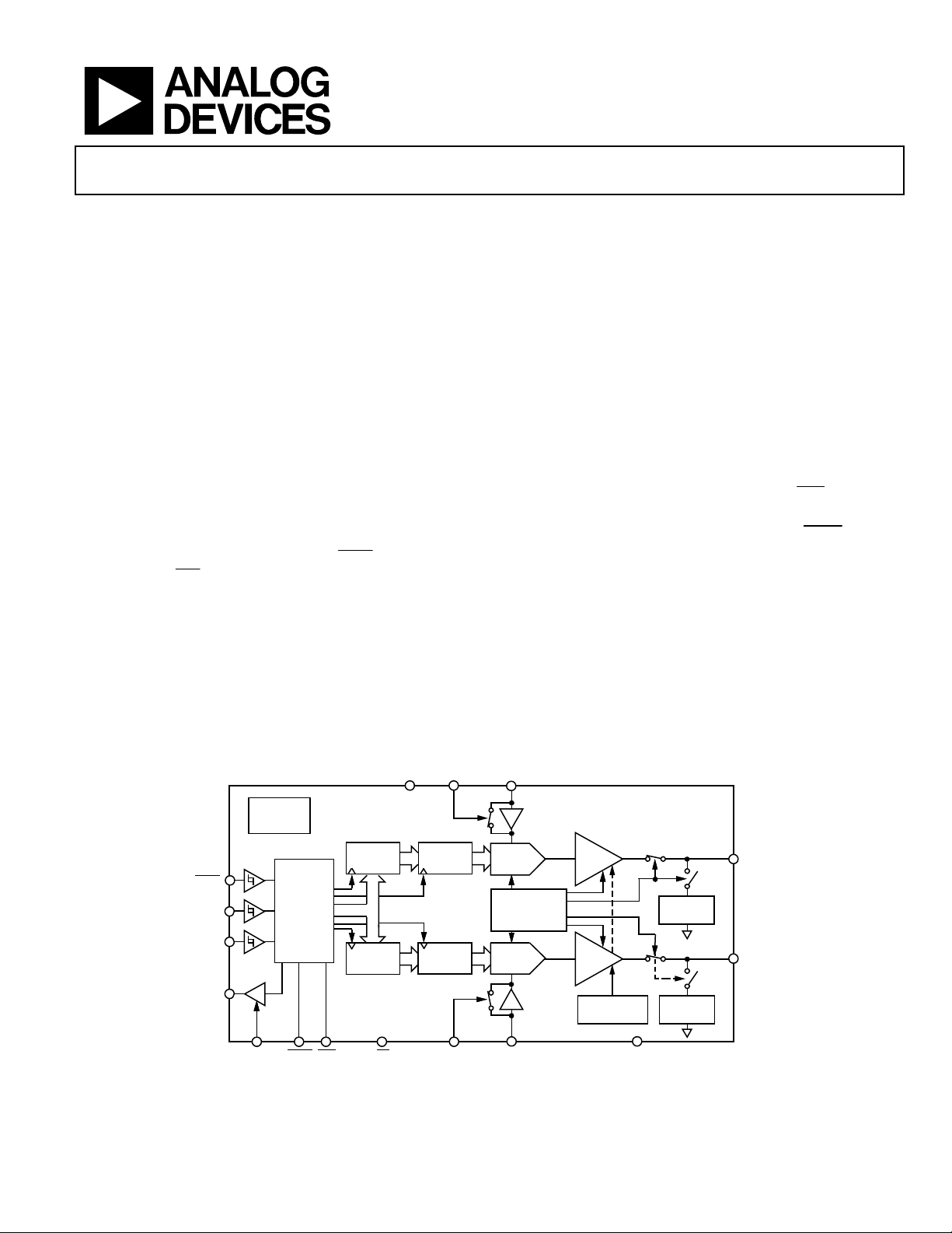
FUNCTIONAL BLOCK DIAGRAM
DD
BUF A
POWER-ON
RESET
INPUT
REGISTER
SYNC
INTERFACE
DCEN
LOGIC
LDAC
INPUT
REGISTER
CLR PD
SCLK
DIN
SDO
Rev. B
Information furnished by Analog Devices is believed to be accurate and reliable. However, no
responsibility is assumed by Analog Devices for its use, nor for any infringements of patents or other
rights of third parties that may result from its use. Specifications subject to change without notice. No
license is granted by implication or otherwise under any patent or patent rights of Analog Devices.
Trademarks and registered trademarks are the property of their respective owners.
DAC
REGISTER
DAC
REGISTER
BUF B
V
A
REF
AD5303/AD5313/AD5323
STRING
DAC
POWER-DOWN
LOGIC
STRING
DAC
B
REF
Figure 1.
One Technology Way, P.O. Box 9106, Norwood, MA 02062-9106, U.S.A.
Tel: 781.329.4700 www.analog.com
Fax: 781.461.3113 ©1999–2007 Analog Devices, Inc. All rights reserved.
BUFFER
BUFFER
GAIN-SELECT
LOGIC
RESISTOR
NETWORK
RESISTOR
NETWORK
GNDV
A
V
OUT
B
V
OUT
00472-001
Page 2

AD5303/AD5313/AD5323
TABLE OF CONTENTS
Features.............................................................................................. 1
Applications....................................................................................... 1
General Description ......................................................................... 1
Functional Block Diagram .............................................................. 1
Revision History ............................................................................... 2
Specifications..................................................................................... 3
AC Characteristics........................................................................ 6
Timing Characteristics ................................................................ 6
Absolute Maximum Ratings............................................................ 8
ESD Caution.................................................................................. 8
Pin Configuration and Function Descriptions............................. 9
Terminology .................................................................................... 10
Typical Performance Characteristics ........................................... 11
Functional Description.................................................................. 15
Digital-to-Analog .......................................................................15
Resistor String............................................................................. 15
DAC Reference Inputs............................................................... 15
Output Amplifier........................................................................ 15
Power-On Reset .............................................................................. 16
Clear Function (
Serial Interface ................................................................................17
CLR
) ................................................................ 16
Input Shift Register .................................................................... 17
Low Power Serial Interface ....................................................... 17
Double-Buffered Interface ........................................................ 17
Power-Down Modes ...................................................................... 19
Microprocesser Interfacing ........................................................... 20
AD5303/AD5313/AD5323 to ADSP-2101 Interface............. 20
AD5303/AD5313/AD5323 to 68HC11/68L11 Interface ...... 20
AD5303/AD5313/AD5323 to 80C51/80L51 Interface.......... 20
AD5303/AD5313/AD5323 to MICROWIRE Interface ........ 20
Applications Information.............................................................. 21
Typical Application Circuit....................................................... 21
Bipolar Operation Using the AD5303/AD5313/AD5323. .... 21
Opto-Isolated Interface for Process Control Applications ... 22
Decoding Multiple AD5303/AD5313/AD5323s.................... 22
AD5303/AD5313/AD5323 as a Digitally Programmable
Window Detector....................................................................... 22
Coarse and Fine Adjustment Using the
AD5303/AD5313/AD5323 ....................................................... 23
Daisy-Chain Mode..................................................................... 23
Power Supply Bypassing and Grounding................................ 24
Outline Dimensions....................................................................... 25
Ordering Guide .......................................................................... 25
REVISION HISTORY
6/07—Rev. A to Rev. B
Updated Format..................................................................Universal
Changes to Table 4............................................................................ 8
Changes to the Ordering Guide.................................................... 25
8/03—Rev. 0 to Rev. A
Added A Version.................................................................Universal
Changes to Features.......................................................................... 1
Changes to Specifications................................................................ 2
Changes to Absolute Maximum Ratings....................................... 5
Changes to Ordering Guide............................................................ 5
Updated Outline Dimensions....................................................... 18
4/99—Revision 0: Initial Version
Rev. B | Page 2 of 28
Page 3

AD5303/AD5313/AD5323
SPECIFICATIONS
VDD = 2.5 V to 5.5 V; V
= 2 V; RL = 2 kΩ to GND; CL = 200 pF to GND; all specifications T
REF
MIN
to T
, unless otherwise noted.
MAX
Table 1.
A Version
Parameter
DC PERFORMANCE
2
3, 4
Min Typ Max Min Typ Max Unit Conditions/Comments
1
B Version
AD5303
Resolution 8 8 Bits
Relative Accuracy ±0.15 ±1 ± 0.15 ±0.5 LSB
Differential Nonlinearity ±0.02 ±0.25 ± 0.02 ±0.25 LSB Guaranteed monotonic by design over
AD5313
Resolution 10 10 Bits
Relative Accuracy ±0.5 ±4 ± 0.5 ±2 LSB
Differential Nonlinearity ±0.05 ±0.5 ± 0.05 ±0.5 LSB Guaranteed monotonic by design over
AD5323
Resolution 12 12 Bits
Relative Accuracy ±2 ±16 ±2 ±8 LSB
Differential Nonlinearity ±0.2 ±1 ±0.2 ±1 LSB Guaranteed monotonic by design over
Offset Error ±0.4 ±3 ±0.4 ±3 % of FSR
Gain Error ±0.15 ±1 ±0.15 ±1 % of FSR
Lower Dead Band 10 60 10 60 mV
Offset Error Drift
Gain Error Drift
Power Supply Rejection Ratio
DC Crosstalk5
DAC REFERENCE INPUTS
Input Range
REF
V
Input Impedance
REF
5
5
−12 −12 ppm of FSR/°C
−5 −5 ppm of FSR/°C
5
−60 −60 dB ΔVDD = ±10%
30 30 μV
5
1 VDD 1 VDD V Buffered reference mode V
0 V
0 VDD V Unbuffered reference mode
DD
>10 >10 MΩ Buffered reference mode
180 180 kΩ Unbuffered reference mode
0 V to V
90 90 kΩ Unbuffered reference mode
0 V to 2 V
Reference Feedthrough −90 −90 dB Frequency = 10 kHz
Channel-to-Channel Isolation −80 −80 dB Frequency = 10 kHz
OUTPUT CHARACTERISTICS
Minimum Output Voltage
Maximum Output Voltage
5
6
0.001 0.001 V min
6
VDD − 0.001 VDD − 0.001 V max
DC Output Impedance 0.5 0.5 Ω
Short-Circuit Current 50 50 mA VDD = 5 V
20 20 mA VDD = 3 V
Power-Up Time 2.5 2.5 μs Coming out of power-down mode;
5 5 μs Coming out of power-down mode;
1
all codes
all codes
all codes
See
Figure 2 and Figure 3
See
Figure 2 and Figure 3
See
Figure 2 and Figure 3
output range, input
REF
impedance = R
impedance = R
DAC
output range, input
REF
DAC
This is a measure of the minimum and
maximum drive capability of the output
amplifier
= 5 V
V
DD
= 3 V
V
DD
Rev. B | Page 3 of 28
Page 4

AD5303/AD5313/AD5323
A Version
Parameter
LOGIC INPUTS
2
5
Min Typ Max Min Typ Max Unit Conditions/Comments
1
B Version
1
Input Current ±1 ±1 μA
Input Low Voltage, VIL
0.8 0.8 V VDD = 5 V ± 10%
0.6 0.6 V VDD = 3 V ± 10%
0.5 0.5 V VDD = 2.5 V
Input High Voltage, VIH
2.4 2.4 V VDD = 5 V ± 10%
2.1 2.1 V VDD = 3 V ± 10%
2.0 2.0 V VDD = 2.5 V
Pin Capacitance 2 3.5 2 3.5 pF
LOGIC OUTPUT (SDO)
5
VDD = 5 V ± 10%
Output Low Voltage 0.4 0.4 V I
Output High Voltage 4.0 4.0 V I
SINK
SOURCE
= 2 mA
= 2 mA
VDD = 3 V ± 10%
Output Low Voltage 0.4 0.4 V I
Output High Voltage 2.4 2.4 V I
= 2 mA
SINK
SOURCE
= 2 mA
Floating-State Leakage Current 1 1 μA DCEN = GND
Floating-State Output
3 3 pF DCEN = GND
Capacitance
POWER REQUIREMENTS
VDD 2.5 5.5 2.5 5.5 V IDD specification is valid for all DAC codes
IDD (Normal Mode) Both DACs active and excluding load
currents
VDD = 4.5 V to 5.5 V 300 450 300 450 μA
VDD = 2.5 V to 3.6 V 230 350 230 350 μA
Both DACs in unbuffered mode;
= VDD and VIL = GND; in buffered
V
IH
mode, extra current is typically x μA
per DAC, where x = 5 μA + V
REF/RDAC
IDD (Full Power-Down)
VDD = 4.5 V to 5.5 V 0.2 1 0.2 1 μA
VDD = 2.5 V to 3.6 V 0.05 1 0.05 1 μA
1
Temperature range for Version A, Version B: −40°C to +105°C.
2
See the Terminology section.
3
DC specifications tested with the outputs unloaded.
4
Linearity is tested using a reduced code range: AD5303 (Code 8 to Code 248); AD5313 (Code 28 to Code 995); AD5323 (Code 115 to Code 3981).
5
Guaranteed by design and characterization, not production tested.
6
In order for the amplifier output to reach its minimum voltage, offset error must be negative. In order for the amplifier output to reach its maximum voltage, V
and offset plus gain error must be positive.
REF
= VDD
Rev. B | Page 4 of 28
Page 5
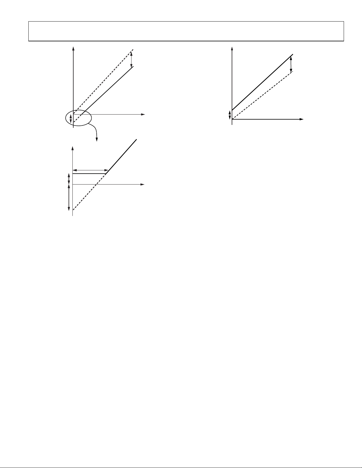
AD5303/AD5313/AD5323
R
V
GAIN ERROR
OUTPUT
VOLTAGE
IDEAL
PLUS
OFFSET ERRO
OUTPUT
OLTAGE
ACTUAL
GAIN ERROR
PLUS
OFFSET ERROR
ACTUAL
POSITIVE
OFFSET
ERROR
AMPLIFIER
FOOTROOM
(1mV)
NEGATIVE
OFFSET
ERROR
DAC CODE
DEAD BAND
Figure 2. Transfer Function with Negative Offset
IDEAL
POSITIVE
OFFSET
ERROR
Figure 3. Transfer Function with Positive Offset
DAC CODE
00472-006
0472-005
Rev. B | Page 5 of 28
Page 6
AD5303/AD5313/AD5323
AC CHARACTERISTICS
VDD = 2.5 V to 5.5 V; RL = 2 kΩ to GND; CL = 200 pF to GND; all specifications T
1
MIN
to T
, unless otherwise noted.
MAX
Table 2.
A, B Version
Parameter
2
Min Typ Max
Output Voltage Settling Time V
3
Unit Conditions/Comments
= VDD = 5 V
REF
AD5303 6 8 μs ¼ scale to ¾ scale change (0x40 to 0xc0)
AD5313 7 9 μs ¼ scale to ¾ scale change (0x100 to 0x300)
AD5323 8 10 μs ¼ scale to ¾ scale change (0x400 to 0xc00)
Slew Rate 0.7 V/μs
Major-Code Transition Glitch Energy 12 nV-s 1 LSB change around major carry
(011 . . . 11 to 100 . . . 00)
Digital Feedthrough 0.10 nV-s
Analog Crosstalk 0.01 nV-s
DAC-to-DAC Crosstalk 0.01 nV-s
Multiplying Bandwidth 200 kHz V
Total Harmonic Distortion −70 dB V
1
Guaranteed by design and characterization, not production tested.
2
See the Terminology section.
3
Temperature range for Version A and Version B: −40°C to +105°C.
= 2 V ± 0.1 V p-p, unbuffered mode
REF
= 2.5 V ± 0.1 V p-p, frequency = 10 kHz
REF
TIMING CHARACTERISTICS
VDD = 2.5 V to 5.5 V; all specifications T
MIN
to T
, unless otherwise noted.
MAX
Table 3.
Parameter
1, 2, 3
Limit at T
(A, B Version)
MIN, TMAX
Unit Conditions/Comments
t1 33 ns min SCLK cycle time
t2 13 ns min SCLK high time
t3 13 ns min SCLK low time
t4 0 ns min
SYNC to SCLK rising edge setup time
t5 5 ns min Data setup time
t6 4.5 ns min Data hold time
t7 0 ns min
t8 100 ns min
t9 20 ns min
t10 20 ns min
t11 20 ns min
4, 5
t
12
4, 5
t
20 ns max SCLK falling edge to SDO valid
13
5
t
14
5
t
15
1
Guaranteed by design and characterization, not production tested.
2
All input signals are specified with tr = tf = 5 ns (10% to 90% of VDD) and timed from a voltage level of (VIL + VIH)/2.
3
See Figure 4 and Figure 5.
4
These are measured with the load circuit of Figure 4.
5
Daisy-chain mode only (see Figure 47).
5 ns min SCLK falling edge to SDO invalid
0 ns min
10 ns min
SCLK falling edge to
Minimum
SYNC high time
LDAC pulse width
SCLK falling edge to
CLR pulse width
SCLK falling edge to
SYNC rising edge to SCLK rising edge
SYNC rising edge
LDAC rising edge
SYNC rising edge
Rev. B | Page 6 of 28
Page 7
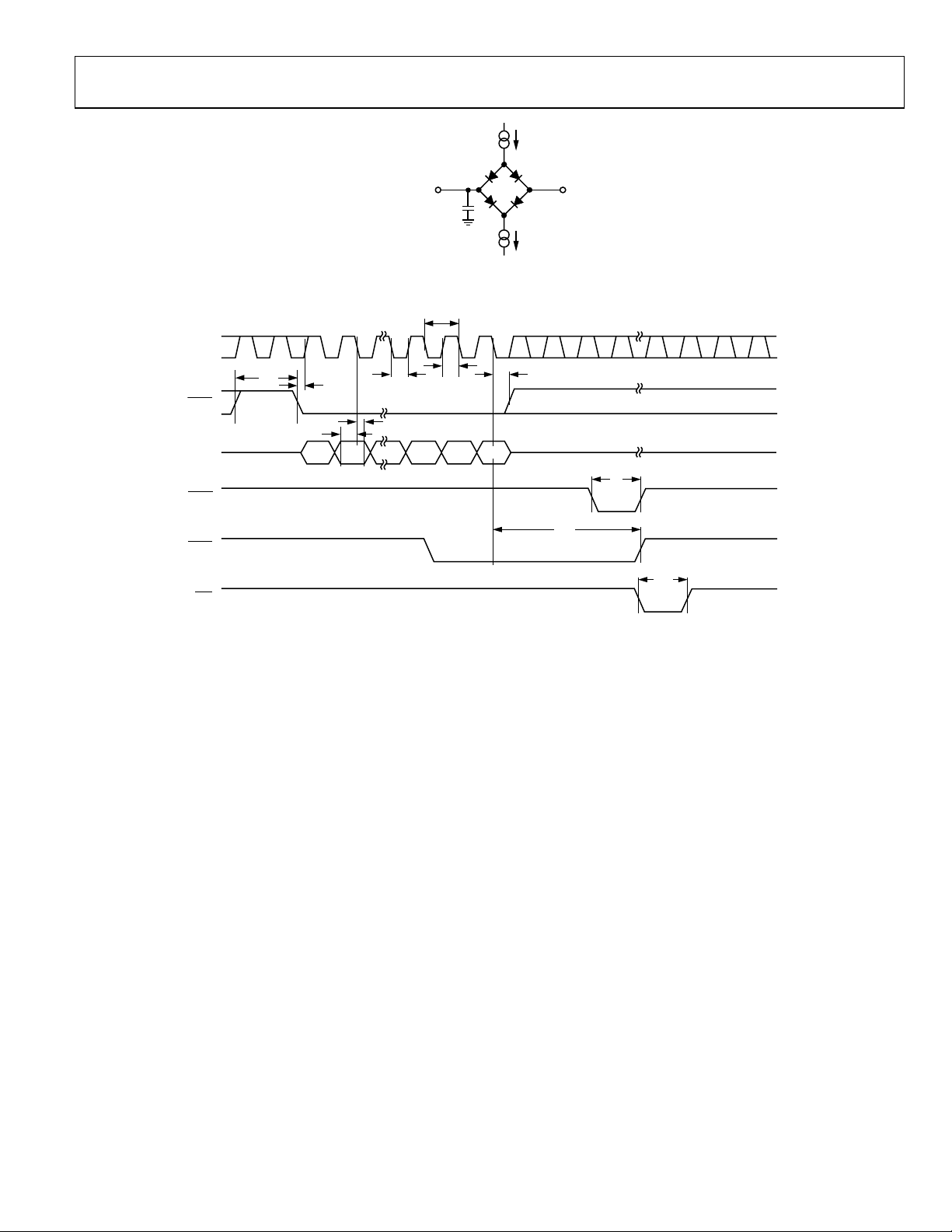
AD5303/AD5313/AD5323
S
2mA I
OL
TO OUTPUT
PIN
50pF
C
L
2mA I
1.6V
OH
00472-002
Figure 4. Load Circuit for Digital Output (SDO) Timing Specifications
t
1
SCLK
t
t
8
YNC
DIN* DB15
LDAC
LDAC
CLR
*
SEE THE INPUT SHIFT REGISTER SECTION.
t
4
t
6
t
5
t
3
Figure 5. Serial Interface Timing Diagram
2
DB0
t
7
t
9
t
10
t
11
00472-003
Rev. B | Page 7 of 28
Page 8
AD5303/AD5313/AD5323
ABSOLUTE MAXIMUM RATINGS
TA = 25°C, unless otherwise noted.1
Table 4.
Parameter Rating
VDD to GND −0.3 V to +7 V
Digital Input Voltage to GND −0.3 V to VDD + 0.3 V
Digital Output Voltage to GND −0.3 V to VDD + 0.3 V
Reference Input Voltage to GND −0.3 V to VDD + 0.3 V
V
A, V
OUT
Operating Temperature Range
Industrial (A, B Version) −40°C to +105°C
Storage Temperature Range −65°C to +150°C
Junction Temperature (TJ Max) 150°C
16-Lead TSSOP Package
Power Dissipation (TJ max − TA)/θJA
θJA Thermal Impedance 160°C/W
Lead Temperature JEDEC Industry Standard
1
Transient currents of up to 100 mA do not cause SCR latch-up.
B to GND −0.3 V to VDD + 0.3 V
OUT
Soldering J-STD-020
Stresses above those listed under Absolute Maximum Ratings
may cause permanent damage to the device. This is a stress
rating only; functional operation of the device at these or any
other conditions above those indicated in the operational
section of this specification is not implied. Exposure to absolute
maximum rating conditions for extended periods may affect
device reliability.
ESD CAUTION
Rev. B | Page 8 of 28
Page 9
AD5303/AD5313/AD5323
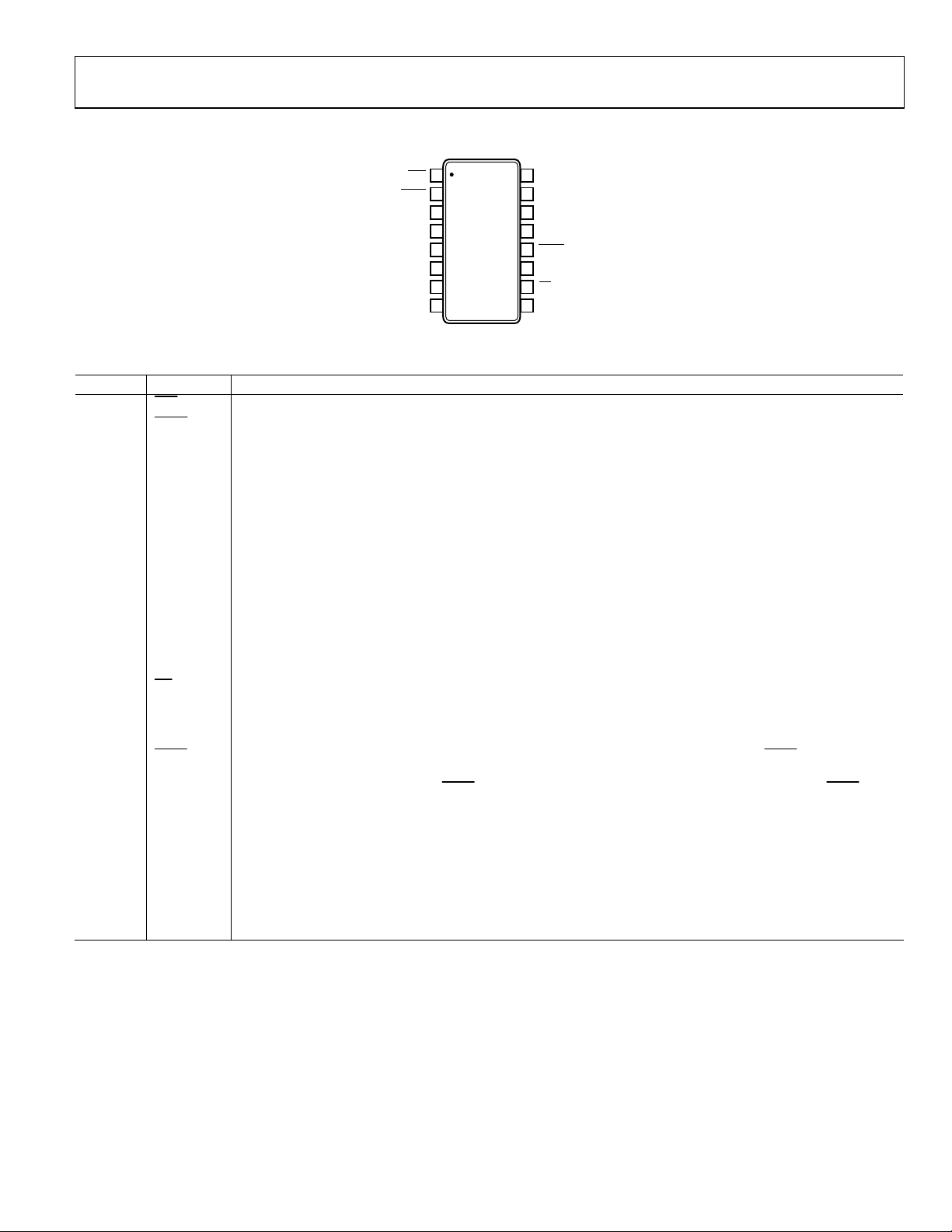
V
PIN CONFIGURATION AND FUNCTION DESCRIPTIONS
CLR
LDAC
V
V
REF
V
REF
OUT
BUF A
BUF B
DD
B
A
A
1
2
AD5303/
3
AD5313/
4
AD5323
5
TOP VIEW
(Not to Scale)
6
7
8
16
SDO
15
GND
14
DIN
13
SCLK
12
SYNC
11
B
V
OUT
10
PD
9
DCEN
00472-004
Figure 6. Pin Configuration
Table 5. Pin Function Descriptions
Pin No. Mnemonic Description
1
2
CLR
LDAC Active Low Control Input. Transfers the contents of the input registers to their respective DAC registers. Pulsing
Active Low Control Input. Loads all zeros to both input and DAC registers.
this pin low allows either or both DAC registers to be updated if the input registers have new data. This allows
the simultaneous update of both DAC outputs.
3 VDD Power Supply Input. These parts can be operated from 2.5 V to 5.5 V, and the supply should be decoupled to GND.
4 V
5 V
6 V
7 BUF A
B
REF
A
REF
A Buffered Analog Output Voltage from DAC A. The output amplifier has rail-to-rail operation.
OUT
Reference Input Pin for DAC B. It may be configured as a buffered or an unbuffered input, depending on the state
of the BUF B pin. It has an input range from 0 V to V
in unbuffered mode and from 1 V to VDD in buffered mode.
DD
Reference Input Pin for DAC A. It may be configured as a buffered or an unbuffered input depending on the state
of the BUF A pin. It has an input range from 0 to V
in unbuffered mode and from 1 V to VDD in buffered mode.
DD
Control Pin. Controls whether the reference input for DAC A is unbuffered or buffered. If this pin is tied low, the
reference input is unbuffered. If it is tied high, the reference input is buffered.
8 BUF B
Control Pin. Controls whether the reference input for DAC B is unbuffered or buffered. If this pin is tied low, the
reference input is unbuffered. If it is tied high, the reference input is buffered.
9 DCEN
This pin is used to enable the daisy-chaining option. This should be tied high if the part is being used in a daisy
chain. The pin should be tied low if it is being used in standalone mode.
10
PD Active Low Control Input. Acts as a hardware power-down option. This pin overrides any software power-down
option. Both DACs go into power-down mode when this pin is tied low. The DAC outputs go into a high
impedance state and the current consumption of the part drops to 200 nA @ 5 V (50 nA @ 3 V).
11 V
12
B Buffered Analog Output Voltage from DAC B. The output amplifier has rail-to-rail operation.
OUT
SYNC Active Low Control Input. This is the frame synchronization signal for the input data. When SYNC goes low, it
powers on the SCLK and DIN buffers and enables the input shift register. Data is transferred in on the falling
edges of the following 16 clocks. If
SYNC is taken high before the 16th falling edge, the rising edge of SYNC acts
as an interrupt and the write sequence is ignored by the device.
13 SCLK
Serial Clock Input. Data is clocked into the input shift register on the falling edge of the serial clock input. Data
can be transferred at rates up to 30 MHz. The SCLK input buffer is powered down after each write cycle.
14 DIN
Serial Data Input. This device has a 16-bit shift register. Data is clocked into the register on the falling edge of the
serial clock input. The DIN input buffer is powered down after each write cycle.
15 GND Ground Reference Point for All Circuitry on the Part.
16 SDO
Serial Data Output. Can be used for daisy-chaining a number of these devices together or for reading back the
data in the shift register for diagnostic purposes. The serial data output is valid on the falling edge of the clock.
Rev. B | Page 9 of 28
Page 10

AD5303/AD5313/AD5323
TERMINOLOGY
Relative Accuracy or Integral Nonlinearity (INL)
For the DAC, relative accuracy or integral nonlinearity is a
measure of the maximum deviation, in LSB, from a straight
line passing through the actual endpoints of the DAC transfer
function. A typical INL error vs. code plot can be seen in
Figure 7, Figure 8, and Figure 9.
Differential Nonlinearity (DNL)
Differential nonlinearity is the difference between the measured
change and the ideal 1 LSB change between any two adjacent
codes. A specified DNL of ±1 LSB maximum ensures monotonicity. This DAC is guaranteed monotonic by design. A typical
DNL error vs. code plot can be seen in
Figure 10, Figure 11, and
Figure 12.
Offset Error
This is a measure of the offset error of the DAC and the output
amplifier. It is expressed as a percentage of the full-scale range.
Gain Error
This is a measure of the span error of the DAC. It is the deviation in slope of the actual DAC transfer characteristic from the
ideal expressed as a percentage of the full-scale range.
Offset Error Drift
This is a measure of the change in offset error with changes in
temperature. It is expressed in (ppm of full-scale range)/°C.
Gain Error Drift
This is a measure of the change in gain error with changes in
temperature. It is expressed in (ppm of full-scale range)/°C.
Major-Code Transition Glitch Energy
Major-code transition glitch energy is the energy of the impulse
injected into the analog output when the code in the DAC register
changes state. It is normally specified as the area of the glitch in
nV-s and is measured when the digital code is changed by 1 LSB
at the major carry transition (011 . . . 11 to 100 . . . 00 or 100 . . .
00 to 011 . . . 11).
Digital Feedthrough
Digital feedthrough is a measure of the impulse injected into
the analog output of the DAC from the digital input pins of the
device, but is measured when the DAC is not being written to
SYNC
(
held high). It is specified in nV-s and is measured with a
full-scale change on the digital input pins, that is, from all 0s to
all 1s and vice versa.
Analog Crosstalk
This is the glitch impulse transferred to the output of one DAC
due to a change in the output of the other DAC. It is measured
by loading one of the input registers with a full-scale code
change (all 0s to all 1s and vice versa) while keeping
high. Then pulse
LDAC
low and monitor the output of the
LDAC
DAC whose digital code was not changed. The area of the
glitch is expressed in nV-s.
DAC-to-DAC Crosstalk
This is the glitch impulse transferred to the output of one DAC
due to a digital code change and subsequent output change of
the other DAC. This includes both digital and analog crosstalk.
It is measured by loading one of the DACs with a full-scale code
change (all 0s to all 1s and vice versa) while keeping
LDAC
low
and monitoring the output of the other DAC. The area of the
glitch is expressed in nV-s.
DC Crosstalk
This is the dc change in the output level of one DAC in response
to a change in the output of the other DAC. It is measured with
a full-scale output change on one DAC while monitoring the
other DAC. It is expressed in microvolts.
Power Supply Rejection Ratio (PSRR)
This indicates how the output of the DAC is affected by changes
in the supply voltage. PSRR is the ratio of the change in V
a change in V
in decibels. V
for full-scale output of the DAC. It is measured
DD
is held at 2 V and VDD is varied ±10%.
REF
OUT
to
Reference Feedthrough
This is the ratio of the amplitude of the signal at the DAC output to
the reference input when the DAC output is not being updated
(that is,
LDAC
is high). It is expressed in decibels.
Total Harmonic Distortion (THD)
This is the difference between an ideal sine wave and its
attenuated version using the DAC. The sine wave is used as
the reference for the DAC and the THD is a measure of the
harmonics present on the DAC output. It is measured in
decibels.
Multiplying Bandwidth
The amplifiers within the DAC have a finite bandwidth. The
multiplying bandwidth is a measure of this. A sine wave on the
reference (with full-scale code loaded to the DAC) appears on
the output. The multiplying bandwidth is the frequency at
which the output amplitude falls to 3 dB below the input.
Channel-To-Channel Isolation
This is a ratio of the amplitude of the signal at the output of one
DAC to a sine wave on the reference input of the other DAC. It
is measured in decibels.
Rev. B | Page 10 of 28
Page 11

AD5303/AD5313/AD5323
TYPICAL PERFORMANCE CHARACTERISTICS
1.0
0.5
TA = 25°C
V
= 5V
DD
0.3
0.2
0.1
TA = 25
= 5V
V
DD
°C
0
INL ERROR (L SB)
–0.5
–1.0
0 50 100 150 200 250
CODE
Figure 7. AD5303 Typical INL Plot
3
TA = 25°C
= 5V
V
DD
2
1
0
INL ERROR (LSB)
–1
–2
–3
0 200 400 600 800 1000
CODE
Figure 8. AD5313 Typical INL Plot
12
TA = 25°C
= 5V
V
DD
8
4
0
–0.1
DNL ERROR (LSB)
–0.2
–0.3
00472-007
0 50 100 150 250
CODE
200
00472-010
Figure 10. AD5303 Typical DNL Plot
0.6
TA = 25°C
= 5V
V
DD
0.4
0.2
0
–0.2
DNL ERROR (LSB)
–0.4
–0.6
00472-008
0 200 400 600 800 1000
CODE
00472-011
Figure 11. AD5313 Typical DNL Plot
1.0
TA = 25°C
V
= 5V
DD
0.5
0
INL ERRO R (LS B)
–4
–8
–12
0 1000 2000 3000 4000
CODE
Figure 9. AD5323 Typical INL Plot
00472-009
Rev. B | Page 11 of 28
0
DNL ERROR (LSB)
–0.5
–1.0
0 1000 2000 3000 4000
CODE
Figure 12. AD5323 Typical DNL Plot
00472-012
Page 12

AD5303/AD5313/AD5323
1.00
0.75
0.50
TA = 25
V
= 5V
DD
°C
VDD = 3V
VDD = 5V
ERROR (LSB)
ERROR (LSB)
0.25
–0.25
–0.50
–0.75
–1.00
1.00
0.75
0.50
0.25
–0.25
–0.50
–0.75
–1.00
MAX INL
0
2345
VDD = 5V
V
REF
0
–40
MAX DNL
MIN DNL
MIN INL
V
(V)
REF
Figure 13. AD5303 INL and DNL Error vs. V
= 3V
MAX DNL
MIN INL
04080120
TEMPERATURE ( °C)
MAX INL
MIN DNL
REF
00472-013
Figure 14. AD5303 INL Error and DNL Error vs. Temperature
1.0
VDD = 5V
=2V
V
REF
0.5
GAIN ERROR
0
ERROR (%)
–0.5
OFFSET ERROR
FREQUENCY
0
100 150 200 250 300 350 400
IDD (µA)
00472-016
Figure 16. IDD Histogram with VDD = 3 V and VDD = 5 V
5
5V SOURCE
4
3
(V)
OUT
V
2
1
–0
00472-014
0123456
SINK/SOURCE CURRENT (mA)
5V SINK
3V SOURCE
3V SINK
00472-017
Figure 17. Source and Sink Current Capability
600
TA = 25°C
V
= 5V
DD
500
400
(µA)
300
DD
I
200
100
–1.0
–40
0 40 80 120
TEMPERATURE ( °C)
Figure 15. Offset Error and Gain Error vs. Temperature
00472-015
Rev. B | Page 12 of 28
0
ZERO SCALE FULL SCALE
Figure 18. Supply Current vs. Code
00472-018
Page 13

AD5303/AD5313/AD5323
C
C
600
BOTH DACS IN G AIN-OF-T WO MODE
REFERENCE INPUT S BUFFERED
500
400
(µA)
300
DD
I
200
100
0
2.5 3.0 3.5 4.0 4.5 5.0 5.5
+25°C
–40°C
+105°C
V
(V)
DD
Figure 19. Supply Current vs. Supply Voltage
1.0
BOTH DACS IN
0.9
THREE-STATE CONDITION
0.8
0.7
0.6
0.5
(µA)
DD
I
0.4
0.3
0.2
0.1
0
2.7 3.2 3.7 4.2 4.7 5.2
–40°C
+25°C
+105°C
VDD (V)
Figure 20. Power-Down Current vs. Supply Voltage
700
TA = 25°C
600
CLK
H2
H1
00472-019
V
OUT
CH1 1V, CH2 5V, T IME BASE = 5µ s/DIV
Figure 22. Half-Scale Settling (¼ to ¾ Scale Code Change)
TA = 25°C
V
DD
CH1
CH2
CH1 1V, CH2 1V, TI ME BASE = 20µs/DIV
00472-020
V
Figure 23. Power-On Reset to 0 V
TA = 25°C
OUT
A
VDD = 5V
T
= 25°C
A
00472-022
00472-023
500
400
(µA)
DD
I
300
200
100
0 0.5 1.0 1.5 2.0 2.5 3.0 3.5 4.0 4.5 5.0
VDD = 3V
V
LOGIC
VDD = 5V
(V)
Figure 21. Supply Current vs. Logic Input Voltage
CH1
CH3
00472-021
Figure 24. Exiting Power-Down to Midscale
V
OUT
CLK
CH1 1V, CH3 5V, TI ME BASE = 1µs /DIV
00472-024
Rev. B | Page 13 of 28
Page 14

AD5303/AD5313/AD5323
V
2.50
2.49
(V)
OUT
V
2.48
2mV/DI
2.47
1µs/DIV
Figure 25. AD5323 Major-Code Transition
10
0
–10
–20
(dB)
–30
–40
–50
–60
10 100 1k 10k 100k 1M 10M
FREQUENCY(Hz)
Figure 26. Multiplying Bandwidth (Small-Signal Frequency Response)
00472-025
500ns/DIV
00472-027
Figure 27. DAC-to-DAC Crosstalk
0.10
TA = 25°C
V
= 5V
DD
0.05
0
FULL-SCAL E ERROR (V)
–0.05
–0.10
012345
00472-026
Figure 28. Full-Scale Error vs. V
V
REF
(V)
(Buffered)
REF
00472-028
Rev. B | Page 14 of 28
Page 15

AD5303/AD5313/AD5323
V
V
A
FUNCTIONAL DESCRIPTION
The AD5303/AD5313/AD5323 are dual resistor-string DACs
fabricated on a CMOS process with resolutions of 8-/10-/12-bits
respectively. They contain reference buffers and output buffer
amplifiers, and are written to via a 3-wire serial interface. They
operate from single supplies of 2.5 V to 5.5 V and the output
buffer amplifiers provide rail-to-rail output swing with a slew
rate of 0.7 V/μs. Each DAC is provided with a separate reference
input, which may be buffered to draw virtually no current from
the reference source, or unbuffered to give a reference input
range from GND to V
. The devices have three programmable
DD
power-down modes, in which one or both DACs may be turned
off completely with a high impedance output, or the output may
be pulled low by an on-chip resistor.
DIGITAL-TO-ANALOG
The architecture of one DAC channel consists of a reference
buffer and a resistor-string DAC followed by an output buffer
amplifier. The voltage at the V
voltage for the DAC.
Figure 29 shows a block diagram of the
DAC architecture. Because the input coding to the DAC is
straight binary, the ideal output voltage is given by
×
D
V
OUT
REF
=
N
2
where:
D is the decimal equivalent of the binary code, which is loaded
to the DAC register:
0 to 255 for AD5303 (8 bits)
0 to 1023 for AD5313 (10 bits)
0 to 4095 for AD5323 (12 bits)
N is the DAC resolution.
REFERENCE
INPUT
REGISTER
DAC
REGISTER
Figure 29. Single DAC Channel Architecture
pin provides the reference
REF
REF
BUFFER
RESISTOR
STRING
OUTPUT BUFF ER
SWITCH
CONTROLL ED
BY CONTROL
LOGIC
AMPLI FIER
V
A
OUT
00472-029
RESISTOR STRING
The resistor string section of the AD5303/AD5313/AD5323
is shown in
Figure 30. It is simply a string of resistors, each of
value R. The digital code loaded to the DAC register determines
at what node on the string the voltage is tapped off to be fed
into the output amplifier. The voltage is tapped off by closing
one of the switches connecting the string to the amplifier.
Because it is a string of resistors, it is guaranteed monotonic.
R
R
R
R
R
Figure 30. Resistor String
TO OUTP UT
AMPLIFIER
00472-030
DAC REFERENCE INPUTS
There is a reference input pin for each of the two DACs. The
reference inputs are buffered, but can also be configured as
unbuffered. The advantage with the buffered input is the high
impedance it presents to the voltage source driving it. However,
if the unbuffered mode is used, the user can have a reference
voltage as low as GND and as high as V
since there is no
DD
restriction due to headroom and footroom of the reference
amplifier.
If there is a buffered reference in the circuit (for example,
REF192), there is no need to use the on-chip buffers of the
AD5303/AD5313/AD5323. In unbuffered mode, the input
impedance is still large at typically 180 kΩ per reference input
for 0 V to V
mode and 90 kΩ for 0 V to 2 V
REF
mode.
REF
The buffered/unbuffered option is controlled by the BUF A
and BUF B pins. If a BUF pin is tied high, the reference input
is buffered; if tied low, it is unbuffered.
OUTPUT AMPLIFIER
The output buffer amplifier is capable of generating output
voltages to within 1 mV of either rail, which gives an output
range of 0.001 V to V
It is capable of driving a load of 2 kΩ in parallel with 500 pF to
GND and V
. The source and sink capabilities of the output
DD
amplifier can be seen in
The slew rate is 0.7 V/μs with a half-scale settling time to
±0.5 LSB (at eight bits) of 6 μs.
− 0.001 V when the reference is VDD.
DD
Figure 17.
Rev. B | Page 15 of 28
Page 16

AD5303/AD5313/AD5323
POWER-ON RESET
The AD5303/AD5313/AD5323 are provided with a power-on
reset function, so that they power up in a defined state. The
power-on state is with 0V to V
set to 0 V.
Both input and DAC registers are filled with zeros and remain
so until a valid write sequence is made to the device. This is
output range and the output
REF
particularly useful in applications where it is important to know
the state of the DAC outputs while the device is powering up.
CLEAR FUNCTION (CLR)
CLR
The
all zeros to both input registers and both DAC registers. This
enables both analog outputs to be cleared to 0 V.
pin is an active low input that, when pulled low, loads
Rev. B | Page 16 of 28
Page 17

AD5303/AD5313/AD5323
SERIAL INTERFACE
The AD5303/AD5313/AD5323 are controlled over a versatile,
3-wire serial interface, which operates at clock rates up to
30 MHz and is compatible with SPI, QSPI, MICROWIRE,
and DSP interface standards.
INPUT SHIFT REGISTER
The input shift register is 16 bits wide. Data is loaded into
the device as a 16-bit word under the control of a serial clock
input, SCLK. The timing diagram for this operation is shown in
Figure 5. The 16-bit word consists of four control bits followed
by 8 /10 /12 bits of DAC data, depending on the device type.
The first bit loaded is the MSB (Bit 15), which determines whether
the data is for DAC A or DAC B. Bit 14 determines the output
range (0 V to V
operating mode of the DAC.
Table 6. Control Bits
Bit Name Function
15
A/B 0: data written to DAC A
14 GAIN
13 PD1 Mode bit 0
12 PD0 Mode bit 0
The remaining bits are DAC data bits, starting with the MSB
and ending with the LSB. The AD5323 uses all 12 bits of DAC
data; the AD5313 uses 10 bits and ignores the 2 LSBs. The
AD5303 uses eight bits and ignores the last four bits. The data
format is straight binary, with all 0s corresponding to 0 V output,
and all 1s corresponding to full-scale output (V
SYNC
The
synchronization signal and chip enable. Data can be transferred
into the device only while
transfer,
SYNC
SYNC
to SCLK rising edge setup time, t4. After
serial data is shifted into the device’s input shift register on the
falling edges of SCLK for 16 clock pulses. Any data and clock
pulses after the 16th are ignored, and no further serial data
transfer occurs until
SYNC
may be taken high after the falling edge of the 16th SCLK
pulse, observing the minimum SCLK falling edge to
rising edge time, t
or 0 V to 2 V
REF
1: data written to DAC B
0: output range of 0 V to V
1: output range of 0 V to 2 V
). Bit 13 and Bit 12 control the
REF
Power-On
Default
N/A
0
REF
REF
− 1 LSB).
REF
input is a level-triggered input that acts as a frame
SYNC
is low. To start the serial data
should be taken low, observing the minimum
SYNC
goes low,
SYNC
is taken high and low again.
SYNC
.
7
After the end of serial data transfer, data is automatically
transferred from the input shift register to the input register
of the selected DAC. If
SYNC
is taken high before the 16th
falling edge of SCLK, the data transfer is aborted and the input
registers are not updated.
When data has been transferred into both input registers, the
DAC registers of both DACs may be simultaneously updated,
by taking
LDAC
low.
CLR
is an active low, asynchronous clear
that clears the input and DAC registers of both DACs to all 0s.
LOW POWER SERIAL INTERFACE
To reduce the power consumption of the device even further,
the interface only powers up fully when the device is being
written to. As soon as the 16-bit control word has been written
to the part, the SCLK and DIN input buffers are powered down.
They only power up again following a falling edge of
SYNC
.
DOUBLE-BUFFERED INTERFACE
The DACs all have double-buffered interfaces consisting of two
banks of registers—input registers and DAC registers. The input
register is connected directly to the input shift register and the
digital code is transferred to the relevant input register on completion of a valid write sequence. The DAC register contains the
digital code used by the resistor string.
LDAC
Access to the DAC register is controlled by the
LDAC
When
is high, the DAC register is latched and the input
register may change state without affecting the contents of the
DAC register. However, when
LDAC
is brought low, the DAC
register becomes transparent and the contents of the input register are transferred to it.
This is useful if the user requires simultaneous updating of
both DAC outputs. The user may write to both input registers
individually and then, by pulsing the
LDAC
input low, both
outputs update simultaneously.
These parts contain an extra feature whereby the DAC register
is not updated unless its input register has been updated since
the last time that
LDAC
was brought low. Normally, when
is brought low, the DAC registers are filled with the contents of
the input registers. In the case of the AD5303/AD5313/AD5323,
the part only updates the DAC register if the input register has
been changed since the last time the DAC register was updated,
thereby removing unnecessary digital crosstalk.
function.
LDAC
Rev. B | Page 17 of 28
Page 18

AD5303/AD5313/AD5323
DB15 (MSB) DB0 (LSB)
A/B
PD0 D7 D6 D5 D4 D3 D2 D1 D0PD1GAIN X X X X
DATA BITS
00472-031
Figure 31. AD5303 Input Shift Register Contents
DB15 (MSB) DB0 (LSB)
A/B
PD0 D7D6D5D4 D3D2 D1D0PD1GAIN XX
D9 D8
DATA BITS
0472-032
Figure 32. AD5313 Input Shift Register Contents
DB15 (MSB) DB0 (LSB)
A/B
PD0 D7D6D5D4D3D2D1D0PD1GAIN
D9 D8D11 D10
DATA BITS
00472-033
Figure 33. AD5323 Input Shift Register Contents
Rev. B | Page 18 of 28
Page 19

AD5303/AD5313/AD5323
A
R
POWER-DOWN MODES
The AD5303/AD5313/AD5323 have very low power consumption, dissipating only 0.7 mW with a 3 V supply and 1.5 mW
with a 5 V supply. Power consumption can be further reduced
when the DACs are not in use by putting them into one of three
power-down modes, which are selected by Bit 13 and Bit 12
(PD1 and PD0) of the control word.
Table 7 shows how the
state of the bits corresponds to the mode of operation of that
particular DAC.
Table 7. PD1/PD0 Operating Modes
PD1 PD0 Operating Mode
0 0 Normal operation
0 1 Power-down (1 kΩ load to GND)
1 0 Power-down (100 kΩ load to GND)
1 1 Power-down (high impedance output)
When both bits are set to 0, the DACs work normally with their
normal power consumption of 300 μA at 5 V. However, for the
three power-down modes, the supply current falls to 200 nA at
5 V (50 nA at 3 V) when both DACs are powered down. Not
only does the supply current drop, but the output stage is also
internally switched from the output of the amplifier to a resistor
network of known values. This has the advantage that the
output impedance of the part is known while the part is in
power-down mode and provides a defined input condition
for whatever is connected to the output of the DAC amplifier.
There are three different power-down options. The output is
connected internally to GND through either a 1 kΩ resistor or
a 100 kΩ resistor, or it is left in a high impedance state (threestate). The output stage is illustrated in
Figure 34.
The bias generator, the output amplifier, the resistor string, and
all other associated linear circuitry are shut down when the
power-down mode is activated. However, the contents of the
registers are unaffected when in power-down. The time to exit
power-down is typically 2.5 μs for V
V
= 3 V (see Figure 24 for a plot).
DD
= 5 V and 5 μs when
DD
The software power-down modes programmed by PD0 and
PD1 are overridden by the
PD
pin. Taking this pin low puts
both DACs into power-down mode simultaneously and both
outputs are put into a high impedance state. If
PD
is not used,
it should be tied high.
MPLIFIE
RESISTOR
STRING DAC
POWER-DOWN
CIRCUITRY
Figure 34. Output Stage During Power-Down
RESISTOR
NETWORK
V
OUT
00472-034
Rev. B | Page 19 of 28
Page 20

AD5303/AD5313/AD5323
*
*
MICROPROCESSER INTERFACING
AD5303/AD5313/AD5323 TO ADSP-2101 INTERFACE
Figure 35 shows a serial interface between the AD5303/AD5313/
AD5323 and the
ADSP-2101. The ADSP-2101 should be set up
to operate in the SPORT transmit alternate framing mode. The
ADSP-2101 sport is programmed through the SPORT control
register and should be configured as follows: internal clock
operation, active-low framing, 16-bit word length. Transmission
is initiated by writing a word to the Tx register after the SPORT
has been enabled.
ADSP-2101
TFS
DT
SCLK
ADDITIONAL PINS OMIT TED FOR CL ARITY
Figure 35. AD5303/AD5313/AD5323 to ADSP-2101 Interface
AD5303/
AD5313/
AD5323*
SYNC
DIN
SCLK
00472-035
AD5303/AD5313/AD5323 TO 68HC11/68L11 INTERFACE
Figure 36 shows a serial interface between the AD5303/
AD5313/AD5323 and the 68HC11/68L11 microcontroller.
SCK of the 68HC11/68L11 drives the SCLK of the AD5303/
AD5313/AD5323, while the MOSI output drives the serial data
line (DIN) of the DAC. The
line (PC7). The setup conditions for correct operation of this
interface are as follows: the 68HC11/68L11 should be configured so that its CPOL bit is a 0 and its CPHA bit is a 1.
When data is being transmitted to the DAC, the
is taken low (PC7). When the 68HC11/68L11 is configured
as previously mentioned, data appearing on the MOSI output
is valid on the falling edge of SCK. Serial data from the 68HC11/
68L11 is transmitted in 8-bit bytes with only eight falling clock
edges occurring in the transmit cycle. Data is transmitted MSB
first. To load data to the AD5303/AD5313/ AD5323, PC7 is left
low after the first eight bits are transferred and a second serial
write operation is performed to the DAC; PC7 is taken high at
the end of this procedure.
68HC11/68L11*
PC7
SCK
MOSI
*ADDITIONA L PINS OMI TTED FOR CLARITY
Figure 36. AD5303/AD5313/AD5323 to 68HC11/68L11 Interface
SYNC
signal is derived from a port
SYNC
AD5303/
AD5313/
AD5323*
SYNC
SCLK
DIN
line
6
3
0
2
7
4
0
0
AD5303/AD5313/AD5323 TO 80C51/80L51 INTERFACE
Figure 37 shows a serial interface between the AD5303/
AD5313/AD5323 and the 80C51/80L51 microcontroller. The
setup for the interface is as follows: TXD of the 80C51/80L51
drives SCLK of the AD5303/AD5313/AD5323, while RXD
drives the serial data line of the part. The
SYNC
signal is again
derived from a bit programmable pin on the port. In this case,
port line P3.3 is used. When data is to be transmitted to the
AD5303/AD5313/AD5323, P3.3 is taken low. The 80C51/80L51
transmits data only in 8-bit bytes; thus only eight falling clock
edges occur in the transmit cycle. To load data to the DAC, P3.3
is left low after the first eight bits are transmitted and a second
write cycle is initiated to transmit the second byte of data. P3.3
is taken high following the completion of this cycle. The 80C51/
80L51 output the serial data in a format that has the LSB first.
The AD5303/AD5313/AD5323 require data with MSB as the
first bit received. The 80C51/80L51 transmit routine should
take this into account.
80C51/80L51*
P3.3
TXD
RXD
*ADDITIONA L PINS OMI TTED FO R CLARITY.
Figure 37. AD5303/AD5313/AD5323 to 80C51/80L51 Interface
AD5303/
AD5313/
AD5323*
SYNC
SCLK
DIN
00472-037
AD5303/AD5313/AD5323 TO MICROWIRE INTERFACE
Figure 38 shows an interface between the AD5303/AD5313/
AD5323 and any MICROWIRE-compatible device. Serial
data is shifted out on the falling edge of the serial clock and
is clocked into the AD5303/AD5313/AD5323 on the rising
edge of the SK.
MICROWIRE*
CS SYNC
SO
ADDITIONAL PINS OM ITTED F OR CLARIT Y.
Figure 38. AD5303/AD5313/AD5323 to MICROWIRE Interface
AD5303/
AD5313/
AD5323*
SCLKSK
DIN
00472-038
Rev. B | Page 20 of 28
Page 21

AD5303/AD5313/AD5323
V
V
V
V
[
APPLICATIONS INFORMATION
TYPICAL APPLICATION CIRCUIT
The AD5303/AD5313/AD5323 can be used with a wide range
of reference voltages, especially if the reference inputs are configured to be unbuffered, in which case the devices offer a full,
one-quadrant multiplying capability over a reference range of
0 V to V
More typically, the AD5303/AD5313/AD5323 may be used
with a fixed precision reference voltage.
typical setup for the AD5303/AD5313/AD5323 when using
an external reference. If the reference inputs are unbuffered,
the reference input range is from 0 V to V
reference buffers are used, the reference range is reduced. Suitable references for 5 V operation are the
(2.5 V references). For 2.5 V operation, a suitable external
reference is the
If an output range of 0 V to VDD is required when the reference
inputs are configured as unbuffered (for example, 0 V to 5 V),
the simplest solution is to connect the reference inputs to V
As this supply may not be very accurate and may be noisy, the
AD5303/AD5313/AD5323 can be powered from the reference
voltage, for example, using a 5 V reference such as the
as shown in
voltage for the AD5303/AD5313/AD5323. The supply current
required from the
or 60 μA into each of the reference inputs (if unbuffered). This
is with no load on the DAC outputs. When the DAC outputs are
loaded, the
loads. The total current required (with a 10 kΩ load on each
output) is
The load regulation of the
results in an error of 2.7 ppm (13.5 μV) for the 1.36 mA current
drawn from it. This corresponds to a 0.0007 LSB error at eight
bits and 0.011 LSB error at 12 bits.
.
DD
Figure 39 shows a
, but if the on-chip
DD
AD780 and REF192
REF191, a 2.048 V reference.
= 2.5V to 5.5
DD
V
EXT
V
OUT
REF
AD780/REF192
WITH V
= 5V
DD
OR REF191 WI TH
V
= 2.5V
DD
1µF
SERIAL
INTERFACE
V
V
AD5303/AD5313/
SYNC
REF
REF
SCLK
DIN
GND
DD
A
B
AD5323
BUF A BUF B
V
A
OUT
V
B
OUT
Figure 39. AD5303/AD5313/AD5323 Using External Reference
Figure 40. The REF195 outputs a steady supply
REF195 is 300 μA and approximately 30 μA
REF195 also needs to supply the current to the
360 μA + 2(5 V/10 kΩ) = 1.36 mA
REF195 is typically 2 ppm/mA, which
00472-039
DD
REF195,
.
15
V
S
REF195
OUTPUT
GND
0.1µF 10µ F
1µF
V
DD
V
A
REF
V
B
REF
A
V
OUT
AD5303/AD5313/
AD5323
SCLK
SERIAL
INTERFACE
DIN
SYNC
GND BUF A BUF B
B
V
OUT
00472-040
Figure 40. Using an REF195 as Power and Reference to the
AD5303/AD5313/AD5323
BIPOLAR OPERATION USING THE AD5303/ AD5313/AD5323
The AD5303/AD5313/AD5323 have been designed for singlesupply operation, but bipolar operation is also achievable using
the circuit shown in
figured to achieve an output voltage range of −5 V < V
Rail-to-rail operation at the amplifier output is achievable using
an
AD820 or OP295 as the output amplifier.
6V to 16
V
S
REF195
OUTPUT
GND
Figure 41. Bipolar Operation Using the AD5303/AD5313/AD5323
The output voltage for any input code can be calculated as
follows:
OUT
REF
where:
D is the decimal equivalent of the code loaded to the DAC.
N is the DAC resolution.
V
is the reference voltage input, and gain bit = 0, with
REF
V
= 5 V
REF
R1 = R2 = 10 kΩ and V
OUT
Figure 41. The circuit shown has been con-
R2
0.1µF 10µF
1µF
SERIAL
INTERFACE
VDD = 5V
V
DD
V
A/B
REF
AD5303/AD5313/
AD5323
SCLK
DIN
SYNC
GND BUF A BUF B
N
= 5 V,
DD
N
VDV
5)2/10( −×=
10kΩ
V
R1
OUT
A/B
10kΩ
REF
+5V
–5V
×−+××=
< +5 V.
OUT
AD820/
OP295
±5V
)/(/)()2/()( R1R2VR1R2R1DVV
]
00472-041
Rev. B | Page 21 of 28
Page 22

AD5303/AD5313/AD5323
SYNC
K
V
OPTO-ISOLATED INTERFACE FOR PROCESS CONTROL APPLICATIONS
The AD5303/AD5313/AD5323 has a versatile 3-wire serial
interface making it ideal for generating accurate voltages in
process control and industrial applications. Due to noise, safety
requirements, or distance, it may be necessary to isolate the
AD5303/AD5313/AD5323 from the controller. This can easily
be achieved by using opto-isolators, which provides isolation
in excess of 3 kV. The serial loading structure of the AD5303/
AD5313/AD5323 makes it ideally suited for use in opto-isolated
applications.
AD5303/AD5313/AD5323 where DIN, SCLK, and
Figure 42 shows an opto-isolated interface to the
SYNC
are
driven from opto-couplers. The power supply to the part also
needs to be isolated. This is done by using a transformer. On the
DAC side of the transformer, a 5 V regulator provides the 5 V
supply required for the AD5303/AD5313/AD5323.
5V
POWER
SCL
DIN
REGULATOR
V
DD
10kΩ
V
DD
10kΩ
V
DD
10kΩ
SCLK
AD5303/AD5313/
AD5323
SYNC
DIN
GND BUF A BUF B
Figure 42. AD5303/AD5313/AD5323 in an Opto-Isolated Interface
V
DD
10µF 0.1µF
V
A
REF
V
B
REF
V
A
OUT
V
B
OUT
00472-042
DECODING MULTIPLE AD5303/AD5313/AD5323s
SYNC
The
in applications to decode a number of DACs. In this application,
all the DACs in the system receive the same serial clock and
serial data, but only the
any one time, allowing access to two channels in this 8-channel
system. The 74HC139 is used as a 2-to-4 line decoder to address
any of the DACs in the system. To prevent timing errors from
occurring, the enable input should be brought to its inactive
state while the coded address inputs are changing state.
Figure 43 shows a diagram of a typical setup for decoding
multiple AD5303/AD5313/AD5323 devices in a system.
pin on the AD5303/AD5313/AD5323 can be used
SYNC
to one of the devices is active at
SCLK
DIN
ENABLE
CODED
ADDRESS
1G
1A
1B
V
DD
V
CC
74HC139
DGND
1Y0
1Y1
1Y2
1Y3
SYNC
DIN
SCLK
SYNC
DIN
SCLK
AD5303/
AD5313/
AD5323
AD5303/
AD5313/
AD5323
AD5303/
SYNC
AD5313/
DIN
AD5323
SCLK
AD5303/
AD5313/
SYNC
DIN
AD5323
SCLK
Figure 43. Decoding Multiple AD5303/AD5313/AD5323 Devices in a System
AD5303/AD5313/AD5323 AS A DIGITALLY PROGRAMMABLE WINDOW DETECTOR
A digitally programmable upper/lower limit detector using
the two DACs in the AD5303/AD5313/AD5323 is shown in
Figure 44. The upper and lower limits for the test are loaded
to DAC A and DAC B, which, in turn, set the limits on the
CMP04. If the signal at the VIN input is not within the pro-
grammed window, an LED indicates the fail condition.
5
0.1µF 10µF
V
REF
V
A
REF
V
B
REF
AD5303/AD5313/
AD5323
SYNC
DIN
SCLK
SYNC
DIN
SCLK
GND
Figure 44. Window Detector Using AD5303/AD5313/AD5323
V
IN
V
DD
A
V
OUT
CMP04
V
B
OUT
1/2
1kΩ 1kΩ
FAIL PASS
PAS S/FA IL
1/6 74HC05
00472-043
00472-044
Rev. B | Page 22 of 28
Page 23

AD5303/AD5313/AD5323
V
V
W
COARSE AND FINE ADJUSTMENT USING THE AD5303/AD5313/AD5323
The DACs in the AD5303/AD5313/AD5323 can be paired
together to form a coarse and fine adjustment function, as
shown in
Figure 45. DAC A provides the coarse adjustment
while DAC B provides the fine adjustment. Varying the ratio
of R1 and R2 changes the relative effect of the coarse and fine
adjustments. With the resistor values and external reference
shown, the output amplifier has unity gain for the DAC A
output, so the output range is 0 V to 2.5 V − 1 LSB. For
DAC B, the amplifier has a gain of 7.6 × 10
–3
, giving DAC B
a range equal to 19 mV.
The circuit is shown with a 2.5 V reference, but reference
voltages up to V
may be used. The op amps indicated allow
DD
a rail-to-rail output swing.
= 5
V
IN
EXT 2.5V
REF
V
OUT
GND
AD780/REF192
ITH VDD = 5V
0.1µF
1µF
10µF
V
REF
DD
V
A
R3
51.2kΩ
DD
V
A
OUT
390Ω
AD5303/AD5313/
AD5323
V
B
V
REF
GND
OUT
B
51.2kΩ
Figure 45. Coarse and Fine Adjustment
R4
900Ω
+5V
V
R1
R2
AD820/
OP295
OUT
DAISY-CHAIN MODE
This mode is used for updating serially connected or standalone
SYNC
devices on the rising edge of
several DACs, or where the user wishes to read back the DAC
contents for diagnostic purposes, the SDO pin may be used to
daisy-chain several devices together and provide serial readback.
By connecting the daisy-chain enable (DCEN) pin high, the
daisy-chain mode is enabled. It is tied low in standalone mode.
In daisy-chain mode, the internal gating on SCLK is disabled.
The SCLK is continuously applied to the input shift register
SYNC
when
is low. If more than 16 clock pulses are applied,
the data ripples out of the shift register and appears on the SDO
line. This data is clocked out after the falling edge of SCLK and
is valid on the subsequent rising and falling edges. By connecting this line to the DIN input on the next DAC in the chain, a
multiDAC interface is constructed. Sixteen clock pulses are
required for each DAC in the system. Therefore, the total
number of clock cycles must equal 16N, where N is the total
number of devices in the chain. When the serial transfer to all
devices is complete,
SYNC
should be taken high. This prevents
any further data from being clocked into the input shift register.
. For systems that contain
00472-045
A continuous SCLK source may be used if it can be arranged
SYNC
that
is held low for the correct number of clock cycles.
Alternatively, a burst clock containing the exact number of
clock cycles may be used and
SYNC
may be taken high some
time later.
When the transfer to all input registers is complete, a common
LDAC
signal updates all DAC registers and all analog outputs
are updated simultaneously.
DIN
SCLK
SYNC
LDAC
SCLK
SYNC
LDAC
SCLK
SYNC
LDAC
AD5303/
AD5313/
AD5323
(DAC 1)
SDO
DIN
AD5303/
AD5313/
AD5323
(DAC 2)
SDO
DIN
AD5303/
AD5313/
AD5323
(DAC N)
SDO
1
1
1
00472-046
1
68HC11
MOSI
SCK
PC7
PC6
MISO
1
ADDITIONAL PI NS OMITT ED FOR CLARITY.
Figure 46. Daisy-Chain Mode
Rev. B | Page 23 of 28
Page 24

AD5303/AD5313/AD5323
SCLK
t
8
SYNC
DIN
SDO
t
4
t
6
t
5
DB15 DB0 DB15 DB0
INPUT WORD FOR DAC N INPUT WORD FO R DAC (N+1)
UNDEFINED INPUT WORD FOR DAC N
SCLK
SDO
t
1
t
3
Figure 47. Daisy-Chaining Timing Diagram
POWER SUPPLY BYPASSING AND GROUNDING
In any circuit where accuracy is important, careful consideration of the power supply and ground return layout helps to
ensure the rated performance. The printed circuit board on
which the AD5303/AD5313/AD5323 are mounted should be
designed so that the analog and digital sections are separated
and confined to certain areas of the board. If the AD5303/
AD5313/AD5323 are in a system where multiple devices
require an AGND-to-DGND connection, the connection
should be made at one point only. The star ground point
should be established as close as possible to the AD5303/
AD5313/AD5323. The AD5303/AD5313/AD5323 should
have ample supply bypassing of 10 μF in parallel with 0.1 μF
on the supply located as close to the package as possible, ideally
right up against the device. Use 10 μF capacitors that are of the
tantalum bead type. The 0.1 μF capacitor should have low
effective series resistance (ESR) and effective series inductance
t
2
DB15 DB0
t
13
V
V
t
12
IH
IL
t
14
t
15
00472-047
(ESI), like the common ceramic types that provide a low
impedance path to ground at high frequencies to handle
transient currents due to internal logic switching.
The power supply lines of the AD5303/AD5313/AD5323 should
use as large a trace as possible to provide low impedance paths
and reduce the effects of glitches on the power supply line. Fast
switching signals such as clocks should be shielded with digital
ground to avoid radiating noise to other parts of the board, and
should never be run near the reference inputs. Avoid crossover
of digital and analog signals. Traces on opposite sides of the
board should run at right angles to each other. This reduces
the effects of feedthrough through the board. A microstrip
technique is by far the best, but is not always possible with a
double-sided board. In this technique, the component side of
the board is dedicated to the ground plane while signal traces
are placed on the solder side.
Rev. B | Page 24 of 28
Page 25

AD5303/AD5313/AD5323
OUTLINE DIMENSIONS
5.10
5.00
4.90
0.15
0.05
4.50
4.40
4.30
PIN 1
16
0.65
BSC
COPLANARITY
COMPLIANT TO JEDEC STANDARDS MO-153-AB
0.10
0.30
0.19
9
81
1.20
MAX
SEATING
PLANE
6.40
BSC
0.20
0.09
8°
0°
0.75
0.60
0.45
Figure 48. 16-Lead Thin Shrink Small Outline Package [TSSOP]
(RU-16)
Dimensions shown in millimeters
ORDERING GUIDE
Model Temperature Range Package Description Package Option
AD5303ARU –40°C to +105°C 16-Lead Thin Shrink Small Outline Package (TSSOP) RU-16
AD5303ARU-REEL7 –40°C to +105°C 16-Lead Thin Shrink Small Outline Package (TSSOP) RU-16
AD5303ARUZ
AD5303BRU –40°C to +105°C 16-Lead Thin Shrink Small Outline Package (TSSOP) RU-16
AD5303BRU-REEL –40°C to +105°C 16-Lead Thin Shrink Small Outline Package (TSSOP) RU-16
AD5303BRU-REEL7 –40°C to +105°C 16-Lead Thin Shrink Small Outline Package (TSSOP) RU-16
AD5303BRUZ
AD5303BRUZ-REEL7
AD5313ARU –40°C to +105°C 16-Lead Thin Shrink Small Outline Package (TSSOP) RU-16
AD5313ARU-REEL7 –40°C to +105°C 16-Lead Thin Shrink Small Outline Package (TSSOP) RU-16
AD5313ARUZ
AD5313BRU –40°C to +105°C 16-Lead Thin Shrink Small Outline Package (TSSOP) RU-16
AD5313BRU-REEL –40°C to +105°C 16-Lead Thin Shrink Small Outline Package (TSSOP) RU-16
AD5313BRU-REEL7 –40°C to +105°C 16-Lead Thin Shrink Small Outline Package (TSSOP) RU-16
AD5313BRUZ
AD5323ARU –40°C to +105°C 16-Lead Thin Shrink Small Outline Package (TSSOP) RU-16
AD5323ARU-REEL7 –40°C to +105°C 16-Lead Thin Shrink Small Outline Package (TSSOP) RU-16
AD5323ARUZ
AD5323ARUZ-REEL7
AD5323BRU –40°C to +105°C 16-Lead Thin Shrink Small Outline Package (TSSOP) RU-16
AD5323BRU-REEL –40°C to +105°C 16-Lead Thin Shrink Small Outline Package (TSSOP) RU-16
AD5323BRU-REEL7 –40°C to +105°C 16-Lead Thin Shrink Small Outline Package (TSSOP) RU-16
AD5323BRUZ
AD5323BRUZ-REEL
AD5323BRUZ-REEL7
1
Z = RoHS Compliant Part.
1
1
1
1
1
1
1
1
1
1
–40°C to +105°C 16-Lead Thin Shrink Small Outline Package (TSSOP) RU-16
–40°C to +105°C 16-Lead Thin Shrink Small Outline Package (TSSOP) RU-16
–40°C to +105°C 16-Lead Thin Shrink Small Outline Package (TSSOP) RU-16
–40°C to +105°C 16-Lead Thin Shrink Small Outline Package (TSSOP) RU-16
–40°C to +105°C 16-Lead Thin Shrink Small Outline Package (TSSOP) RU-16
–40°C to +105°C 16-Lead Thin Shrink Small Outline Package (TSSOP) RU-16
–40°C to +105°C 16-Lead Thin Shrink Small Outline Package (TSSOP) RU-16
–40°C to +105°C 16-Lead Thin Shrink Small Outline Package (TSSOP) RU-16
–40°C to +105°C 16-Lead Thin Shrink Small Outline Package (TSSOP) RU-16
–40°C to +105°C 16-Lead Thin Shrink Small Outline Package (TSSOP) RU-16
Rev. B | Page 25 of 28
Page 26

AD5303/AD5313/AD5323
NOTES
Rev. B | Page 26 of 28
Page 27

AD5303/AD5313/AD5323
NOTES
Rev. B | Page 27 of 28
Page 28

AD5303/AD5313/AD5323
NOTES
©1999–2007 Analog Devices, Inc. All rights reserved. Trademarks and
registered trademarks are the property of their respective owners.
C00472-0-6/07(B)
Rev. B | Page 28 of 28
 Loading...