

Page 1
64-Position OTP Digital Potentiometer
FEATURES
64 positions
One-time-programmable (OTP)
Resistance setting—low cost alternative over EEMEM
Unlimited adjustments prior to OTP activation
1 kΩ, 10 kΩ, 50 kΩ, 100 kΩ end-to-end terminal resistance
Compact SOT-23-8 standard package
Ultralow power: I
Fast settling time: t
2
C®-compatible digital interface
I
Computer software
= 5 µA maximum
DD
= 5 µs typ during power-up
S
2
replaces µC in
factory programming applications
Wide temperature range: −40°C to +105°C
Low operating voltage: 2.7 V to 5.5 V
OTP validation check function
APPLICATIONS
System calibrations
Electronics level settings
Mechanical potentiometers and trimmer replacement
Automotive electronics adjustments
Transducer circuit adjustments
Programmable filters up to 6 MHz BW
GENERAL DESCRIPTION
The AD5273 is a 64-position, one-time-programmable (OTP)
digital potentiometer
achieve permanent program setting. This device performs the
same electronic adjustment function as most mechanical
trimmers and variable resistors. It allows unlimited adjustments
before permanently setting the resistance values. The AD5273 is
programmed using a 2-wire, I
During write mode, a fuse blow command is executed after the
final value is determined, thereby freezing the wiper position at
a given setting (analogous to placing epoxy on a mechanical
trimmer). When permanent setting is achieved, the value will
not change, regardless of the supply variations or environmental
stresses under normal operating conditions. To verify the success
of permanent programming, Analog Devices patterned the OTP
validation such that the fuse status can be discerned from two
validation bits in the read mode.
4
that employs fuse link technology to
1
set-and-forget
3
2
C-compatible digital control.
AD5273
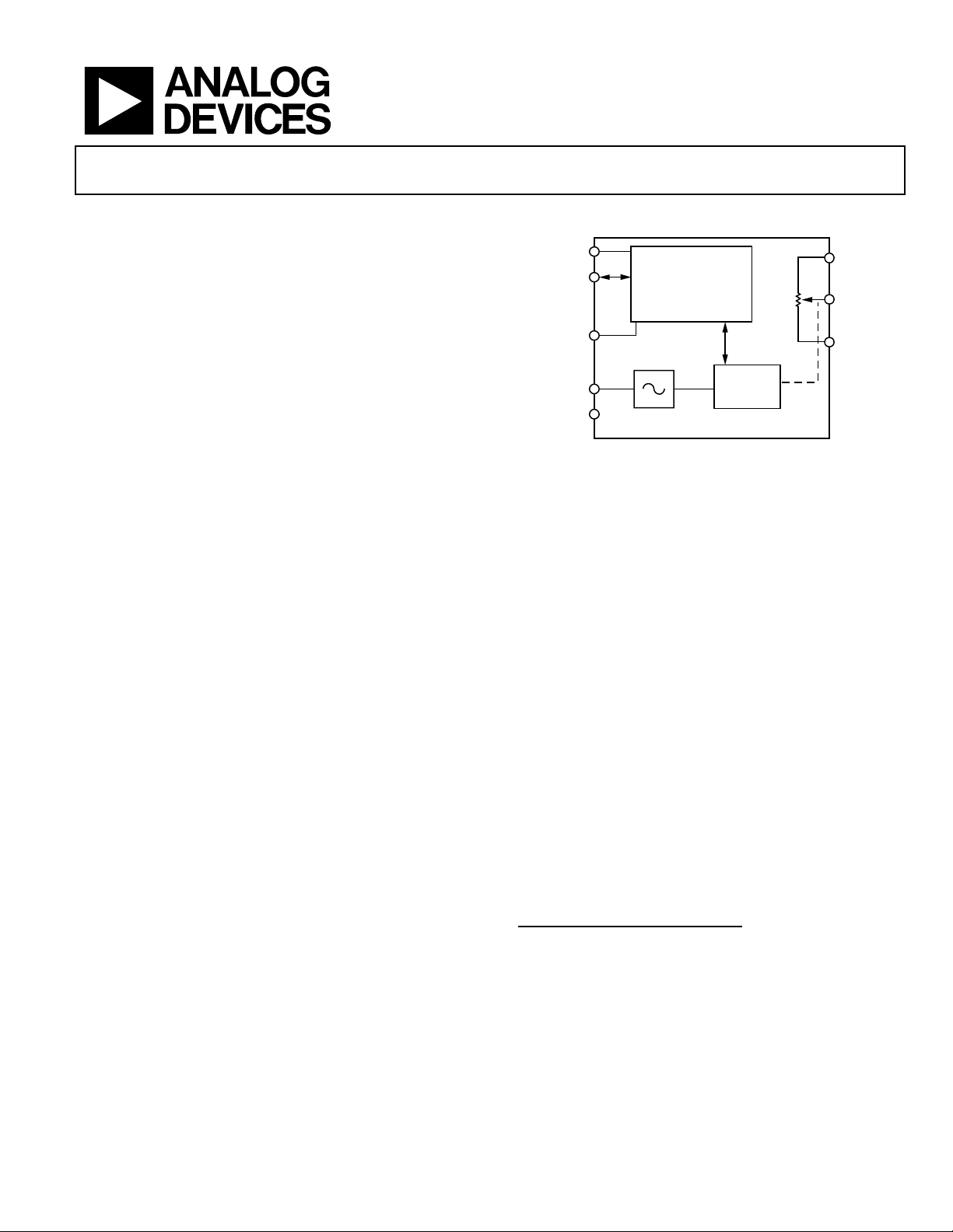
FUNCTIONAL BLOCK DIAGRAM
SCL
SDA
AD0
V
GND
DD
I2C INTERFACE
AND
CONTROL LOGIC
AD5273
FUSE
LINK
Figure 1.
WIPER
REGISTER
In addition, for applications that program the AD5273 at the
factory, Analog Devices offers device programming software
running on Windows
® NT, Windows 2000, and Windows XP
operating systems. This software application effectively replaces
any external I
2
C controllers, which in turn enhances the user
system’s time-to-market.
The AD5273 is available in 1 kΩ, 10 kΩ, 50 kΩ, and 100 kΩ
resistances and in a compact SOT-23 8-lead standard package.
It operates from −40°C to +105°C.
Along with its unique OTP feature, the AD5273 lends itself
well to general digital potentiometer applications due to its
effective resolution, array resistance options, small footprint,
and low cost.
An AD5273 evaluation kit and software are available. The kit
includes the connector and cable that can be converted for
factory programming applications.
For applications that require dynamic adjustment of resistance
settings with nonvolatile EEMEM, users should refer to the
AD523x and AD525x families of nonvolatile memory digital
potentiometers.
1
OTP allows unlimited adjustments before permanent setting.
2
ADI cannot guarantee the software to be 100% compatible to all systems
due to the wide variation in computer configurations.
3
Applies to 1 kΩ parts only.
4
The terms digital potentiometer, VR, and RDAC are used interchangeably.
A
W
B
03224-001
2
Rev. E
Information furnished by Analog Devices is believed to be accurate and reliable.
However, no responsibility is assumed by Analog Devices for its use, nor for any
infringements of patents or other rights of third parties that may result from its use.
Specifications subject to change without notice. No license is granted by implication
or otherwise under any patent or patent rights of Analog Devices. Trademarks and
registered trademarks are the property of their respective owners.
One Technology Way, P.O. Box 9106, Norwood, MA 02062-9106, U.S.A.
Tel: 781.329.4700
Fax: 781.326.8703 © 2005 Analog Devices, Inc. All rights reserved.
www.analog.com
Page 2

AD5273
TABLE OF CONTENTS
Specifications..................................................................................... 3
2
I
C Controller Programming.................................................... 17
Absolute Maximum Ratings............................................................ 5
Pin Configuration and Function Descriptions............................. 6
Typical Performance Characteristics ............................................. 7
Theory of Operation ...................................................................... 12
One-Time Programming........................................................... 12
Variable Resistance and Voltage for Rheostat Mode ............. 13
Variable Resistance and Voltage for Potentiometer Mode.... 14
ESD Protection ........................................................................... 14
Terminal Voltage Operating Range.......................................... 14
Power-Up/Power-Down Sequences ......................................... 14
Power Supply Considerations ................................................... 15
Controlling the AD5273................................................................ 16
Software Programming.............................................................. 16
REVISION HISTORY
1/05—Rev. D to Rev. E
Changes to Features.......................................................................... 1
Changes to Specifications................................................................ 3
Changes to Table 3............................................................................ 6
Changes to Power Supply Consideration Section ...................... 15
Changes to Figure 35 and Figure 37............................................. 15
Changes to DAC Section ............................................................... 19
Changes to Level Shift for Different Voltages
Operation Section..................................................................... 20
Deleted the Resistance Scaling Section........................................ 20
Deleted the Resolution Enhancement Section ........................... 20
12/04—Rev. C to Rev. D
Updated Format..................................................................Universal
Changes to Specifications................................................................ 3
Changes to Theory of Operation Section.................................... 13
Changes to Power Supply Consideration Section ...................... 15
Changes to Figure 35, Figure 36, and Figure 37 ......................... 15
11/03—Rev. B to Rev. C
Changes to SDA BIT DEFINITIONS
AND DESCRIPTIONS .................................................................. 10
Changes to ONE-TIME PROGRAMMING (OTP) section..... 11
Changes to Table III .......................................................................11
Changes to POWER SUPPLY CONSIDERATIONS ................. 13
Changes to Figures 8, 9, and 10 .................................................... 13
Controlling Two Devices on One Bus..................................... 18
Applications..................................................................................... 19
DAC.............................................................................................. 19
Programmable Voltage Source with Boosted Output ........... 19
Programmable Current Source ................................................ 19
Gain Control Compensation.................................................... 19
Programmable Low-Pass Filter ................................................ 20
Level Shift for Different Voltages ............................................. 20
RDAC Circuit Simulation Model............................................. 20
Evaluation Board ............................................................................ 21
Outline Dimensions ....................................................................... 22
Ordering Guide .......................................................................... 22
10/03—Rev. A to Rev. B
Changes to FEATURES ....................................................................1
Changes to APPLICATIONS...........................................................1
Changes to SPECIFICATIONS .......................................................2
Changes to ABSOLUTE MAXIMUM RATINGS.........................4
Changes to PIN FUNCTION DESCRIPTIONS...........................5
Changes to TPCs 7, 8, 13, and 14 captions ....................................7
Deleted TPC 20; renumbered successive TPCs.............................9
Change to TPC 21 caption ...............................................................9
Change to the SDA BIT DEFINITIONS
AND DESCRIPTIONS.................................................................. 10
Replaced THEORY OF OPERATION section........................... 11
Replaced DETERMINING THE VARIABLE RESISTANCE
AND VOLTAGE section ............................................................... 11
Replaced ESD PROTECTION section ........................................ 12
Replaced TERMINAL VOLTAGE OPERATING
RANGE section .............................................................................. 12
Replaced POWER-UP SEQUENCE section............................... 12
Replaced POWER SUPPLY CONSIDERATIONS section ....... 13
Changes to APPLICATIONS section .......................................... 16
Change to Equation 9..................................................................... 17
Deleted Digital Potentiometer Family Selection Guide ............ 19
6/03—Rev. 0 to Rev. A
Change to SPECIFICATIONS.........................................................2
Change to POWER SUPPLY CONSIDERATIONS section..... 12
Updated OUTLINE DIMENSIONS ............................................ 20
Rev. E | Page 2 of 24
Page 3

AD5273
SPECIFICATIONS
VDD = 2.7 V to 5.5 V, VA < VDD, VB = 0 V, −40°C < TA < +105°C, unless otherwise noted.
Table 1. Electrical Characteristics 1 kΩ, 10 kΩ, 50 kΩ, 100 kΩ Versions
Parameter Symbol Conditions Min
DC CHARACTERISTICS
RHEOSTAT MODE
Resolution N
Resistor Differential Nonlinearity
2
10 kΩ, 50 kΩ, 100 kΩ
1 kΩ
Resistor Nonlinearity2 R-INL
10 kΩ, 50 kΩ, 100 kΩ
1 kΩ
Nominal Resistance Tolerance
3
10 kΩ, 50 kΩ, 100 kΩ
Nominal Resistance, 1 kΩ R
Rheostat Mode Temperature Coefficient4 (∆RAB/RAB)/∆T Wiper = NC
Wiper Resistance R
DC CHARACTERISTICS
POTENTIOMETER DIVIDER MODE
Differential Nonlinearity
5
Integral Nonlinearity5
Voltage Divider4
Temperature Coefficient (∆VW/VW)/ ∆T Code = 0x20 10 ppm/°C
Full-Scale Error V
10 kΩ, 50 kΩ, 100 kΩ −1 0 LSB
1 kΩ −6 0 LSB
Zero-Scale Error V
10 kΩ, 50 kΩ, 100 kΩ 0 1 LSB
1 kΩ 0 5 LSB
RESISTOR TERMINALS
Voltage Range
6
Capacitance7 A, B CA, C
Capacitance7 W
Common-Mode Leakage I
DIGITAL INPUTS AND OUTPUTS
Input Logic High (SDA and SCL)
8
Input Logic Low (SDA and SCL)8
Input Logic High (ADO) V
Input Logic Low (ADO) V
Input Logic Current I
Input Capacitance7 C
Output Logic Low (SDA) V
Three-State Leakage Current I
Output Capacitance7
POWER SUPPLIES
Power Supply Range V
OTP Power Supply
8, 9
Supply Current I
OTP Supply Current
Power Dissipation
8, 10
11
Power Supply Sensitivity PSRR RAB = 1 kΩ −0.3 +0.3 %/%
PSRR RAB = 10 kΩ, 50 kΩ, 100 kΩ −0.05 +0.05 %/%
R-DNL
RWB, VA = NC −0.5 +0.05 +0.5 LSB
RWB, VA = NC −1 +0.25 +1 LSB
∆RAB/R
AB
AB
RWB, VA = NC −0.5 +0.10 +0.5 LSB
RWB, VA = NC −5 +2 +5 LSB
TA = 25°C
−30
0.8 1.2 1.6 kΩ
W
IW = VDD/R, VDD = 3 V or 5 V
DNL −0.5 +0.1 +0.5 LSB
INL −0.5 +0.5 LSB
Code = 0x3F −1 0 LSB
WFSE
Code = 0x00 −6 0 LSB
WZSE
VA,VB, V
B
C
W
CM
V
IH
V
IL
IH
IL
IL
IL
OL
OZ
C
OZ
DD
V
DD_OTP
DD
I
DD_OTP
P
DISS
W
GND V
f = 5 MHz, measured to GND, code = 0x20 25 pF
f = 1 MHz, measured to GND, code = 0x20 55 pF
VA = VB = V
W
0.7 V
1 nA
DD
−0.5 0.3 V
3.0 V
VIN = 0 V or 5 V 0 0.4 V
0.01 1 µA
3 pF
0.4 V
±1 µA
3 pF
2.7 5.5 V
TA = 25°C 5.25 5.5 V
VIH = 5 V or VIL = 0 VIL = 0 V 0.1 5 µA
TA = 25°C, V
= 5.5 V 100 mA
DD_OTP
VIH = 5 V or VIL = 0 V, VIL = 0 V, VDD = 5 V 0.2 0.03 mW
1
Typ
Max Unit
6 Bits
LSB
300
+30 %
ppm/°C
60 100 Ω
DD
V
VDD + 0.5 V
V
DD
DD
V
Rev. E | Page 3 of 24
Page 4

AD5273
Parameter Symbol Conditions Min
DYNAMIC CHARACTERISTICS
7, 12, 13
Bandwidth, −3 dB BW_1 kΩ RAB = 1 kΩ, code = 0x20
Total Harmonic Distortion THD
Adjustment Settling Time t
OTP Settling Time
14
Power-Up Settling Time—After Fuses
Blown
Resistor Noise Voltage e
INTERFACE TIMING CHARACTERISTICS
(Applies to All Parts
7, 13, 15
)
SCL Clock Frequency f
t
Bus Free Time Between Stop and
BUF
BW_10 kΩ R
BW_50 kΩ R
BW_100 kΩ R
W
S1
t
S_OTP
t
S2
N_WB
SCL
t
1
= 10 kΩ, code = 0x20
AB
= 50 kΩ, code = 0x20
AB
= 100 kΩ, code = 0x20
AB
VA = 1 V rms, RAB = 1 kΩ, VB = 0 V, f = 1 kHz
VA = 5 V ± 1 LSB error band, VB = 0,
measured at V
W
VA = 5 V ± 1 LSB error band, VB = 0,
measured at V
, VDD = 5 V
W
VA = 5 V ± 1 LSB error band, VB = 0,
measured at V
, VDD = 5 V
W
RAB = 1 kΩ, f = 1 kHz, code = 0x20
R
= 20 kΩ, f = 1 kHz, code = 0x20
AB
R
= 50 kΩ, f = 1 kHz, code = 0x20
AB
R
= 100 kΩ, f = 1 kHz, code = 0x20
AB
1.3
1
Typ
6000
600
110
60
0.05
5
400
5
3
13
20
Max Unit
400 kHz
kHz
kHz
kHz
kHz
%
µs
ms
µs
nV/√Hz
nV/√Hz
nV/√Hz
nV/√Hz
µs
Start
t
Hold Time (Repeated Start) t
HD; STA
2
After this period, the first clock pulse is
0.6
µs
generated.
t
Low Period of SCL Clock t
LOW
t
High Period of SCL Clock t
HIGH
t
Setup Time for Start Condition t
SU; STA
t
Data Hold Time t
HD; DAT
t
Data Setup Time t
SU; DAT
tF Fall Time of Both SDA and SCL Signals t
tR Rise Time of Both SDA and SCL Signals t
t
Setup Time for Stop Condition t
SU; STO
3
4
5
6
7
8
9
10
1.3
0.6
0.6
0.1
0.6
50 µs
0.9 µs
0.3 µs
0.3 µs
µs
µs
µs
1
Typicals represent average readings at 25°C, VDD = 5 V, and VSS = 0 V.
2
Resistor position nonlinearity error, R-INL, is the deviation from an ideal value measured between the maximum resistance and the minimum resistance wiper
positions. R-DNL measures the relative step change from ideal between successive tap positions. Parts are guaranteed monotonic.
3
VAB = VDD, Wiper (VW) = no connect.
4
∆RWB/∆T = ∆RWA/∆T. Temperature coefficient is code-dependent; see the Typi . cal Performance Characteristics
5
INL and DNL are measured at VW. INL V with the RDAC configured as a potentiometer divider similar to a voltage output DAC. VW with the RDAC configured as a
potentiometer divider similar to a voltage output DAC. V
6
Resistor Terminals A, B, and W have no limitations on polarity with respect to each other.
7
Guaranteed by design; not subject to production test.
8
The minimum voltage requirement on the VIH is 0.7 V × VDD. For example, VIH min = 3.5 V when VDD = 5 V. It is typical for the SCL and SDA resistors to be pulled up to
. However, care must be taken to ensure that the minimum VIH is met when the SCL and SDA are driven directly from a low voltage logic controller without pull-up
V
DD
resistors.
9
Different from the operating power supply; the power supply for OTP is used one time only.
10
Different from the operating current; the supply current for OTP lasts approximately 400 ms for the one time it is needed.
11
P
is calculated from (IDD × VDD). CMOS logic level inputs result in minimum power dissipation.
DISS
12
Bandwidth, noise, and settling time depend on the terminal resistance value chosen. The lowest R value results in the fastest settling time and highest bandwidth.
The highest R value results in the minimum overall power consumption.
13
All dynamic characteristics use VDD = 5 V.
14
Different from the settling time after the fuses are blown. The OTP settling time occurs once only.
15
See for the location of the measured values. Figure 28
= VDD and VB = 0 V. DNL specification limits of ±1 LSB max are guaranteed monotonic operating conditions.
A
Rev. E | Page 4 of 24
Page 5

AD5273
ABSOLUTE MAXIMUM RATINGS
TA = 25°C, unless otherwise noted.
Table 2.
Parameter Min
VDD to GND −0.3 V, +6.5 V
VA, VB, VW to GND GND, V
Maximum Current
DD
IWB, IWA Pulsed ±20 mA
IWB Continuous (RWB ≤ 1 kΩ, A Open)
1
±4 mA
IWA Continuous (RWA ≤ 1 kΩ, B Open) ±4 mA
Digital Input and Output Voltage to GND 0 V, V
DD
Operating Temperature Range −40°C to +105°C
Maximum Junction Temperature (TJ max) 150°C
Storage Temperature −65°C to +150°C
Lead Temperature (Soldering, 10 sec) 300°C
Vapor Phase (60 sec) 215°C
Infrared (15 sec) 220°C
Thermal Resistance θJA, SOT-23
2
230°C/W
1
Maximum terminal current is bounded by the maximum current handling
of the switches, the maximum power dissipation of the package; the maximum applied voltage across any two of the A, B, and W terminals at a given
resistance.
2
Package power dissipation = (TJ max – TA)/θJA.
Stresses above those listed under Absolute Maximum Ratings
may cause permanent damage to the device. This is a stress
rating only; functional operation of the device at these or any
other conditions above those indicated in the operational
section of this specification is not implied. Exposure to absolute
maximum rating conditions for extended periods may affect
device reliability.
ESD CAUTION
ESD (electrostatic discharge) sensitive device. Electrostatic charges as high as 4000 V readily accumulate on
the human body and test equipment and can discharge without detection. Although this product features
proprietary ESD protection circuitry, permanent damage may occur on devices subjected to high energy
electrostatic discharges. Therefore, proper ESD precautions are recommended to avoid performance
degradation or loss of functionality.
Rev. E | Page 5 of 24
Page 6
AD5273
PIN CONFIGURATION AND FUNCTION DESCRIPTIONS
W
1
AD5273
2
V
DD
GND
SCL
TOP VIEW
3
(Not to Scale)
4
Figure 2. Pin Configuration
Table 3. Pin Function Descriptions
Pin No. Mnemonic Description
1 W Wiper Terminal W. GND ≤ VW ≤ VDD.
2 VDD
Positive Power Supply. Specified for non-OTP operation from 2.7 V to 5.5 V. For OTP programming, V
must be a minimum of 5.25 V and a have 100 mA driving capability.
3 GND Common Ground.
4 SCL
5 SDA
Serial Clock Input. Requires a pull-up resistor. If it is driven directly from a logic controller without the pull-up
resistor, ensure that V
IH min is 0.7 V × VDD.
Serial Data Input/Output. Requires a pull-up resistor. If it is driven directly from a logic controller without the
pull-up resistor, ensure that V
IH min is 0.7 V × VDD.
6 AD0 I2C Device Address Bit. Allows a maximum of two AD5273s to be addressed.
7 B Resistor Terminal B. GND ≤ VB ≤ VDD.
8 A Resistor Terminal A. GND ≤ VA ≤ VDD.
A
8
B
7
AD0
6
SDA
5
03224-002
DD_OTP
Rev. E | Page 6 of 24
Page 7
AD5273
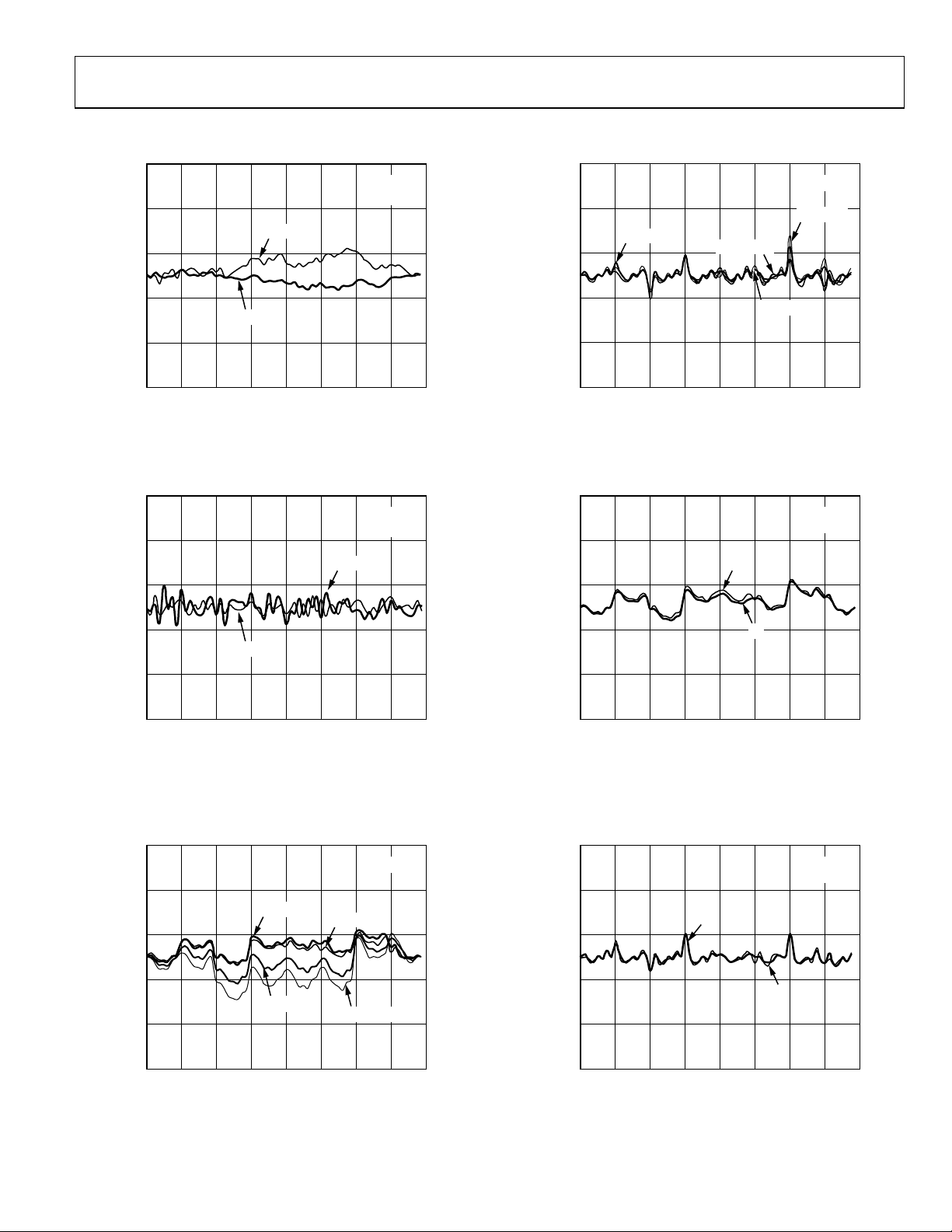
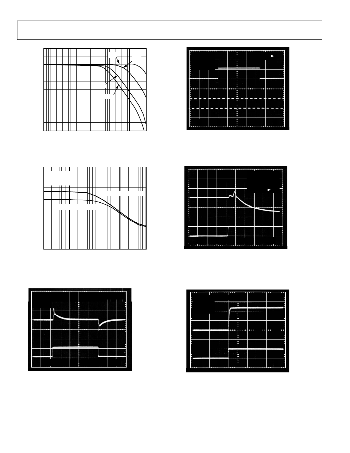
TYPICAL PERFORMANCE CHARACTERISTICS
0.5
0.3
0.1
VDD = 3V
RAB = 10kΩ
= 25°C
T
A
0.10
0.06
0.02
RAB = 10kΩ
TA = –40°C
TA = +85°C
TA = +125°C
–0.1
V
= 5V
RHEOSTAT MODE INL (LSB)
–0.3
–0.5
0648
Figure 3. R
0.25
0.15
0.05
–0.05
RHEOSTAT MODE DNL (LSB)
–0.15
–0.25
064
8
DD
16 24 32 40 48 56
CODE (Decimal)
vs. Code vs. Supply Voltages
INL
RAB = 10kΩ
= 25°C
T
A
VDD = 5V
V
= 3V
DD
16 24 32 40 48 56
CODE (Decimal)
03224-003
03224-004
–0.02
–0.06
POTENTIOMETER MODE DNL (LSB)
–0.10
0.10
0.06
0.02
–0.02
–0.06
POTENTIOMETER MODE INL (LSB)
–0.10
0648
Figure 6. DNL vs. Code vs. Temperature
0648
T
= +25°C
A
16 24 32 40 48 56
CODE (Decimal)
RAB = 10kΩ
= 25°C
T
A
3V
5V
16 24 32 40 48 56
CODE (Decimal)
03224-006
03224-007
0.10
0.06
0.02
–0.02
–0.06
POTENTIOMETER MODE INL (LSB)
–0.10
Figure 4. R
0648
vs. Code vs. Supply Voltages
DNL
TA = +85°C
T
= +25°C
A
16 24 32 40 48 56
CODE (Decimal)
Figure 5. INL vs. Code vs. Temperature
RAB = 10kΩ
TA = +125°C
TA = –40°C
03224-005
Rev. E | Page 7 of 24
0.10
0.06
0.02
–0.02
–0.06
POTENTIOMETER MODE DNL (LSB)
–0.10
Figure 7. INL vs. Code vs. Supply Voltages
3V
0648
16 24 32 40 48 56
CODE (Decimal)
Figure 8. DNL vs. Code vs. Supply Voltages
5V
RAB = 10kΩ
= 25°C
T
A
03224-008
Page 8
AD5273
0.025
0.020
0.015
0.010
0.005
POTENTIOMETER MODE LINEARITY (LSB)
0
0
SUPPLY VOLTAGE (V)
Figure 9. INL vs. Supply Voltage
TA = 25°C
= 10kΩ
R
AB
CODE = 0x20
61234 5
03224-009
1.0
0.9
0.8
0.7
0.6
0.5
ZSE (LSB)
0.4
0.3
0.2
0.1
0
–40 100–20
RAB = 10kΩ
VDD = 3V
VDD = 5V
020406080
TEMPERATURE (°C)
Figure 12. Zero-Scale Error
03224-012
0.4
TA = 25°C
= 10kΩ
R
AB
0.3
0.2
0.1
0
RHEOSTAT MODE LINEARITY (LSB)
–0.1
06
0
–0.1
–0.2
–0.3
–0.4
–0.5
FSE (LSB)
–0.6
–0.7
–0.8
–0.9
–1.0
–40 100–20
1234 5
SUPPLY VOLTAGE (V)
Figure 10. R
VDD = 3V
vs. Supply Voltage
INL
020406080
TEMPERATURE (°C)
CODE = 0x20
03224-010
RAB = 10kΩ
VDD = 5V
03224-011
Figure 11. Full-Scale Error
0.16
VDD = 5.5V
= 10kΩ
R
AB
0.14
0.12
0.10
0.08
SUPPLY CURRENT (µA)
0.06
0.04
–55 115–35 –15
Figure 13. Supply Current vs. Temperature
10
1
0.1
0.01
SUPPLY CURRENT (mA)
0.001
0.0001
061
Figure 14. Supply Current vs. Digital Input Voltage
5 25456585105
TEMPERATURE (°C)
TA = 25°C
R
= 10kΩ
AB
VDD = 5V
VDD = 2.7V
2345
INPUT LOGIC VOLTAGE (V)
ALL DIGITAL
PINS TIED
TOGETHER
03224-013
03224-014
Rev. E | Page 8 of 24
Page 9

AD5273
500
400
C)
°
300
1kΩ
200
100
0
–100
RHEOSTAT MODE TEMPCO (ppm/
–200
–300
100kΩ
0648
10kΩ
50kΩ
16 24 32 40 48 56
CODE (Decimal)
Figure 15. Rheostat Mode Tempco (∆R
WB/RWB
VDD = 5.5V
T
= 25°C
A
)/∆T vs. Code
03224-015
0
–6
–12
–18
–24
–30
MAGNITUDE (dB)
–36
–42
–48
–54
100 1M
Figure 18. Gain vs. Frequency vs. Code, R
0x3F
0x20
0x10
0x08
0x04
0x02
0x01
0x00
1k 10k 100k
FREQUENCY (Hz)
= 10 kΩ
AB
03224-018
40
)/∆T vs. Code
W/VW
= 1 kΩ
AB
VDD = 5.5V
03224-016
03224-017
30
C)
°
20
10
0
–10
–20
RHEOSTAT MODE TEMPCO (ppm/
–30
–40
064
16 24 32 40 48 56
8
1kΩ
10kΩ
50kΩ
100kΩ
CODE (Decimal)
Figure 16. Potentiometer Mode Tempco (∆V
0
–6
–12
–18
–24
–30
MAGNITUDE (dB)
0x02 0x01 0x00
–36
–42
–48
–54
100 10M
0x3F
0x20
0x10
0x08
0x04
1k 10k 100k 1M
FREQUENCY (Hz)
Figure 17. Gain vs. Frequency vs. Code, R
0
–6
–12
–18
–24
–30
MAGNITUDE (dB)
–36
–42
–48
–54
100 1M
Figure 19. Gain vs. Frequency vs. Code, R
0
–6
–12
–18
–24
–30
MAGNITUDE (dB)
–36
–42
–48
–54
100 1M
Figure 20. Gain vs. Frequency vs. Code, R
0x3F
0x20
0x10
0x08
0x04
0x02
0x01
0x00
1k 10k 100k
FREQUENCY (Hz)
= 50 kΩ
AB
0x3F
0x20
0x10
0x08
0x04
0x02
0x01
0x00
1k 10k 100k
FREQUENCY (Hz)
= 100 kΩ
AB
03224-019
03224-020
Rev. E | Page 9 of 24
Page 10
AD5273
V
12
6
0
–6
–12
–18
–24
MAGNITUDE (dB)
–30
–36
–42
–48
–80
–60
TA = 25°C
CODE = 0x20
= 2.5V, VB = V
V
A
1kΩ
50kΩ
100kΩ
1k 10k 100k 1M
FREQUENCY (Hz)
Figure 21. −3 dB Bandwidth
VDD = 5V DC ±1.0V p-p AC
10kΩ
VDD = 5.5V
V
= 5.5V
A
VB = GND
f
= 400kHz
CLK
5V 5V 5µs
03224-021
10M100
DATA 0x00 0x3F
VW = 5V/DIV
SCL = 5V/DI
03224-024
Figure 24. Large Settling Time
VDD = 5.5V
V
= 5.5V
A
V
= GND
B
f
= 100kHz
CLK
DATA 0x20 0x1F
–40
–20
POWER SUPPLY REJECTION RATIO (dB)
0
100 1M1k
VDD = 5.5V
V
= 5.5V
A
= GND
V
B
10mV
VDD = 3V DC ±0.6V p-p AC
10k 100k
FREQUENCY (Hz)
Figure 22. PSRR v s. Frequency
5V
Figure 23. Digital Feedthrough
f
CLK
= 100kHz
500ns
03224-022
= 10mV/DIV
V
W
SCL = 5V/DIV
03224-023
V
= 50mV/DIV
W
5V50mV 200ns
SCL = 5V/DIV
03224-025
Figure 25. Midscale Glitch Energy
OTP PROGRAMMED AT MS
V
= 5.5V
DD
V
= 5.5V
A
= 10kV
R
AB
= 1V/DIV
V
W
w
VDD = 5V/DIV
5V1V
5µs
03224-026
Figure 26. Power-Up Settling Time After Fuses Blown
Rev. E | Page 10 of 24
Page 11

AD5273
SDA
10
(mA)
1.0
WB_MAX
0.1
THEORETICAL I
RAB = 1k
Ω
RAB = 10k
RAB = 50k
RAB = 100k
VA = VB = OPEN
T
= 25°C
A
Ω
Ω
Ω
0.01
068
16 24 32 40 48 56
CODE (Decimal)
Figure 27. I
SCL
vs. Code
WB_MAX
t
2
t
3
t
8
t
1
PS P
03224-027
4
t
8
t
9
t
9
t
4
t
5
t
6
t
7
Figure 28. Interface Timing Diagram
t
10
03224-028
Rev. E | Page 11 of 24
Page 12

AD5273
THEORY OF OPERATION
The AD5273 is a one-time-programmable (OTP), set-andforget, 6-bit digital potentiometer. The AD5273 allows
unlimited 6-bit adjustments prior to the OTP. OTP technology
is a proven cost-effective alternative over EEMEM in one-time
memory programming applications. The AD5273 employs fuse
link technology to achieve the memory retention of the resistance
setting function. It comprises six data fuses, which control the
address decoder for programming the RDAC, one user mode
test fuse for checking setup error, and one programming lock
fuse for disabling any further programming once the data fuses
are programmed correctly.
ONE-TIME PROGRAMMING
Prior to OTP activation, the AD5273 presets to midscale during
power-on. After the wiper is set to the desired position, the
resistance can be permanently set by programming the T bit
and the one-time V
properly (see Table 4). The fuse link technology of the AD5273
to high and by coding the part
DD_OTP
requires a V
between 5.25 V and 5.5 V to blow the fuses to
DD_OTP
achieve a given nonvolatile setting. During operation, however,
can be 2.7 V to 5.5 V. Therefore, a system supply that is
V
DD
lower than 5.25 V requires an external supply for OTP. The user
is allowed only one attempt to blow the fuses. If the user fails to
blow the fuses on the first attempt, the fuse structure might
change such that they can never be blown, regardless of the
energy applied during subsequent events. For details, see the
Power Supply Considerations section.
The device control circuit has two validation bits, E1 and E0,
that can be read back in the read mode for checking the programming status, as shown in Table 5. Users should always read
back the validation bits to ensure that the fuses are properly
blown. After the fuses have been blown, all fuse latches are
enabled upon subsequent power-on; therefore, the output
corresponds to the stored setting. Figure 29 shows a detailed
functional block diagram.
SCL
SDA
2
C INTERFACE
I
COMPARATOR
ONE-TIME
PROGRAM/TEST
CONTROL BLOCK
Figure 29. Detailed Functional Block Diagram
DAC
REG.
FUSES
EN
MUX
FUSE
REG.
DECODER
A
W
B
03224-031
Table 4. SDA Write Mode Bit Format
S010110AD00ATXXXXXXXAXXD5D4D3D2D1D0AP
SLAVE ADDRESS BYTE INSTRUCTION BYTE DATA BYTE
Table 5. SDA Read Mode Bit Format
S 0 1 0 1 1 0 AD0 1 A E1 E0 D5 D4 D3 D2 D1 D0 A P
SLAVE ADDRESS BYTE DATA BYTE
03224-030
SDA Bit Definitions and Descriptions
S = start condition.
P = stop condition.
A = acknowledge.
X = don’t care.
T = OTP programming bit. Logic 1 programs wiper position
permanently.
D5, D4, D3, D2, D1, D0 = data bits.
E1, E0 = OTP validation bits.
0, 0 = ready to program.
0, 1 = test fuse not blown successfully. (For factory setup
checking purpose only. Users should not see these
combinations.)
1, 0 = fatal error. Do not retry. Discard the unit.
1, 1 = programmed successfully. No further adjustments
possible.
2
AD0 = I
C device address bit. Allows maximum of two
AD5273s to be addressed.
03224-029
Rev. E | Page 12 of 24
Page 13
AD5273
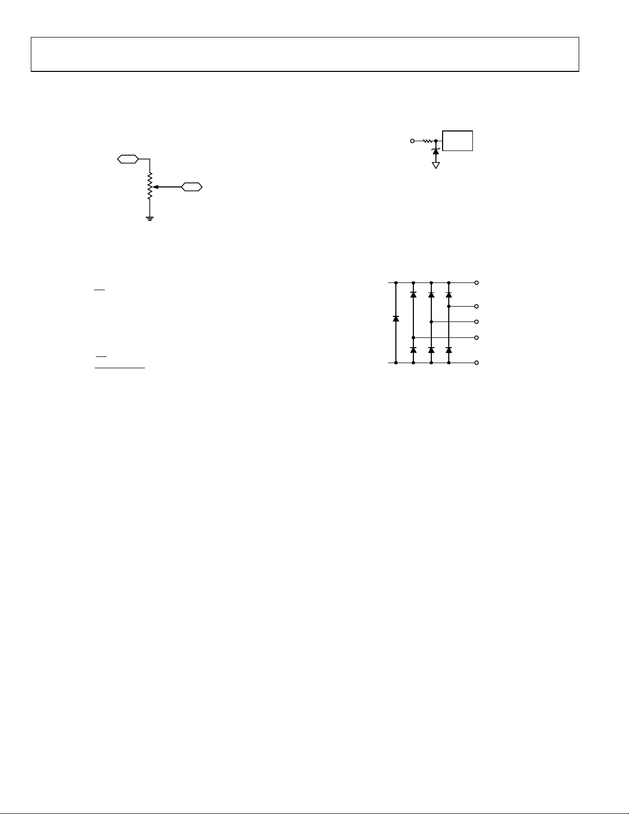
−
VARIABLE RESISTANCE AND VOLTAGE FOR RHEOSTAT MODE
If only the W-to-B or W-to-A terminals are used as variable
resistors, the unused A or B terminal can be opened or shorted
with W. This operation is called rheostat mode (see Figure 30).
Since a finite wiper resistance of 60 Ω is present in the zeroscale condition, care should be taken to limit the current flow
between W and B in this state to a maximum pulse current of
20 mA. Otherwise, degradation or possible destruction of the
internal switch contact can occur.
A
B
Figure 30. Rheostat Mode Configuration
A
W
B
A
W
W
B
03224-032
The nominal resistance, RAB, of the RDAC has 64 contact points
accessed by the wiper terminal, plus the B terminal contact if
R
is considered. The 6-bit data in the RDAC latch is decoded
WB
to select one of the 64 settings. Assuming that a 10 kΩ part is
used, the wiper’s first connection starts at Terminal B for Data
Register 0x00. This connection yields a minimum of 60 Ω
resistance between Terminals W and B because of the 60 Ω
wiper contact resistance. The second connection is the first tap
point, which corresponds to 219 Ω (R
= 1 × RAB/63 + RW) for
W
Data Register 0x01, and so on. Each LSB data value increase
moves the wiper up the resistor ladder until the last tap point is
reached at 10060 Ω (63 × R
/63 + RW). Figure 31 shows a
AB
simplified diagram of the equivalent RDAC circuit. The general
equation determining R
D
()
DR +×=
WB
63
is
WB
RR
(1)
W
AB
Similar to the mechanical potentiometer, the resistance of the
RDAC between the Wiper W and Terminal A also produces a
complementary resistance, R
. When these terminals are used,
WA
Terminal B can be opened or shorted to W. Setting the resistance
value for R
starts at a maximum value of resistance and
WA
decreases as the data loaded in the latch increases in value. The
general equation for this operation is
63
()
DR +×
Table 7. R
WA
D (Dec) R
D
=
63
RR
(2)
W
ABWA
vs. Codes: RAB =10 kΩ, Terminal B Opened
(Ω) Output State
WA
63 60 Full scale
32 4980 Midscale
1 9901 1 LSB
0 10060 Zero scale
The typical distribution of the resistance tolerance from device
to device is process-lot dependent, and it is possible to have
±30% tolerance.
A
where:
D is the decimal equivalent of the 6-bit binary code.
R
is the end-to-end resistance.
AB
R
is the wiper resistance contributed by the on resistance of
W
the internal switch.
Table 6. R
D (Dec) R
vs. Codes: RAB = 10 kΩ; Terminal A Opened
WB
(Ω) Output State
WB
63 10060 Full scale (RAB + RW)
32 5139 Midscale
1 219 1 LSB
0 60 Zero scale (wiper contact resistance)
D5
D4
D3
D2
D1
D0
RDAC
LATCH
AND
DECODER
Figure 31. AD5273 Equivalent RDAC Circuit
R
S
R
S
W
R
S
B
03224-033
Rev. E | Page 13 of 24
Page 14
AD5273
Ω
VARIABLE RESISTANCE AND VOLTAGE FOR POTENTIOMETER MODE
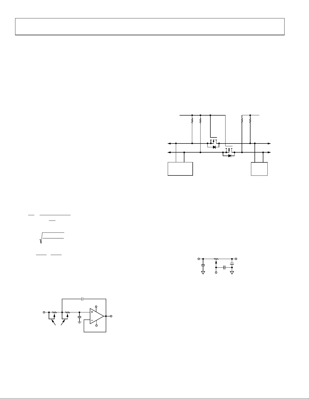
If all three terminals are used, the operation is called the
potentiometer mode. The most common configuration is
the voltage divider operation (see Figure 32).
V
I
A
W
V
O
B
03224-034
Figure 32. Potentiometer Mode Configuration
Ignoring the effect of the wiper resistance, the transfer function
is simply
D
= (3)
()
DV
W
A more accurate calculation, which includes the wiper
resistance effect, yields
()
DV
W
Unlike rheostat mode where the absolute tolerance is high,
potentiometer mode yields an almost ratiometric function of
D/63 with a relatively small error contributed by the R
Therefore the tolerance effect is almost cancelled. Although the
step resistor, R
ent temperature coefficients, the ratiometric adjustment also
reduces the overall temperature coefficient effect to 5 ppm/°C,
except at low value codes where R
Potentiometer mode includes op amp feedback resistor
networks and other voltage scaling applications. Terminals A,
W, and B can in fact be input or output terminals, provided that
|V
|, |VWA|, and |VWB| do not exceed VDD to GND.
AB
V
A
63
D
= (4)
, and CMOS switch resistor, RW, have very differ-
S
RR
+
W
AB
AB
V
A
RR
263+
W
terms.
W
dominates.
W
ESD PROTECTION
Digital inputs SDA and SCL are protected with a series input
resistor and parallel Zener ESD structures (see Figure 33).
340
LOGIC
03224-035
Figure 33. ESD Protection of Digital Pins
TERMINAL VOLTAGE OPERATING RANGE
There are also ESD protection diodes between VDD and the
RDAC terminals. The V
of AD5273 therefore defines their
DD
voltage boundary conditions (see Figure 34). Supply signals
present on Terminals A, B, and W that exceed V
are clamped
DD
by the internal forward-biased diodes.
V
DD
A
W
B
GND
03224-036
Figure 34. Maximum Terminal Voltages Set by V
DD
POWER-UP/POWER-DOWN SEQUENCES
Because of the ESD protection diodes, it is important to power
V
first before applying any voltages to Terminals A, B, and W.
DD
Otherwise, the diode is forward-biased such that VDD is powered
unintentionally and can affect the rest of the user’s circuits. The
ideal power-up sequence is in the following order: GND, V
digital inputs, and VA/VB/VW. The order of powering VA, VB, VW,
and digital inputs is not important as long as they are powered
after V
. Similarly, VDD should be powered down last.
DD
DD
,
Rev. E | Page 14 of 24
Page 15

AD5273
POWER SUPPLY CONSIDERATIONS
To minimize the package pin count, both OTP and normal
operating voltage supplies are applied to the same V
of the AD5273. The AD5273 employs fuse link technology that
requires 5.25 V to 5.5 V for blowing the internal fuses to achieve
a given setting, but normal V
can be in the range of 2.7 V to
DD
5.5 V after completing the fuse programming process. As a
result, dual voltage supplies and isolation are needed if the system
V
is lower than the required V
DD
. For successful OTP, the
DD_OTP
fuse programming supply (either an on-board regulator or
rack-mount power supply) must be rated at 5.25 V to 5.5 V and
provide a 100 mA current for 400 ms. Once fuse programming
is completed, the V
supply must be removed to allow
DD_OTP
normal operation of 2.7 V to 5.5 V; then the device reduces the
current consumption to the µA range. Figure 35 shows the
simplest implementation using a jumper. This approach saves
one voltage supply, but draws additional current and requires
manual configuration.
CONNECT J1
HERE FOR OTP
5.5V
50kΩ
250kΩ
J1
R1
R2
C1
10µF
CONNECT J1
HERE AFTER OTP
C2
1nF
V
DD
AD5273
Figure 35. Power Supply Requirement
An alternate approach for 3.5 V to 5.25 V systems is to add a
signal diode between the system supply and the OTP supply
for isolation, as shown in Figure 36.
APPLIES FOR OTP ONLY
5.5V
3.5V TO 5.25V
D1
C1
10µF
Figure 36. 5.5 V OTP Supply Isolated from the
3.5 V to 5.25 V Normal Operating Supply
C2
1nF
V
DD
AD5273
terminal
DD
03224-037
03224-038
When operating systems at 2.7 V, use of the bidirectional low
threshold P-Ch MOSFETs is recommended for the supply’s
isolation. As shown in Figure 37, this assumes that the 2.7 V
system voltage is applied first and that the P1 and P2 gates are
pulled to ground, thus turning on P1 first and then P2. As a
result, V
setting is found, the factory tester applies the V
of the AD5273 approaches 2.7 V. When the AD5273
DD
to both
DD_OTP
the VDD and the MOSFETs’ gates, thus turning off P1 and P2.
The OTP command should be executed at this time to program
the AD5273 while the 2.7 V source is protected. Once the fuse
programming is completed, the tester withdraws the V
DD_OTP
and the AD5273’s setting is fixed permanently.
APPLIES FOR OTP ONLY
5.5V
R1
10kΩ
2.7V
P2
P1
P1 = P2 = FDV302P, NDS0610
C1
10µF
C2
1nF
V
DD
AD5273
03224-039
Figure 37. 5.5 V OTP Supply Isolated From the
2.7 V Normal Operating Supply
AD5273 achieves the OTP function through blowing internal
fuses. Users should always apply the 5.25 V to 5.5 V OTP
voltage requirement at the first fuse programming attempt.
Failure to comply with this requirement can lead to a change in
fuse structures, rendering programming inoperable.
Care should be taken when SCL and SDA are driven from a low
voltage logic controller. Users must ensure that the logic high
level is between 0.7 V × V
and VDD. Refer to the Level Shift
DD
for Different Voltages section.
Poor PCB layout introduces parasitics that can affect fuse
programming. Therefore, it is recommended to add a 10 µF
tantalum capacitor in parallel with a 1 nF ceramic capacitor as
close as possible to the V
pin. The type and value chosen for
DD
both capacitors are important. This combination of capacitor
values provides a fast response and larger supply current
handling with minimum supply drop during transients. As a
result, these capacitors increase the OTP programming success
by not inhibiting the proper energy needed to blow the internal
fuses. Additionally, C1 minimizes transient disturbance and low
frequency ripple, while C2 reduces high frequency noise during
normal operation.
Rev. E | Page 15 of 24
Page 16

AD5273
CONTROLLING THE AD5273
To control the AD5273, users can program the device with
either computer software or with external I2C controllers.
SOFTWARE PROGRAMMING
Because of the OTP feature, users can program the AD5273 in
the factory before shipping it to end users. Therefore, ADI
offers device programming software that can be implemented in
the factory on computers running Windows NT, Windows 2000,
and Windows XP platforms. The software, which can be
downloaded from the AD5273 product folder at
http://www.analog.com, is an executable file that does not
require any programming languages or user programming
skills. Figure 38 shows the software interface.
Figure 38. Software Interface
Write
The AD5273 starts at midscale after power-up prior to any OTP
programming. To increment or decrement the resistance, move
the scrollbar on the left. Once the desired setting is found, click
Program Permanent to lock the setting permanently. To write
any specific values, use the bit pattern control in the upper
section and click
shown in Table 4. Once the desired setting is found, set the T bit
to 1 and click
Read
To read the validation bits and data from the device, click Read.
The user can also set the bit pattern in the upper section and
click
Run. The format of reading data from the device is shown
in Table 5.
Run. The format of writing data to the device is
Run to program the setting permanently.
To control the device in both read and write operations, the
2
program generates the I
C digital signals through the parallel
port LPT1 Pins 2, 3, 15, and 25 for SDA_write, SCL, SDA_read,
and DGND, respectively (see Figure 39).
To apply the device programming software in the factory, lay
out the AD5273 SCL and SDA pads on the PCB such that the
programming signals can be communicated to and from the
parallel port (see Figure 39). Figure 40 shows a recommended
AD5273 PCB layout into which pogo pins can be inserted for
factory programming. To prevent damaging the PC parallel
port, 100 Ω resistors should also be put in series to the SCL and
SDA pins. Pull-up resistors on SCL and SDA are also required.
13
25
12
24
11
23
10
22
9
21
8
20
7
19
6
18
5
17
03224-040
4
16
3
15
2
14
1
Figure 39. Parallel Port Connection. Pin 2 = SDA_Write, Pin 3 = SCL,
Pin 15 = SDA_Read, and Pin 25 = DGND
W
V
DD
DGND
SCL
Figure 40. Recommended AD5273 PCB Layout
R3
100Ω
V
DD
R4
10kΩR510kΩ
SCL
READ
R2
100Ω
R1
WRITE
100Ω
A
B
AD0
SDA
SDA
03224-042
03224-041
Rev. E | Page 16 of 24
Page 17

AD5273
S
Y
S
Y
S
Y
I2C CONTROLLER PROGRAMMING
Write Bit Patterns
80 8
X
X
ACK. BY
AD5273
XX
ACK. BY
AD5273
FRAME 2
RDAC REGISTER
X
8
08
X
D4 D3 D2 D1
XD5
FRAME 1
DATA BYTE
X D5D4D3D2D1
FRAME 1
DATA BYTE
D0
NO ACK. BY
AD5273
STOP BY
MASTER
D0
ACK. BY
AD5273
D0
ACK. BY
AD5273
03224-059
STOP BY
MASTER
STOP BY
MASTER
03224-043
03224-044
the read operation. The instruction byte in the write mode
follows the slave address byte. The MSB of the instruction
byte labeled T is the OTP bit. After acknowledging the
instruction byte, the last byte in the write mode is the data
byte. Data is transmitted over the serial bus in sequences of
nine clock pulses (eight data bits followed by an acknowledge bit). The transitions on the SDA line must occur during
the low period of SCL and remain stable during the high
period of SCL, as shown in Figure 41.
acknowledgment of the slave address byte. Data is transmitted over the serial bus in sequences of nine clock pulses
(slight difference from write mode, there are eight data bits
followed by a no acknowledge bit). Similarly, the transitions
on the SDA line must occur during the low period of SCL
and remain stable during the high period of SCL, as shown
in Figure 43.
condition is established by the master. A stop condition is
defined as a low-to-high transition on the SDA line while
SCL is high. In the write mode, the master pulls the SDA
R/W
ACK. BY
AD5273
80
0
X
X
INSTRUCTION BYTE
TART B
MASTER
SCL
SDA
0
001
FRAME 1
SLAVE ADDRESS BYTE
11
0
AD0
Figure 41. Writing to the RDAC Register
R/W
ACK. BY
AD5273
8
0
1
X
X
INSTRUCTION BYTE
SCL
SDA
TART B
MASTER
0
0
1
0
FRAME 1
SLAVE ADDRESS BYTE
110AD0
Figure 42. Activating One-Time Programming
Read Bit Pattern
SCL
SDA
TART B
MASTER
0
0
1
0
FRAME 1
SLAVE ADDRESS BYTE
110AD0
R/W
Figure 43. Reading Data from the RDAC Register
For users who do not use the software solution, the AD5273 can
be controlled via an I
2
C-compatible serial bus and is connected
to this bus as a slave device. Referring to Figure 41, Figure 42,
2
and Figure 43, the 2-wire I
C serial bus protocol operates as
follows:
1.
The master initiates data transfer by establishing a start
condition. A start condition is defined as a high to low
transition on the SDA line while SCL is high, as shown in
Figure 41. The byte following the start condition is the
slave address byte, which consists of six MSBs defined as
010110. The next bit is AD0; it is an I
2
C device address bit.
Depending on the states of the AD0 bits, two AD5273s can
be addressed on the same bus, as shown in Figure 44. The
W
last LSB is the R/
bit, which determines whether data is
read from or written to the slave device.
The slave address corresponding to the transmitted address
responds by pulling the SDA line low during the ninth
clock pulse (this is termed the acknowledge bit). At this
stage, all other devices on the bus remain idle while the
selected device waits for data to be written to or read from
its serial register.
X
X
X
FRAME 2
X
X
X
FRAME 2
8
08
E0 D5 D4 D3 D2 D1
E1
ACK. BY
AD5273
DATA BYTE FROM SELECTED
A write operation contains one more instruction byte than
2.
3.
In read mode, the data byte follows immediately after the
4.
When all data bits have been read or written, a stop
Rev. E | Page 17 of 24
Page 18

AD5273
line high during the 10th clock pulse to establish a stop
condition, as shown in Figure 41 and Figure 42. In the read
mode, the master issues a no acknowledge for the ninth
clock pulse, that is, the SDA line remains high. The master
then brings the SDA line low before the 10th clock pulse,
which goes high to establish a stop condition, as shown in
Figure 43.
A repeated write function gives the user flexibility to
update the RDAC output continuously, except after
permanent programming, when the part is addressed and
receives instructions only once. During the write cycle,
each data byte updates the RDAC output. For example,
after the RDAC has acknowledged its slave address and
instruction bytes, the RDAC output updates after these two
bytes. If another byte is written to the RDAC while it is still
addressed to a specific slave device with the same instruction, this byte updates the output of the selected slave device.
If different instructions are needed, the write mode must
be started again with a new slave address, instruction, and
data bytes. Similarly, a repeated read function of the RDAC
is also allowed.
CONTROLLING TWO DEVICES ON ONE BUS
Figure 44 shows two AD5273 devices on the same serial bus.
Each has a different slave address since the state of each AD0
pin is different. This allows each device to operate independently.
The master device output bus line drivers are open-drain pulldown in a fully I
2
C-compatible interface.
5V
5V
R
P
SDA
AD0
AD5273
R
P
MASTER
SCL
SDA
AD0
AD5273
Figure 44. Two AD5273 Devices on One Bus
SCL
SDA
SCL
03224-045
Rev. E | Page 18 of 24
Page 19

AD5273
A
(
)
×
APPLICATIONS
DAC
It is common to buffer the output of the digital potentiometer
as a DAC. The buffer minimizes the load dependence and
delivers higher current to the load, if needed.
5V
1U1
V
IN
V
OUT
GND
2
ADR03
Figure 45. Programmable Voltage Reference (DAC)
AD5273
3
U3
5V
A
W
AD8601
U2
V
O
03224-046
B
PROGRAMMABLE VOLTAGE SOURCE WITH BOOSTED OUTPUT
For applications that require high current adjustment, such as a
laser diode driver or tunable laser, consider a booster voltage
source, as shown in Figure 46.
AD8601
+V
U2
–V
U3 2N7002
SIGNAL
V
U1
D5273
IN
A
W
B
Figure 46. Programmable Booster Voltage Source
In this circuit, the inverting input of the op amp forces the V
V
OUT
R
BIAS
C
C
I
L
LD
03224-047
OUT
to be equal to the wiper voltage set by the digital potentiometer.
The load current is then delivered by the supply via the
N-Ch FET, N
– V
(V
IN
. N1 power handling must be adequate to dissipate
1
) × IL power. This circuit can source a maximum of
OUT
100 mA with a 5 V supply. For precision applications, a voltage
reference, such as the ADR421, ADR03, or ADR370, can be
applied at Terminal A of the digital potentiometer.
PROGRAMMABLE CURRENT SOURCE
A programmable current source can be implemented with the
circuit shown in Figure 47. The load current is the voltage
across Terminals B-to-W of the AD5273 divided by R
scale, Terminal A of the AD5273 is −2.048 V, which makes the
wiper voltage clamped at ground potential. Depending on the
load, Equation 5 is therefore valid only at certain codes. For
example, when the compliance voltage, V
, equals half of V
L
the current can be programmed from midscale to full scale of
the AD5273.
. At zero
S
REF
,
GAIN CONTROL COMPENSATION
As shown in Figure 48, the digital potentiometers are
commonly used in gain controls or sensor transimpedance
amplifier signal conditioning applications.
In both applications, one of the digital potentiometer terminals
is connected to the op amp inverting node with finite terminal
capacitance, C1. It introduces a zero for the 1 β
20 dB/dec, whereas a typical op amp GBP has −20 dB/dec
characteristics. A large R2 and finite C1 can cause this zero’s
frequency to fall well below the crossover frequency. Therefore,
the rate of closure becomes 40 dB/dec and the system has a 0°
phase margin at the crossover frequency. The output may ring,
or in the worst case, oscillate when the input is a step function.
Similarly, it is also likely to ring when switching between two
gain values because this is equivalent to a step change at the
input. To reduce the effect of C1, users should also configure
Terminal B or Terminal A rather than Terminal W at the
inverting node.
5V
3
2U1
V
S
OUPUT
SLEEP
REF191
GND
4
–2.048 + V
0 TO (2.048 + VL)
6
C1 1µF
L
U3
AD5273
+5V
U2
V+
OP1177
V–
–5V
Figure 47. Programmable Current Source
REF
= D
I
L
R
S
R1
47kΩ
C1
≤≤
4.7pF
100kΩ
B
U1
V
I
64/
DV
Figure 48. Typical Noninverting Gain Amplifier
B
W
A
R
S
102Ω
I
L
V
L
R
100Ω
L
6332|
(5)
C2
R2
A
W
V
O
03224-049
term with
o
03224-048
Rev. E | Page 19 of 24
Page 20
AD5273
S
S
2
Depending on the op amp GBP, reducing the feedback resistor
may extend the zero’s frequency far enough to overcome the
problem. A better approach is to include a compensation
capacitor, C2, to cancel the effect caused by C1. Optimum
compensation occurs when R1 × C1 = R2 × C2, but this is not
an option because of the variation of R2. As a result, users can
use the relationship described and scale C2 as if R2 were at its
maximum value. However, doing so may overcompensate by
slowing down the settling time when R2 is set to low values. To
avoid this problem, C2 should be found empirically for a given
application. In general, setting C2 in the range of a few picofarads
to no more than a few tenths of a picofarad is usually adequate
for compensation.
There is also a Terminal W capacitance connected to the output
(not shown); its effect on stability is less significant; therefore.
compensation is not necessary unless the op amp is driving a
large capacitive load.
PROGRAMMABLE LOW-PASS FILTER
In ADC applications, it is common to include an antialiasing
filter to band-limit the sampling signal. To minimize various
system redesigns, users can use two 1 kΩ AD5273s to construct
a generic second-order Sallen key low-pass filter. Since the
AD5273 is a single-supply device, the input must be dc offset
when an ac signal is applied to avoid clipping at ground. This is
illustrated in Figure 49. The design equations are
2
V
O
=
V
I
=ω
O
Q
Users can first select some convenient values for the capacitors.
To achieve maximally flat bandwidth where Q = 0.707, let C1 be
twice the size of C2 and let R1 = R2. As a result, R1 and R2 can
be adjusted to the same setting to achieve the desired bandwidth.
ω
ω
2
O
S
+
Q
1
1R2C1C2R
+=
R2C2R1C1
R1
A
V
I
ADJUSTED TO
SAME SETTINGS
O
S
11
W
(6)
2
ω+
O
(7)
(8)
C1
R2
B
A
B
C2
W
Figure 49. Salle n Key Low-Pass Filter
+2.5V
C
V+
AD8601
C
V–
U1
–2.5V
V
O
03224-050
LEVEL SHIFT FOR DIFFERENT VOLTAGES OPERATION
If the SCL and SDA signals come from a low voltage logic
controller and are below the minimum V
level (0.7 V × VDD),
IH
level shift the signals for successful read/write communication
between the AD5171 and the controller. Figure 50 shows one of
the implementations. For example, when the SDA1 is 2.5 V, M1
turns off, and the SDA2 becomes 5 V. When the SDA1 is 0 V,
M1 turns on, and the SDA2 approaches to 0 V. As a result,
proper level shifting is established. M1 and M2 should be low
threshold N-Ch power MOSFETs, such as FDV301N.
V
V
DA1
CL1
DD1
= 2.5V
CONTROLLER
Rp Rp Rp Rp
G
G
D
S
D
S
M1
M2
2.5V
Figure 50. Level Shift for Different Voltages Operation
AD5273
DD2
2.7V–5.5V
= 5V
SDA2
SCL2
RDAC CIRCUIT SIMULATION MODEL
The internal parasitic capacitances and the external capacitive
loads dominate the ac characteristics of the digital potentiometers. Configured as a potentiometer divider, the −3 dB
bandwidth of the AD5273 (1 kΩ resistor) measures 6 MHz at
half scale. Figure 17 to Figure 20 provide the large signal BODE
plot characteristics of the four available resistor versions 1 kΩ,
10 kΩ, 50 kΩ, and 100 kΩ. Figure 51 shows a parasitic simulation model. The code following Figure 51 provides a macro
model net list for the 1 kΩ device.
AB
1kΩ
C
C
A
5pF
Figure 51. Circuit Simulation Model for RDAC = 1 kΩ
Macro Model Net List for RDAC
.PARAM D = 63, RDAC = 1E3
*
.SUBCKT DPOT (A,W,B)
*
CA A 0 25E-12
RWA A W {(1-D/63)*RDAC+60}
CW W 0 55E-12
RWB W B {D/63*RDAC+60}
CB B 0 25E-12
*
.ENDS DPOT
W
C
B
25pF
55pF
W
03224-055
03224-051
Rev. E | Page 20 of 24
Page 21

AD5273
A
EVALUATION BOARD
JP5
JP3
U4
1
TEMP
2
GND
0.1µF
3
V
C3
IN
ADR03
AD5171/AD5273
V
DD
C4
0.1µF
V
DD
C1
10µF
J1
8
7
6
5
4
3
2
1
R1
10kΩR210kΩ
SCL
SDA
0.1µF
C2
1
2
3
4
U1
W
V
DD
GND
SCL
AD5170
AD0
SDA
8
A
7
B
6
5
5
TRIM
4
V
OUT
1
W
2
V
DD
3
GND
4
SCL
C5
0.1µF
U2
8
A
7
B
6
AD0
5
SDA
JP1
JP2
V
REF
A
WV
B
AGND
CP3
–IN1
CP1
JP8
IN
JP7
+IN1
–IN2
+IN2
2
3
CP5
6
5
C6
0.1µF
CP4
–IN1
CP2
8
1
U3A
4
V–
JP4
C8
0.1µF
JP6
7
OUT2
U3B
Figure 52. Evaluation Board Schematic
CP6
C7
10µF
V
CC
V+
V
DD
OUT1
OUT1
CP7
C9
10µF
V
EE
03224-056
CP2
V
DD
V
REF
V
REF
B
W
V
JP1
JP7
A
O
U2
W
B
JP2
JP3
4
U3A
2
1
V+
V–
3
11
JP4
OUT1
AD822
003224-057
Figure 53. One Possible Configuration:
Programmable Voltage Reference
03224-058
Figure 54. Evaluation Board
Rev. E | Page 21 of 24
Page 22

AD5273
R
OUTLINE DIMENSIONS
2.90 BSC
2
1.95
BSC
56
0.65 BSC
2.80 BSC
1.45 MAX
SEATING
PLANE
0.22
0.08
8°
4°
0°
0.60
0.45
0.30
1.60 BSC
PIN 1
INDICATO
1.30
1.15
0.90
0.15 MAX
847
13
0.38
0.22
COMPLIANT TO JEDEC STANDARDS MO-178BA
Figure 55. 8-Lead Small Outline Transistor Package [SOT-23]
(RJ-8)
Dimensions shown in millimeters
ORDERING GUIDE
Model Resistance R
AD5273BRJ1-R2 1 RJ-8 SOT-23 250 DYA
AD5273BRJ1-REEL7 1 RJ-8 SOT-23 3,000 DYA
AD5273BRJ10-R2 10 RJ-8 SOT-23 250 DYB
AD5273BRJ10-REEL7 10 RJ-8 SOT-23 3,000 DYB
AD5273BRJ50-R2 50 RJ-8 SOT-23 250 DYC
AD5273BRJ50-REEL7 50 RJ-8 SOT-23 3,000 DYC
AD5273BRJ100-R2 100 RJ-8 SOT-23 250 DYD
AD5273BRJ100-REEL7 100 RJ-8 SOT-23 3,000 DYD
AD5273EVAL
1
Evaluation Board
1
Users should order samples because the evaluation kit comes with a socket, but does not include the parts.
(kΩ) Package Option Package Description Quantity Branding
AB
Rev. E | Page 22 of 24
Page 23

AD5273
NOTES
Rev. E | Page 23 of 24
Page 24

AD5273
NOTES
Purchase of licensed I2C components of Analog Devices or one of its sublicensed Associated Companies conveys a license for the purchaser under the Philips I2C Patent
Rights to use these components in an I
2
C system, provided that the system conforms to the I2C Standard Specification as defined by Philips.
© 2005 Analog Devices, Inc. All rights reserved. Trademarks and
registered trademarks are the property of their respective owners.
C03224–0–1/05(E)
Rev. E | Page 24 of 24
 Loading...