

Page 1
1-/2-Channel
S
S
R
WB
R
WA
CODE – Decimal
100
064128192 256
PERCENT OF NOMINAL
END-TO-END RESISTANCE – % R
AB
75
50
25
0
www.BDTIC.com/ADI
a
FEATURES
256 Positions
AD5260 – 1-Channel
AD5262 – 2-Channel (Independently Programmable)
Potentiometer Replacement
20 k⍀, 50 k⍀, 200 k⍀
Low Temperature Coefficient 35 ppm/ⴗC
4-Wire SPI-Compatible Serial Data Input
5 V to 15 V Single-Supply; ⴞ5.5 V Dual-Supply Operation
Power ON Mid-Scale Preset
APPLICATIONS
Mechanical Potentiometer Replacement
Instrumentation: Gain, Offset Adjustment
Stereo Channel Audio Level Control
Programmable Voltage to Current Conversion
Programmable Filters, Delays, Time Constants
Line Impedance Matching
Low Resolution DAC Replacement
GENERAL DESCRIPTION
The AD5260/AD5262 provide a single- or dual-channel, 256position, digitally controlled variable resistor (VR) device.* These
devices perform the same electronic adjustment function as a
potentiometer or variable resistor. Each channel of the AD5260/
AD5262 contains a fixed resistor with a wiper contact that taps the
fixed resistor value at a point determined by a digital code loaded
into the SPI-compatible serial-input register. The resistance between
the wiper and either end point of the fixed resistor varies linearly
with respect to the digital code transferred into the VR latch. The
variable resistor offers a completely programmable value of resistance,
between the A terminal and the wiper or the B terminal and the wiper.
The fixed A to B terminal resistance of 20 kW, 50 kW, or 200 kW has
a nominal temperature coefficient of 35 ppm/∞C. Unlike the majority
of the digital potentiometers in the market, these devices can operate
up to 15 V or ± 5 V provided proper supply voltages are furnished.
Each VR has its own VR latch, which holds its programmed resistance
value. These VR latches are updated from an internal serial-to-parallel
shift register, which is loaded from a standard 3-wire serial-input
digital interface. The AD5260 contains an 8-bit serial register
while the AD5262 contains a 9-bit serial register. Each bit is clocked
into the register on the positive edge of the CLK. The AD5262
address bit determines the corresponding VR latch to be loaded
with the last 8 bits of the data word during the positive edging of
CS strobe. A serial data output pin at the opposite end of the serial
register enables simple daisy chaining in multiple VR applications
without additional external decoding logic. An optional reset pin
(PR) forces the wiper to the mid-scale position by loading 80
the VR latch.
*The terms digital potentiometers, VR, and RDAC are used interchangeably.
REV. 0
Information furnished by Analog Devices is believed to be accurate and
reliable. However, no responsibility is assumed by Analog Devices for its
use, nor for any infringements of patents or other rights of third parties that
may result from its use. No license is granted by implication or otherwise
under any patent or patent rights of Analog Devices.
15 V Digital Potentiometers
AD5260/AD5262
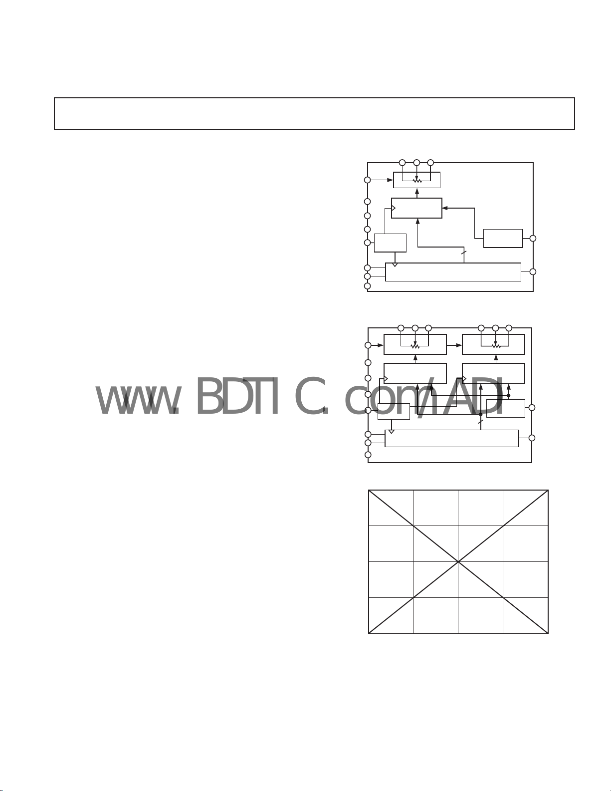
FUNCTIONAL BLOCK DIAGRAMS
AWB
HDN
V
DD
V
SS
V
L
CS
CLK
SDI
GND
HDN
V
DD
V
SS
V
L
CS
CLK
SDI
GND
into
H
RDAC
REGISTER
LOGIC
SERIAL INPUT REGISTER
A1 W1 B1
RDAC1 REGISTER
LOGIC
SERIAL INPUT REGISTER
AD5262
Figure 1. RWA and RWB vs. Code
The AD5260/AD5262 are available in thin surface-mount TSSOP-14
and TSSOP-16 packages. All parts are guaranteed to operate over
the extended industrial temperature range of –40∞C to +85∞C.
One Technology Way, P.O. Box 9106, Norwood, MA 02062-9106, U.S.A.
Tel: 781/329-4700www.analog.com
Fax: 781/326-8703 © Analog Devices, Inc., 2002
AD5260
POWER-ON
RESET
8
A2 W2 B2
RDAC2 REGISTER
POWER-ON
RESET
8
PR
SDO
PR
SDO
Page 2

(VDD = +15 V, VSS = 0 V or, VDD = +5 V, VSS = –5 V, VL = +5 V, VA = +5 V,
www.BDTIC.com/ADI
AD5260/AD5262–SPECIFICATIONS
VB = 0 V, – 40ⴗC < TA < +85ⴗC unless otherwise noted.)
ELECTRICAL CHARACTERISTICS 20 kW, 50 kW, 200 kW VERSIONS
Parameter Symbol Conditions Min Typ
DC CHARACTERISTICS RHEOSTAT MODE Specifications apply to all VRs
Resistor Differential NL
Resistor Nonlinearity
Nominal Resistor Tolerance
Resistance Temperature Coefficient R
Wiper Resistance R
Channel Resistance Matching (AD5262 only) R
Resistance Drift R
2
2
3
R-DNL RWB, VA=NC –1 ± 1/4 +1 LSB
R-INL RWB, VA=NC –1 ± 1/2 +1 LSB
R
AB
/TWiper = No Connect 35 ppm/∞C
AB
W
WB/RWB
AB
TA = 25∞C –30 30 %
IW = 1 V/R
Ch 1 and 2 R
AB
WB, DX = 80H
DC CHARACTERISTICS POTENTIOMETER DIVIDER MODE Specifications apply to all VRs
Resolution N 8 Bits
Differential Nonlinearity
Integral Nonlinearity
Voltage Divider Temperature Coefficient DV
Full-Scale Error V
Zero-Scale Error V
RESISTOR TERMINALS
Voltage Range
Capacitance
5
6
Ax, Bx C
Capacitance6 Wx C
Common-Mode Leakage Current I
Shut Down Current
4
4
7
DNL –1 ± 1/4 +1 LSB
INL –1 ± 1/2 +1 LSB
/DTCode = 80
WFSE
WZSE
V
A, B, W
A,B
W
CM
I
SHDN
W
Code = FF
Code = 00
f = 5 MHz, 25 pF
measured to GND, Code = 80
f = 1 MHz, 55 pF
measured to GND, Code = 80
VA =VB = V
H
H
H
H
/2 1 nA
DD
H
–2 –1 +0 LSB
01 2LSB
V
SS
DIGITAL INPUTS and OUTPUTS
Input Logic High V
Input Logic Low V
Input Logic High V
Input Logic Low V
Output Logic High (SDO) V
Output Logic Low (SDO) V
Input Current
Input Capacitance
8
6
IH
IL
IH
IL
OH
OL
I
IL
C
IL
VL = 3 V, VSS = 0 V 2.1 V
VL = 3 V, VSS = 0 V 0.6 V
R
IOL = 1.6 mA, V
= 2 kW to 5 V 4.9 V
PULL-UP
= 5 V 0.4 V
LOGIC
VIN = 0 V or 5 V ± 1 mA
2.4 V
POWER SUPPLIES
Logic Supply V
Power Single-Supply Range V
Power Dual-Supply Range V
Logic Supply Current I
Positive Supply Current I
Negative Supply Current I
Power Dissipation
9
L
DD RANGE
DD/SS RANGE
L
DD
SS
P
DISS
VSS = 0 V 4.5 16.5 V
VL =5 V 60 mA
VIH = 5 V or VIL = 0 V 1 mA
VSS = –5 V 1 mA
VIH = 5 V or VIL = 0 V, 0.3 mW
= +5 V, VSS = –5 V
V
DD
2.7 5.5 V
± 4.5 ± 5.5 V
Power Supply Sensitivity PSS DVDD = +5 V, ± 10% 0.003 0.01 %/%
DYNAMIC CHARACTERISTICS
6, 10
Bandwidth –3 dB BW RAB = 20 kW/50 kW/200 kW 310/130/30 kHz
Total Harmonic Distortion THD
V
Settling Time t
W
Crosstalk
11
S
C
T
W
VA = 1 V
f=1 kHz, R
VA = +5 V, VB = –5 V, 5 ms
± 1 LSB error band, R
VA = VDD, VB=0 V,
Measure V
, VB = 0 V, 0.014 %
RMS
= 20 kW
AB
= 20 kW
AB
with Adjacent
W
RDAC Making Full-Scale 1 nV–s
Code Change (AD5262 only)
Analog Crosstalk C
Resistor Noise Voltage e
TA
N_WB
VA1= VDD, VB1= 0V,
Measure V
= 5 V p-p @ f = 10 kHz, –64 dB
V
W2
R
= 20 kW/200 kW (AD5262 only)
AB
W1
with
RWB = 20 kW 13 nV/÷Hz
f = 1 kHz
1
Max Unit
60 150 W
0.1 %
0.05 %
5 ppm/∞C
V
DD
5 mA
0.8 V
5pF
V
–2–
REV. 0
Page 3

AD5260/AD5262
www.BDTIC.com/ADI
Parameter Symbol Conditions Min Typ Max Unit
INTERFACE TIMING CHARACTERISTICS apply to all parts
Clock Frequency f
Input Clock Pulsewidth t
Data Setup Time t
Data Hold Time t
CLK to SDO Propagation Delay
13
CS Setup Time t
CS High Pulsewidth t
Reset Pulsewidth t
CLK Fall to CS Rise Hold Time t
CS Rise to Clock Rise Setup t
NOTES
The AD5260/AD5262 contains 1,968 transistors. Die Size: 89 mil. × 105 mil. 9,345 sq. mil.
1
Typicals represent average readings at 25°C and VDD = +5 V, VSS = –5 V.
2
Resistor position nonlinearity error R-INL is the deviation from an ideal value measured between the maximum resistance and the minimum resistance wiper positions.
R-DNL measures the relative step change from ideal between successive tap positions. Parts are guaranteed monotonic. I
3
VAB = VDD, Wiper (VW) = No connect.
4
INL and DNL are measured at VW with the RDAC configured as a potentiometer divider similar to a voltage output D/A converter. VA = VDD and VB = 0V. DNL
specification limits of ± 1 LSB maximum are Guaranteed Monotonic operating conditions.
5
Resistor terminals A, B, W have no limitations on polarity with respect to each other.
6
Guaranteed by design and not subject to production test.
7
Measured at the Ax terminals. All Ax terminals are open-circuit in shutdown mode.
8
Worst-case supply current consumed when input all logic-input levels set at 2.4 V, standard characteristic of CMOS logic.
9
P
is calculated from (IDD ⫻ VDD). CMOS logic level inputs result in minimum power dissipation.
DISS
10
All dynamic characteristics use VDD = +5 V, VSS = –5 V, VL = +5 V.
11
Measured at a VW pin where an adjacent VW pin is making a full-scale voltage change.
12
See timing diagram for location of measured values. All input control voltages are specified with tR=tF= 2ns (10% to 90% of 3 V) and timed from a voltage level of 1.5 V.
Switching characteristics are measured using VL = 5 V.
13
Propagation delay depends on value of VDD, RL, and CL.
Specifications subject to change without notice.
CLK
CH
DS
DH
t
PD
CSS
CSW
RS
CSH
CS1
, t
CL
6, 12
25 MHz
Clock level high or low 20 ns
10 ns
10 ns
RL = 1 kΩ, CL < 20pF 1 160 ns
5ns
20 ns
50 ns
0ns
10 ns
= VDD/R for both VDD= +5 V, VSS=–5V.
W
ABSOLUTE MAXIMUM RATINGS
(TA = 25°C, unless otherwise noted.)
1
VDD to GND . . . . . . . . . . . . . . . . . . . . . . . . . . –0.3 V, +15 V
V
to GND . . . . . . . . . . . . . . . . . . . . . . . . . . . . . . . 0 V, –7 V
SS
V
to VSS . . . . . . . . . . . . . . . . . . . . . . . . . . . . . . . . . . . . 15 V
DD
V
, VB, VW to GND . . . . . . . . . . . . . . . . . . . . . . . . . . VSS, V
A
AX – BX, AX – WX, BX – W
X
DD
Intermittent2 . . . . . . . . . . . . . . . . . . . . . . . . . . . . . ± 20 mA
Continuous . . . . . . . . . . . . . . . . . . . . . . . . . . . . . . . ± 5 mA
Digital Inputs and Output Voltage to GND . . . . . . . 0 V, 7 V
Operating Temperature Range . . . . . . . . . . . . –40°C to +85°C
Maximum Junction Temperature (T
) . . . . . . . . . . . 150°C
J MAX
Storage Temperature . . . . . . . . . . . . . . . . . . –65°C to +150°C
Lead Temperature (Soldering, 10 sec) . . . . . . . . . . . . 300°C
Vapor Phase (60 sec) . . . . . . . . . . . . . . . . . . . . . . . . 215°C
Infrared (15 sec) . . . . . . . . . . . . . . . . . . . . . . . . . . . 220°C
Thermal Resistance
3
θ
JA
TSSOP-14 . . . . . . . . . . . . . . . . . . . . . . . . . . . . . . 206°C/W
TSSOP-16 . . . . . . . . . . . . . . . . . . . . . . . . . . . . . . 150°C/W
NOTES
1
Stresses above those listed under Absolute Maximum Ratings may cause permanent
damage to the device. This is a stress rating only; functional operation of the device
at these or any other conditions above those listed in the operational sections of this
specification is not implied. Exposure to absolute maximum rating conditions for
extended periods may affect device reliability.
2
Maximum terminal current is bounded by the maximum current handling of the
switches, maximum power dissipation of the package, and maximum applied
voltage across any two of the A, B, and W terminals at a given resistance setting.
3
Package Power Dissipation = (T
J MAX
– TA)/ θ
JA
REV. 0
–3–
Page 4

AD5260/AD5262
WARNING!
ESD SENSITIVE DEVICE
www.BDTIC.com/ADI
ORDERING GUIDE
Package Package No. of Parts Branding
Model R
AD5260BRU20 20 –40∞C to +85∞CTSSOP-14 RU-14 96 AD5260B20
AD5260BRU20-REEL7 20 –40∞C to +85∞CTSSOP-14 RU-14 1000 AD5260B20
AD5260BRU50 50 –40∞C to +85∞CTSSOP-14 RU-14 96 AD5260B50
AD5260BRU50-REEL7 50 –40∞C to +85∞CTSSOP-14 RU-14 1000 AD5260B50
AD5260BRU200 200 –40∞C to +85∞CTSSOP-14 RU-14 96 AD5260B200
AD5260BRU200-REEL7 200 –40∞C to +85∞CTSSOP-14 RU-14 1000 AD5260B200
AD5262BRU20 20 –40∞C to +85∞CTSSOP-16 RU-16 96 AD5262B20
AD5262BRU20-REEL7 20 –40∞C to +85∞CTSSOP-16 RU-16 1000 AD5262B20
AD5262BRU50 50 –40∞C to +85∞CTSSOP-16 RU-16 96 AD5262B50
AD5262BRU50-REEL7 50 –40∞C to +85∞CTSSOP-16 RU-16 1000 AD5262B50
AD5262BRU200 200 –40∞C to +85∞CTSSOP-16 RU-16 96 AD5262B200
AD5262BRU200-REEL7 200 –40∞C to +85∞CTSSOP-16 RU-16 1000 AD5262B200
*
Line 1 contains part number, line 2 contains differentiating detail by part type and ADI logo symbol, line 3 contains date code YWW.
CAUTION
ESD (electrostatic discharge) sensitive device. Electrostatic charges as high as 4000 V readily
accumulate on the human body and test equipment and can discharge without detection. Although
the AD5260/AD5262 features proprietary ESD protection circuitry, permanent damage may occur
on devices subjected to high-energy electrostatic discharges. Therefore, proper ESD precautions
are recommended to avoid performance degradation or loss of functionality.
(kW) Temperature Description Option per Container Information
AB
*
–4–
REV. 0
Page 5
AD5260/AD5262
www.BDTIC.com/ADI
Table I. AD5260 8-Bit Serial-Data Word Format
DATA
B7 B6 B5 B4 B3 B2 B1 B0
D7 D6 D5 D4 D3 D2 D1 D0
MSB LSB
7
2
1
CLK
V
OUT
SDI
CS
0
1
0
1
0
1
0
D7 D6 D5 D4 D3 D2 D1 D0
RDAC REGISTER LOAD
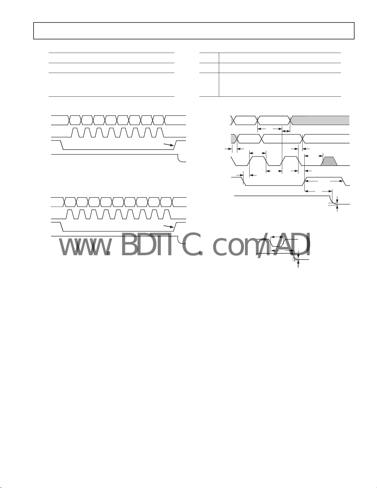
Figure 2a. AD5260 Timing Diagram
1
CLK
V
SDI
CS
OUT
0
1
0
1
0
1
0
D7 D6 D5 D4 D3 D2 D1 D0A0
RDAC REGISTER LOAD
Figure 2b. AD5262 Timing Diagram
Table II. AD5262 9-Bit Serial-Data Word Format
ADDR DATA
B8 B7 B6 B5 B4 B3 B2 B1 B0
A0 D7 D6 D5 D4 D3 D2 D1 D0
0
2
8
2
(DATA OUT)
MSB LSB
7
2
1
SDI
(DATA IN)
SDO
CLK
CS
V
OUT
Ax OR Dx Dx
0
1
ⴕ
x OR DⴕxDⴕx
A
0
1
0
1
0
V
DD
0V
t
DH
t
DS
t
CH
t
CL
t
CSS
ⴞ1 LSB ERROR BAND
t
PD_MAX
t
CS1
t
CSH
0
2
t
CSW
t
S
ⴞ1 LSB
Figure 2c. Detail Timing Diagram
PR
V
OUT
1
0
V
DD
0V
ⴞ1 LSB ERROR BAND
t
RS
t
S
ⴞ1 LSB
Figure 2d. Preset Timing Diagram
REV. 0
–5–
Page 6
AD5260/AD5262
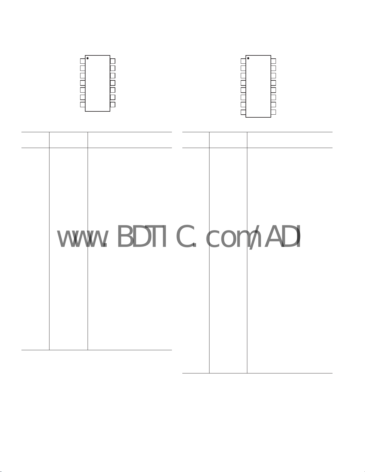
TOP VIEW
(Not to Scale)
1
2
3
4
5
6
7
8
A2
A1
W1
V
DD
SHDN
CLK
SDI
SDO
V
L
V
SS
AD5262
16
15
14
13
12
11
10
9
GND
PR
CS
B1
B2
W2
www.BDTIC.com/ADI
AD5260 PIN CONFIGURATION
SDO
14
NC
13
V
12
L
V
11
SS
10
GND
9
PR
8
CS
V
SHDN
CLK
SDI
A
W
B
DD
1
2
3
AD5260
4
TOP VIEW
5
(Not to Scale)
6
7
AD5260 PIN FUNCTION DESCRIPTIONS
Pin
Number Mnemonic Description
1A A Terminal
2W Wiper Terminal
3B B Terminal
4V
DD
Positive power supply, specified
for operation at both 5 V or 15 V.
(Sum of |V
| + |VSS| £ 15 V)
DD
5 SHDN Active low input. Terminal A
open-circuit. Shutdown controls.
Variable Resistors of RDAC.
6 CLK Serial Clock Input, positive edge
triggered.
7 SDI Serial Data Input
8 CS Chip Select Input, Active Low.
When CS returns high, data will
be loaded into the RDAC register.
9 PR Active low preset to mid-scale; sets
RDAC registers to 80
.
H
10 GND Ground
11 V
SS
Negative Power Supply, specified
for operation from 0 V to –5 V.
12 V
L
Logic Supply Voltage, needs to be
same voltage as the digital logic
controlling the AD5260.
13 NC No Connect (Users should not
connect anything other than dummy
pad on this pin)
14 SDO Serial Data Output, Open Drain
transistor requires pull-up resistor.
AD5262 PIN CONFIGURATION
AD5262 PIN FUNCTION DESCRIPTIONS
Pin
Number Mnemonic Description
1SDO Serial Data Output, Open Drain
transistor requires pull-up resistor.
2A1A Terminal RDAC #1
3W1 Wiper RDAC #1, address A0 = 0
2
4B1B Terminal RDAC #1
5V
DD
Positive power supply, specified for
operation at both 5 V or 15 V.
(Sum of |V
|+|VSS|£ 15 V)
DD
6 SHDN Active low input. Terminal A
open-circuit. Shutdown controls
Variable Resistors #1 through #2.
7 CLK Serial Clock Input, positive edge
triggered.
8 SDI Serial Data Input.
9 CS Chip Select Input, Active Low.
When CS returns high, data in
the serial input register is decoded,
based on the address Bit A0, and
loaded into the target RDAC register.
10 PR Active low preset to mid-scale sets
RDAC registers to 80
.
H
11 GND Ground
12 V
SS
Negative Power Supply, specified
for operation at both 0 V or –5 V
13 V
(Sum of |V
L
Logic Supply Voltage, needs to be
| + |VSS| <15 V).
DD
same voltage as the digital logic
controlling the AD5262.
14 B2 B Terminal RDAC #2
15 W2 Wiper RDAC #2, address A0 = 1
2
16 A2 A Terminal RDAC #2
–6–
REV. 0
Page 7

AD5260/AD5262
www.BDTIC.com/ADI
THEORY OF OPERATION
The AD5260/AD5262 provide a single- or dual-channel, 256-position
digitally controlled variable resistor (VR) device and operate up to
15 V maximum voltage. Changing the programmed VR settings
is accomplished by clocking an 8-/9-bit serial data word into the
SDI (Serial Data Input) pin. For the AD5262, the format of this
data word is one address bit. A0 represents the first bit B8, then
followed by eight data bits B7–B0 with MSB first. Tables I and II
provide the serial register data word format. See Table III for the
AD5262 address assignment to decode the location of the VR latch
receiving the serial register data in bits B7 through B0. VR outputs
can be changed one at a time in random sequence. The AD5260/
AD5262 presets to a mid-scale, simplifying fault condition recovery at power-up. Mid-scale can also be achieved at any time by
asserting the PR pin. Both parts have an internal power ON preset
that places the wiper in a mid-scale preset condition at power ON.
Operation of the power ON preset function depends only on the
state of the V
L
pin.
The AD5260/AD5262 contains a power shutdown SHDN pin,
which places the RDAC in an almost zero power consumption
state where terminals Ax are open circuited, and the wiper W is connected to B, resulting in only leakage currents being consumed in
the VR structure. In the shutdown mode, the VR latch settings are
maintained so that, returning to operational mode from power
shutdown, the VR settings return to their previous resistance values.
Table III. AD5262 Address Decode Table
A0 Latch Loaded
0 RDAC#1
1 RDAC#2
DIGITAL INTERFACING
The AD5260/AD5262 contains a 4-wire SPI-compatible
digital interface (SDI, SDO, CS, and CLK). For the AD5260,
the 8-bit serial word must be loaded with MSB first, and the
format of the word is shown in Table I. For the AD5262, the
9-bit serial word must be loaded with address bit A0 first, then
MSB of the data. The format of the word is shown in Table II.
CS
CLK
SDI
SDO
PR
GND
V
L
RDAC
LATCH
#1
PR
RDAC
LATCH
#2
PR
A0
SER
REG
D7
D6
D5
D4
D3
D2
D1
D0
POWER-
ON
PRESET
EN
ADDR
DEC
V
DD
A1
W1
B1
A2
W2
B2
SHDN
V
SS
Figure 3. AD5262 Block Diagram
The positive-edge sensitive CLK input requires clean transitions
to avoid clocking incorrect data into the serial input register.
Standard logic families work well. If mechanical switches are used
for product evaluation, they should be debounced by a flip-flop or
other suitable means. Figure 3 shows more detail of the internal
digital circuitry. When CS is low, the clock loads data into the
serial register on each positive clock edge (see Table IV).
Table IV. Truth Table
CLK CS PR SHDN Register Activity
LLHH No SR effect, enables SDO pin
≠* LH HShift one bit in from the SDI pin.
The eighth previously entered bit is
shifted out of the SDO pin.
X ≠ HH Load SR data into RDAC latch
XHHH No Operation
XXLH Sets all RDAC latches to Mid-Scale,
wiper centered, and SDO latch
cleared.
XH≠ HLatches all RDAC latches to 80
.
H
XHHL Open circuits all resistor A–terminals,
connects W to B, turns off SDO
output transistor.
*≠ = positive edge, X = don’t care, SR = shift register
The data setup and data hold times in the specification table
determine the data valid time requirements. The AD5260 uses
an 8-bit serial input data register word that is transferred to the
internal RDAC register when the CS line returns to logic high.
For the AD5262 the last 9 bits of the data word entered into the
serial register are held when CS returns high. Any extra bits are
ignored. At the same time CS goes high, it gates the address
decoder enabling AD5262 one of two positive edge-triggered
AD5262 RDAC latches (see Figure 4).
AD5260/AD5262
CLK
SDI
CS
ADDR
DECODE
SERIAL
REGISTER
RDAC 1
RDAC 2
Figure 4. Equivalent Input Control Logic
The target RDAC latch is loaded with the last 8 bits of the serial data
word completing one RDAC update. For the AD5262, two separate
9-bit data words must be clocked in to change both VR settings.
During shutdown (SHDN) the SDO output pin is forced to the
off (logic high state) to disable power dissipation in the pull-up
resistor. See Figure 5 for equivalent SDO output circuit schematic.
SHDN
CS
SDI
CLK
PR
SERIAL
REGISTER
DQ
RS
CK
SDO
Figure 5. Detail SDO Output Schematic of the AD5260
REV. 0
–7–
Page 8

AD5260/AD5262
www.BDTIC.com/ADI
All digital inputs are protected with a series input resistor and
parallel Zener ESD structure as shown in Figure 6. This applies
to digital input pins CS, SDI, SDO, PR, SHDN, and CLK.
340⍀
LOGIC
Figure 6. ESD Protection of Digital Pins
A, B, W
V
SS
Figure 7. ESD Protection of Resistor Terminals
LAYOUT AND POWER SUPPLY BYPASSING
It is a good practice to employ compact, minimum-lead length
layout design. The leads to the input should be as direct as possible
with a minimum conductor length. Ground paths should
have low resistance and low inductance.
Similarly, it is also a good practice to bypass the power supplies
with quality capacitors for optimum stability. Supply leads to the
device should be bypassed with 0.01 mF–0.1 mF disc or chip ceram-
ics
capacitors. Low-ESR 1 mF to 10 mF tantalum or electrolytic
capaci
tors should also be applied at the supplies to minimize any
transient
disturbance (see Figure 8). Notice the digital ground
should also be joined remotely to the analog ground to minimize
the ground bounce.
V
DD
V
SS
ⴙ
C1
C3
10F
0.1F
ⴙ
C2
C4
10F
0.1F
V
DD
V
GND
SS
of this data sheet. An internal level shift circuit ensures that the
common-mode voltage range of the three terminals extends
from V
SS
to V
regardless of the digital input level.
DD
POWER-UP SEQUENCE
Since there are diodes to limit the voltage compliance at terminals A, B, and W (see Figure 9), it is important to power V
DD/VSS
first before applying any voltage to terminals A, B, and W. Otherwise, the diode will be forward biased such that V
DD/VSS
will be
powered unintentionally and may affect the rest of the user’s circuit.
The ideal power-up sequence is in the following order: GND,
V
, VSS, VL, Digital Inputs, and V
DD
V
, VB, VW, and Digital Inputs is not important as long as they
A
are powered after V
DD/VSS
.
. The order of powering
A/B/W
Daisy-Chain Operation
The serial-data output (SDO) pin contains an open drain
n-channel FET. This output requires a pull-up resistor to transfer data to the next package’s SDI pin. This allows for daisy
chaining several RDACs from a single processor serial data line.
The pull-up resistor termination voltage can be larger than the V
DD
supply voltage. It is recommended to increase the Clock period
when using a pull-up resistor to the SDI pin of the following device
in series because capacitive loading at the daisy-chain node
SDO-SDI between devices may induce time delay to subsequent
devices. Users should be aware of this potential problem to achieve
data transfer successfully (see Figure 10). If two AD5260s are daisychained, this requires a total of 16 bits of data. The first 8 bits,
complying with the format shown in Table I, go to U2, and the
second 8 bits with the same format go to U1. The CS should be
kept low until all 16 bits are clocked into their respective serial
registers, and the CS is then pulled high to complete the operation.
V
DD
SCLK SS
AD5260 AD5260
U1
CLK
CS
R
P
2.2k⍀
SDOSDIMOSIC
CS
U2
SDOSDI
CLK
Figure 8. Power Supply Bypassing
TERMINAL VOLTAGE OPERATING RANGE
Figure 10. Daisy-Chain Configuration
The AD5260/AD5262 positive VDD and negative VSS power
supply defines the boundary conditions for proper 3-terminal
digital potentiometer operation. Supply signals present on terminals A, B, and W that exceed V
or VSS will be clamped by the
DD
internal forward biased diodes (see Figure 9).
V
DD
A
W
B
V
SS
Figure 9. Maximum Terminal Voltages Set by VDD and V
The ground pin of the AD5260/AD5262 device is primarily used
as a digital ground reference, which needs to be tied to the PCB’s
common ground. The digital input control signals to the AD5260/
AD5262 must be referenced to the device ground pin (GND),
RDAC STRUCTURE
The RDAC contains a string of equal resistor segments, with an
array of analog switches, that act as the wiper connection. The
number of positions is the resolution of the device. The AD5260/
AD5262 have 256 connection points allowing it to provide better
than 0.4% set-ability resolution. Figure 11 shows an equivalent
structure of the connections between the three terminals that
make up one channel of the RDAC. The SW
always be ON, while one of the switches SW(0) to SW(2
will be ON one at a time depending on the resistance position
decoded from the data bits. Since the switch is not ideal, there is
a 60 W wiper resistance, R
supply voltage and temperature. The lower the supply voltage, the
SS
higher the wiper resistance. Similarly, the higher the temperature,
. Wiper resistance is a function of
W
the higher the wiper resistance. Users should be aware of the
contribution of the wiper resistance when accurate prediction of
the output resistance is needed.
and must satisfy the logic level defined in the specification table
–8–
and SWB will
A
N
– 1)
REV. 0
Page 9

AD5260/AD5262
S
R
WB
R
WA
R
AB
= 20K⍀
D – CODE in decimal
20
064128192 256
R
WA
(D), R
WB
(D) ⴚ k⍀
16
12
8
4
0
www.BDTIC.com/ADI
Ax
HDN
RS
Note that in the zero-scale condition a finite wiper resistance of
60 W is present. Care should be taken to limit the current flow
between W and B in this state to no more than 20 mA to avoid
degradation or possible destruction of the internal switches.
R
D7
D6
D5
D4
D3
D2
D1
D0
S
Like the mechanical potentiometer the RDAC replaces, the
AD5260/AD5262 parts are totally symmetrical. The resistance
R
S
between the wiper W and terminal A also produces a digitally
controlled complementary resistance R
Wx
symmetrical programmability of the various terminal connections.
When R
is used, the B–terminal can be let floating or tied to the
WA
wiper. Setting the resistance value for R
value of resistance and decreases as the data loaded in the latch
RDAC
LATCH
AND
DECODE
DIGITAL CIRCUITRY
OMITTED FOR CLARITY
RS
= RAB/2
R
S
Bx
N
Figure 11. Simplified RDAC Architecture
PROGRAMMING THE VARIABLE RESISTOR
Rheostat Operation
The nominal resistances of the RDAC between terminals A and B
are available with values of 20 kW, 50 kW, and 200 kW. The final
three digits of the part number determine the nominal resistance
value, e.g., 20 kW = 20; 50 kW = 50; 200 kW = 200. The nominal
resistance (R
) of the VR has 256 contact points accessed by the
AB
wiper terminal, plus the B terminal contact. The 8-bit data in the
is increased in value. The general equation for this operation is:
D
-
RD
WA AB W
For example, R
256
=
()
AB
¥+
256
= 20 kW, when VA = 0 V and B–terminal is open,
the following output resistance R
RDAC latch codes. The result will be the same if terminal B is
tied to W:
DR
(DEC) (W)Output State
256 60 Full-Scale
128 10060 Mid-Scale
1 19982 1 LSB
0 20060 Zero-Scale
RDAC latch is decoded to select one of the 256 possible settings.
Assuming a 20 kW part is used, the wiper’s first connection starts
at the B terminal for data 00
. Since there is a 60 W wiper contact
H
resistance, such connection yields a minimum of 60 W resistance
between terminals W and B. The second connection is the first tap
point corresponds to 138 W (R
for data 01
. The third connection is the next tap point represent-
H
ing 216 W (78 2 60) for data 02
= RAB/256 RW = 78 W 60 W)
WB
and so on. Each LSB data
H
value increase moves the wiper up the resistor ladder until the last
tap point is reached at 19982 W [R
1 LSB RW]. The wiper
AB
does not directly connect to the B terminal. See Figure 11 for a
simplified diagram of the equivalent RDAC circuit.
The general equation determining the digitally programmed
output resistance between W and B is:
RD
WB AB W
D
256
RR
=¥+
()
where D is the decimal equivalent of the binary code which is
loaded in the 8-bit RDAC register, and R
is the nominal end-
AB
to-end resistance.
For example, R
= 20 kW, when VB = 0 V and A–terminal is
AB
open circuit, the following output resistance values R
set for the following RDAC latch codes. The result will be the
same if terminal A is tied to W:
DR
WB
(DEC) (W)Output State
256 19982 Full-Scale (R
– 1 LSB + RW)
AB
128 10060 Mid-Scale
1 138 1 LSB
060Zero-Scale (wiper contact resistance)
REV. 0
will be
WB
(1)
Figure 12. AD5260/AD5262 Equivalent RDAC Circuit
The typical distribution of the nominal resistance RAB from
channel to channel matches within ± 1%. Device-to-device matching is process lot dependent with the worst case of ± 30% variation.
On the other hand, since the resistance element is processed in
thin film technology, the change in R
low 35 ppm/∞C temperature coefficient.
–9–
RR
will be set for the following
WA
WA
AB
. Figure 12 shows the
WA
starts at a maximum
WA
(2)
with temperature has a
Page 10

AD5260/AD5262
CODE – Decimal
POTENTIOMETER MODE INL – LSB
0 256
–1.0
32 64 96 128 160 192 224
–0.8
–0.4
–0.2
0.2
0.6
1.0
–0.6
0
0.4
0.8
VDD = ⴙ5V
V
SS
= ⴚ5V
R
AB
= 20k⍀
TA = ⴙ25ⴗC
T
A
= ⴚ40ⴗC
T
A
= ⴙ125ⴗC
T
A
= ⴙ85ⴗC
www.BDTIC.com/ADI
—Typical Performance Characteristics
0.8
0.7
0.6
0.5
0.4
0.3
0.2
0.1
0
RHEOSTAT MODE INL – LSB
–0.1
–0.2
0 256
ⴞ5V
32 64 96 128 160 192 224
CODE – Decimal
ⴙ12V
TPC 1. R-INL vs. Code vs.
Supply Voltages
0.5
0.4
0.3
T
= ⴚ40ⴗC
0.2
0.1
–0.1
–0.2
–0.3
POTENTIOMETER MODE DNL – LSB
–0.4
–0.5
A
T
= ⴙ25ⴗC
T
A
0
0 256
32 64 96 128 160 192 224
CODE – Decimal
= ⴙ85ⴗC
A
TA = ⴙ125ⴗC
TPC 4. DNL vs. Code,
DD/VSS
= ±5 V
V
ⴙ5V
ⴙ15V
0.10
ⴙ12V
0.05
0
–0.05
–0.10
–0.15
RHEOSTAT MODE DNL – LSB
–0.20
–0.25
0 256
32 64 96 128 160 192 224
ⴙ5V
CODE – Decimal
TPC 2. R-DNL vs. Code vs.
Supply Voltages
0.3
0.2
0.1
0
–0.1
–0.2
–0.3
POTENTIOMETER MODE INL – LSB
–0.4
0 25632 64 96 128 160 192 224
ⴞ5V
ⴙ5V
ⴙ15V
CODE – Decimal
TPC 5. INL vs. Code vs.
Supply Voltages
ⴞ5V
ⴙ15V
TPC 3. INL vs. Code, VDD/VSS = ±5 V
0.5
0.4
0.3
0.2
ⴞ5V
0.1
0
–0.1
–0.2
–0.3
POTENTIOMETER MODE DNL – LSB
–0.4
–0.5
0 25632 64 96 128 160 192 224
ⴙ5V
CODE – Decimal
ⴙ15V
TPC 6. DNL vs. Code vs.
Supply Voltages
1.0
0.5
0
–0.5
POTENTIOMETER MODE INL – LSB
–1.0
0 20
TPC 7. INL vs. Supply Voltages
AVG +3
AVG
AVG –3
51015
VDD – VSS – V
2.0
1.5
1.0
0.5
0
–0.5
–1.0
RHEOSTAT MODE INL – LSB
–1.5
–2.0
0 20
AVG +3
AVG
AVG –3
51015
VDD – VSS – V
TPC 8. R-INL vs. Supply Voltages
–10–
124
104
84
64
44
WIPER RESISTANCE – ⍀
24
4
TPC 9. Wiper ON Resistance vs.
Bias Voltage
RON @ VDD/VSS = ⴙ5V/0V
@ VDD/VSS = ⴙ5V/ⴚ5V
R
ON
RON @ VDD/VSS = ⴙ15V/0V
ⴚ5 15
ⴚ13 11
7
V
– V
DD
REV. 0
Page 11

AD5260/AD5262
www.BDTIC.com/ADI
0
–0.5
VDD/VSS = +15V/0V
–1.0
= ⴞ5V
V
–1.5
FSE – LSB
–2.0
–2.5
–40 100
–20 20 80
060
TEMPERATURE – ⴗC
DD/VSS
VDD/VSS = +5V/0V
40
TPC 10. Full-Scale Error
28.0
27.5
27.0
26.5
– A
26.0
LOGIC
I
25.5
25.0
24.5
–40 125
TPC 13. I
VDD/VSS = +15V/0V
VDD/VSS = ⴞ5V
–7 26 92
TEMPERATURE – ⴗC
LOGIC
59
vs. Temperature
2.5
2.0
1.5
1.0
ZSE – LSB
0.5
0
–40 100
VDD/VSS = +5V/0V
= ⴞ5V
V
DD/VSS
VDD/VSS = +15V/0V
–20 20 80
TEMPERATURE – ⴗC
40060
TPC 11. Zero-Scale Error
1k
V
= 5V/0V V
DD/VSS
– A
100
LOGIC
I
VDD/VSS = 5V/0V V
10
1234
0 5
TPC 14. I
LOGIC
VIH – V
vs. Digital Input
LOGIC
= 3V
LOGIC
= 5V
Voltage
1
V
= ⴙ5V
LOGIC
V
= ⴙ5V
IH
V
= 0V
IL
0.1
0.01
SUPPLY CURRENT – A
SS
/I
DD
I
0.001
–40 125
VDD/VSS = ⴙ15V/0V
VDD/VSS = ⴞ5V
–7 26 92
TEMPERATURE – ⴗC
59
TPC 12. Supply Current vs.
Temperature
80
70
60
50
20k⍀
40
30
20
10
–10
RHEOSTAT MODE TEMPCO – ppm/ⴗC
–20
50k⍀
0
200k⍀
0 256
64 96 160 224
CODE – Decimal
19212832
TPC 15. Rheostat Mode Tempco
D
RWB/DT vs. Code
120
100
50k⍀
80
60
20k⍀
40
20
0
–20
200k⍀
–40
POTENTIOMETER MODE TEMPCO – ppm/ⴗC
–60
0 256
64 96 160 224
CODE – Decimal
19212832
TPC 16. Potentiometer Mode
D
VWB/DT vs. Code
6
TA = 25ⴗC
0
–6
–12
–18
–24
GAIN – dB
–30
–36
–42
–48
–54
1k 1M
CODE = FF
10k 100k
FREQUENCY – Hz
H
80
H
40
H
20
H
10
H
08
H
04
H
02
H
01
H
TPC 17. Gain vs. Frequency vs.
= 20 k
Code, R
AB
W
REV. 0
–11–
Page 12

AD5260/AD5262
www.BDTIC.com/ADI
6
TA = 25ⴗC
0
–6
–12
–18
–24
–30
GAIN – dB
–36
–42
–48
–54
1k 1M
CODE = FF
10k 100k
FREQUENCY – Hz
H
80
H
40
H
20
H
10
H
08
H
04
H
02
H
01
H
TPC 18. Gain vs. Frequency vs. Code
R
= 50 k
AB
NORMALIZED GAIN FLATNESS – 0.1dB/DIV
W
CODE = 80
VDD/V
T
0dB
100 100k1k 10k
= 25ⴗC
A
SS
H
= ⴞ5V
R = 200k⍀
R = 50k⍀
FREQUENCY – Hz
R = 20k⍀
6
TA = 25ⴗC
0
–6
–12
–18
–24
–30
GAIN – dB
–36
–42
–48
–54
1k 100k
CODE = FF
FREQUENCY – Hz
80
40
20
10
08
04
02
01
10k
H
H
H
H
H
H
H
H
H
TPC 19. Gain vs. Frequency vs.
Code R
600
500
400
– A
300
LOGIC
I
200
100
0
10k 10M
= 200 k
AB
VDD/VSS = +5V/0V
100k
FREQUENCY – Hz
W
V
DD/VSS
CODE FF
= ⴞ5V
CODE 55
1M
6
0
–6
–12
–18
f
–3dB
–24
–30
GAIN – dB
–36
–42
–48
–3dB
BANDWIDTHS
–54
1k 1M
f
= 310kHz, R = 20k⍀
f
–3dB
= 30kHz, R = 200k⍀
–3dB
= 131kHz, R = 50k⍀
10k 100k
FREQUENCY – Hz
VIN = 50mV rms
= ⴞ5V
V
DD/VSS
TPC 20. –3 dB Bandwidth
600
H
H
500
400
300
PSRR – dB
200
100
0
100 1M
CODE = 80
–PSRR @ VDD = ⴞ5V DC ⴞ 10% p-p AC
+PSRR @ V
1k
FREQUENCY – Hz
, VA = VDD, VB = 0V
H
= ⴞ5V DC ⴞ 10% p-p AC
DD
10k
100k
TPC 21. Normalized Gain
Flatness vs. Frequency
20mV/DIV
5V/DIV
1s/DI V
TPC 24. Mid-Scale Glitch
Energy, Code 80
to 7F
H
TPC 22. I
5V/DIV
5V/DIV
TPC 25. Large Signal Settling Time
H
vs. Frequency
LOGIC
20s/DIV
TPC 23. PSRR vs. Frequency
10mV/DIV
40ns/DIV
TPC 26. Digital Feedthrough vs. Time
–12–
REV. 0
Page 13

AD5260/AD5262
www.BDTIC.com/ADI
100
VA = VB = OPEN
= 25ⴗC
T
A
10
– mA
WB_MAX
1
R
0.1
THEORETICAL I
0.01
0 256
AB
32 64 96 128 160 192 224
CODE – Decimal
TPC 27. I
R
= 50k⍀
MAX
= 20k⍀
AB
R
AB
vs. Code
= 200k⍀
0.10
CODE = 80
VDD = VSS = ⴞ5V
SS = 135 UNITS
0.05
0
–0.05
–0.10
–0.15
CHANGE IN TERMINAL RESISTANCE – %
–0.20
0 500
H
100 200 250 300 350 400 450
50 150
HOURS OF OPERATION AT 150ⴗC
AVG –3
AVG
AVG +3
TPC 28. Long-Term Resistance Drift
TEST CIRCUITS
Test Circuits 1 to 9 define the test conditions used in the product specification table.
Vⴙ
DUT
A
B
W
V+ = V
DD
1LSB = V+/2
V
MS
N
V+
40
CODE SET TO MID-SCALE
T
= 150ⴗC
A
3 LOTS
SAMPLE SIZE = 135
30
20
FREQUENCY
10
0
–0.40 –0.30–0.20 –0.10 0 0.10 0.20
–0.50
CHANNEL-TO-CHANNEL RAB MATCH – %
TPC 29. Channel-to-Channel
Resistance Matching (AD5262)
V
A
V
DD
A
W
B
V+ = V
10%
DD
PSRR (dB) = 20 LOG
PSS (%/ %) =
V
MS
⌬VMS%
⌬V
DD
( )
%
⌬V
⌬V
MS
DD
Test Circuit 1. Potentiometer Divider
Nonlinearity Error (INL, DNL)
NC
NC = NO CONNECT
DUT
A
B
W
I
W
V
MS
Test Circuit 2. Resistor Position Nonlinearity Error
(Rheostat Operation; R-INL, R-DNL)
DUT
A
V
MS2
W
B
IW = VDD/R
V
W
V
MS1
RW = [V
NOMINAL
– V
MS1
MS2
]/I
W
Test Circuit 3. Wiper Resistance
Test Circuit 4. Power Supply Sensitivity (PSS, PSSR)
OFFSET
GND
A
V
DUT
IN
B
+13V
W
AD8610
–13V
V
OUT
Test Circuit 5. Gain vs. Frequency
0.1V
R
=
SW
I
DUT
B
A = NC
W
I
SW
CODE = 00
VSS TO V
SW
H
0.1V
DD
Test Circuit 6. Incremental ON Resistance
NC
V
DD
DUT
V
A
W
B
GND
SS
I
CM
V
CM
Test Circuit 7. Common-Mode Leakage Current
REV. 0
–13–
NC
Page 14

AD5260/AD5262
V
U1
V
O
W
B
A
R2
200k⍀
C2
4.7pF
V
i
R1
47k⍀
C1
25pF
www.BDTIC.com/ADI
TEST CIRCUITS (continued)
CS
CLK
SDI
DIGITAL INPUT
VOLTAGE
LOGIC
I
LOGIC
C
GND
SS
V
DD
SCLK
MOSI
CS
CLK
SDI
GND
Figure 13. Bipolar Operation from Dual Supplies
Gain Control Compensation
Test Circuit 8. V
V
DD
DUT
V
SS
Current vs. Digital Input Voltage
LOGIC
NC
I
CM
V
CM
GND
NC
A
W
B
Digital potentiometers are commonly used in gain control as in
the noninverting gain amplifier shown in Figure 14.
Test Circuit 9. Analog Crosstalk
Figure 14. Typical Noninverting Gain Amplifier
PROGRAMMING THE POTENTIOMETER DIVIDER
Voltage Output Operation
The digital potentiometer easily generates output voltages at wiperto-B and wiper-to-A to be proportional to the input voltage at
A-to-B. Ignore the effect of the wiper resistance at the moment.
For example, connecting A-terminal to 5 V and B-terminal to
ground produces an output voltage at the wiper-to-B starting at
zero volts up to 1 LSB less than 5 V. Each LSB of voltage is equal
to the voltage applied across terminal AB divided by the 256 position of the potentiometer divider. Since the AD5260/AD5262
operates from dual supplies, the general equation defining the
output voltage at V
with respect to ground for any given input
W
voltage applied to terminals AB is:
VD
()
WABB
D
256
VV
=¥+
(3)
Operation of the digital potentiometer in the divider mode results
in more accurate operation over temperature. Unlike the rheostat
mode, the output voltage is dependent on the ratio of the internal
resistors R
and RWB and not the absolute values; therefore, the
WA
drift reduces to 5 ppm/∞C.
Notice that when the RDAC B terminal parasitic capacitance is
connected to the op amp noninverting node, it introduces a zero
for the 1/b
term with +20 dB/dec, whereas a typical op amp GBP
O
has –20 dB/dec characteristics. A large R2 and finite C1 can cause
this Zero’s frequency to fall well below the crossover frequency.
Hence the rate of closure becomes 40 dB/dec and the system has
0∞ phase margin at the crossover frequency. The output may ring
or oscillate if the input is a rectangular pulse or step function.
Similarly, it is also likely to ring when switching between two
gain values because this is equivalent to a step change at the input.
Depending on the op amp GBP, reducing the feedback resistor
may extend the Zero’s frequency far enough to overcome the problem. A better approach, however, is to include a compensation
capacitor C2 to cancel the effect caused by C1. Optimum compensation occurs when R1 C1 = R2 C2. This is not an option
because of the variation of R2. As a result, one may use the relationship above and scale C2 as if R2 is at its maximum value. Doing so
may overcompensate and compromise the performance slightly
when R2 is set at low values. However, it will avoid the ringing or
oscillation at the worst case. For critical applications, C2 should
be found empirically to suit the need. In general, C2 in the range
of a few pF to no more than a few tenths of pF is usually adequate
APPLICATIONS
Bipolar DC or AC Operation from Dual Supplies
The AD5260/AD5262 can be operated from dual supplies enabling
control of ground referenced AC signals or bipolar operation.
The AC signal, as high as V
, can be applied directly across
DD/VSS
terminals A–B with output taken from terminal W. See Figure 13
for a typical circuit connection.
for the compensation.
Similarly, there are W and A terminal capacitances connected to
the output (not shown). Fortunately their effect at this node is less
significant, and the compensation can be avoided in most cases.
Programmable Voltage Reference
For voltage divider mode operation, Figure 15, it is common
to buffer the output of the digital potentiometer unless the load is
much larger than R
. Not only does the buffer serve the pur-
WB
pose of impedance conversion, but it also allows a heavier load
to be driven.
–14–
+5.0V
V
DD
ⴞ2.5V p-p
D = 80
V
SS
ⴞ5V p-p
H
–5.0V
REV. 0
Page 15

AD5260/AD5262
www.BDTIC.com/ADI
5V
1
U1
V
IN
GND
2
V
OUT
AD1582
AD5260
3
5V
A
W
AD8601
B
A1
V
O
Figure 15. Programmable Voltage Reference
8-Bit Bipolar DAC
Figure 16 shows a low cost 8-bit bipolar DAC. It offers the same
number of adjustable steps but not the precision of conventional
DACs. The linearity and temperature coefficients, especially at low
values codes, are skewed by the effects of the digital potentiometer
wiper resistance. The output of this circuit is:
Ê
V
=-
Á
O REF
Ë
256
V
i
V
IN
V
TRIM
GND
D
2
U1
OUT
ADR425
ˆ
¥
1
˜
¯
AD5260
+5V
REF
V
U2
W
BA
R R
W1
+5V
OP2177
A1
–5V
ⴚ5V
OP2177
A2
REF
+5V
–5V
(4)
V
O
Figure 16. 8-Bit Bipolar DAC
Bipolar Programmable Gain Amplifier
For applications that require bipolar gain, Figure 17 shows one
implementation. Digital potentiometer U1 sets the adjustment
range. The wiper voltage at W2 can therefore be programmed
between V
and –KVi at a given U2 setting. Configuring A2 in
i
the noninverting mode allows linear gain and attenuation. The
transfer function is:
V
O
V
i
Ê
R
1
=+
Á
Ë
Ê
ˆ
2
R
D
¥¥+
˜
Á
1
256
¯
Ë
where K is the ratio of R
U2
AD5262
W2
A2 B2
V
i
A1 B1
W1
U1
AD5262
OP2177
A1
2
1
KK
()
V
SS
set by U1.
–KV
WB1/RWA1
V
DD
-
OP2177
A2
i
ˆ
˜
¯
V
DD
R2
C1
V
SS
R1
(5)
V
O
Figure 17. Bipolar Programmable Gain Amplifier
Similar to the previous example, in the simpler (and much more
usual) case, where K = 1, a single digital pot AD5260, and U1
is replaced by a matched pair of resistors to apply V
and – Vi at
i
the ends of the digital pot. The relationship becomes:
Ê
V
=+
Oi
Á
Ë
ˆ
Ê
R
D
2122
˜
Á
R
256
¯
Ë
ˆ
V
-
¥1
1
˜
¯
(6)
If R2 is large, a few picofarad compensation capacitors may be
needed to avoid any gain peaking.
Table VIII shows the result of adjusting D, with A2 configured as a
unity gain, a gain of 2, and a gain of 10. The result is a bipolar
amplifier with linearly programmable gain and 256-step resolution.
Table VIII. Result of Bipolar Gain Amplifier
DR1
= •, R2 = 0 R1 = R2 R2 = 9R1
0–1 –2 –10
64 –0.5 –1 –5
128 0 0 0
192 0.5 1 5
255 0.968 1.937 9.680
Programmable Voltage Source with Boosted Output
For applications that require high current adjustment such as a
laser diode driver or turnable laser, a boosted voltage source can
be considered (see Figure 18).
V
i
5V
A
W
U1
B
A1
10k⍀
R1
P1
N1
SIGNAL
U1= AD5260
A1= AD8601, AD8605, AD8541
P1= FDP360P, NDS9430
N1= FDV301N, 2N7002
C
LO
V
O
R
BIAS
C
I
L
Figure 18. Programmable Boosted Voltage Source
In this circuit, the inverting input of the op amp forces the VO to be
equal to the wiper voltage set by the digital potentiometer. The
load current is then delivered by the supply via the P-Ch FET P1.
The N-Ch FET N
simplifies the op amp driving requirement.
1
A1 needs to be the rail-to-rail input type. Resistor R1 is needed to
prevent P1 from not turning off once it is on. The choice of R1 is a
balance between the power loss of this resistor and the output turnoff time. N1 can be any general-purpose signal FET; on the other
hand, P1 is driven in the saturation state, and therefore its power
handling must be adequate to dissipate (V
– VO) IL power. This
i
circuit can source a maximum of 100 mA at 5 V supply. Higher
current can be achieved with P1 in a larger package. Note, a single
N-Ch FET can replace P1, N1, and R1 altogether. However, the output swing will be limited unless separate power supplies are used.
For precision application, a voltage reference such as ADR423,
ADR292, and AD1584 can be applied at the input of the digital
potentiometer.
Programmable 4-to-20 mA Current Source
A programmable 4-to-20 mA current source can be implemented
with the circuit shown in Figure 19. REF191 is a unique low
supply headroom and high current handling precision reference
REV. 0
–15–
Page 16

AD5260/AD5262
www.BDTIC.com/ADI
that can deliver 20 mA at 2.048 V. The load current is simply the
voltage across terminals B-to-W of the digital pot divided by RS.
VD
¥
REF
I
=
L
R
ⴙ5V
2U1
V
IN
3
SLEEP
GND
4
S
REF191
V
OUT
–2.048V TO V
0 TO (2.048 ⴙ V
6
C1
1F
L
AD5260
)
L
U2
OP1177
+5V
–5V
B
W
A
–
R
S
102⍀
+
R
L
100⍀
(7)
V
L
I
L
Figure 19. Programmable 4-to-20 mA Current Source
The circuit is simple, but be aware that dual-supply op amps are
ideal because the ground potential of REF191 can swing from
–2.048 V at zero scale to V
at full scale of the potentiometer
L
setting. Although the circuit works under single supply, the programmable resolution of the system will be reduced.
Programmable Bidirectional Current Source
For applications that require bidirectional current control or higher
voltage compliance, a Howland current pump can be a solution
(see Figure 20). If the resistors are matched, the load current is:
RA RBR
+
221
()
I
=
LW
AD5260
A
B
–5V
RB
+5V
W
/
V
+15V
OP2177
A1
–15V
¥
R1
150k⍀
C2
10pF
R1
150k⍀
15k⍀
C1
10pF
+15V
AD8016
–15V
14.95k⍀
R2
A2
R2A
2
R
L
50⍀
R
L
500⍀
(8)
V
I
L
L
Figure 20. Programmable Bidirectional Current Source
Programmable Low-Pass Filter
Digital potentiometer AD5262 can be used to construct a second
order Sallen Key Low-Pass Filter (see Figure 21). The design
equations are:
2
V
O
=
V
i
=
w
O
Q
=+
RC R C
w
O
w
2
O
++
S
S
Q
1
RR CC
1212
1
11122
2
w
O
(9)
(10)
(11)
Users can first select some convenient values for the capacitors.
To achieve maximally flat bandwidth where Q = 0.707, let C1 be
twice the size of C2
and let R1 = R2. As a result, users can adjust
R1 and R2 to the same settings to achieve the desirable bandwidth.
C1
+2.5V
R2R1
V
i
B
A
W
R
ADJUSTED TO
SAME SETTINGS
B
A
W
R
C2
AD8601
–2.5V
V
O
Figure 21. Sallen Key Low-Pass Filter
Programmable Oscillator
In a classic Wien-bridge oscillator, Figure 22, the Wien network
(R, R’, C, C’) provides positive feedback, while R1 and R2
provide negative feedback. At the resonant frequency, f
, the
o
overall phase shift is zero, and the positive feedback causes the
circuit to oscillate. With R = R’, C = C’, and R2 = R2A//(R2B+
R
), the oscillation frequency is:
DIODE
11
==
w
OO
RC
f
or
RC
2
p
(12)
where R is equal to RWA such that:
D
256
R
–
256
R
AB
(13)
=
At resonance, setting
RR2
2=
1
(14)
balances the bridge. In practice, R2/R1 should be set slightly larger
than 2 to ensure the oscillation can start. On the other hand, the
alternate turn-on of the diodes D1 and D2 ensures R2/R1 to be
smaller than 2 momentarily and therefore stabilizes the oscillation.
Once the frequency is set, the oscillation amplitude can be tuned
by R2B since:
2
OD D
3
2VIRBV
=+
–16–
(15)
REV. 0
Page 17

AD5260/AD5262
V
O
A
B
R1
R2
V
i
W
www.BDTIC.com/ADI
VO, ID, and VD are interdependent variables. With proper selection
of R2B, an equilibrium will be reached such that VO converges. R2B
can be in series with a discrete resistor to increase the amplitude,
but the total resistance cannot be too large to saturate the output.
In both circuits in Figures 21 and 22, the frequency tuning requires
that both RDACs be adjusted to the same settings. Since the two
channels will be adjusted one at a time, an intermediate state will
occur that may not be acceptable for certain applications. As a
result, different devices can also be used in daisy-chained mode so
that parts can be programmed to the same setting simultaneously.
FREQUENCY
ADJUSTMENT
10k⍀
B
R
A
AD5262
C
2.2nF
R1 = R1 = R2B = AD5262
D1 = D2 = 1N4148
W
1k⍀
VN
R1
VP
2.2nF
+5V
OP1177
–5V
R2B
10k⍀
W
C
10k⍀
AB
W
U1
R2A
2.1k⍀
AB
AMPLITUDE
ADJUSTMENT
R
V
O
D1
D2
Figure 22. Programmable Oscillator with
Amplitude Control
Resistance Scaling
The AD5260/AD5262 offer 20 kW, 50 kW, and 200 kW nominal
resistance. For users who need lower resistance and still maintain the
numbers of step adjustment, they can parallel multiple devices. For
example, Figure 23 shows a simple scheme of paralleling both
channels of the AD5262. To adjust half of the resistance linearly
per step, users need to program both channels coherently with
the same settings.
V
DD
W1
A2
W2
B2
A1
B1
A
R2
R1
R2 << R1
W
B
Figure 24. Lowering the Nominal Resistance
Figures 23 and 24 show that the digital potentiometers change steps
linearly. On the other hand, log taper adjustment is usually preferred in applications like audio control. Figure 25 shows another
way of resistance scaling. In this circuit, the smaller the R2 with
respect to R
, the more the pseudo-log taper characteristic behaves.
AB
Figure 25. Resistor Scaling with Log Adjustment
Characteristics
RDAC CIRCUIT SIMULATION MODEL
The internal parasitic capacitances and the external capacitive
loads dominate the ac characteristics of the RDACs. Configured
as a potentiometer divider, the –3 dB bandwidth of the AD5260
(20 kW resistor) measures 310 kHz at half scale. TPC 20 provides
the large signal BODE plot characteristics of the three available
resistor versions 20 kW, 50 kW, and 200 kW. A parasitic simulation
model is shown in Figure 26. Listing I provides a macro model
net list for the 20 kW RDAC.
RDAC
20k⍀
AB
C
A
25pF
Figure 26. RDAC Circuit Simulation Model for RDAC = 20 k
C
W
C
B
25pF
55pF
W
W
LD
Figure 23. Reduce Resistance by Half with Linear
Adjustment Characteristics
In voltage divider mode, a much lower resistance can be achieved
by paralleling a discrete resistor as shown in Figure 24. The equivalent resistance becomes:
R
WB eq W_
R
WA eq W_
REV. 0
D
=§§
=-
RR R
()
256
Ê
D
Á
256
Ë
+
12
ˆ
RR R
12
§§
()
˜
¯
(16)
+1
(17)
Listing I. Macro Model Net List for RDAC
PARAM D=256, RDAC=20E3
*
SUBCKT DPOT (A,W,B)
*
CA A 0 25E-12
RWA A W {(1-D/256)*RDAC+60}
CW W 0 55E-12
RWB W B {D/256*RDAC+60}
CB B 0 25E-12
*
.ENDS DPOT
–17–
Page 18

AD5260/AD5262
www.BDTIC.com/ADI
DIGITAL POTENTIOMETER FAMILY SELECTION GUIDE
Number Terminal Interface Nominal Resolution Power Supply
Part of VRs per Voltage Data Resistance (No. of Wiper Current
Number Package Range (V) Control (k⍀) Positions) (IDD) (A) Packages Comments
AD5201 1 ± 3, 5.5 3-Wire 10, 50 33 40 mSOIC-10 Full AC Specs, Dual
AD5220 1 5.5 UP/DOWN 10, 50, 100 128 40 PDIP, SO-8, No Rollover,
AD7376 1 ± 15, 28 3-Wire 10, 50, 100, 128 100 PDIP-14, Single 28 V or Dual
1000 SOL-16, ± 15 V Supply Operation
AD5200 1 ± 3, 5.5 3-Wire 10, 50 256 40 mSOIC-10 Full AC Specs, Dual
AD8400 1 5.5 3-Wire 1, 10, 50, 100 256 5 SO-8 Full AC Specs
AD5260 1 ± 5, 15 3-Wire 20, 50, 200 256 60 TSSOP-14 5 V to 15 V or ± 5 V
AD5241 1 ± 3, 5.5 2-Wire 10, 100, 256 50 SO-14, I
AD5231 1 ± 2.75, 5.5 3-Wire 10, 50, 100 1024 20 TSSOP-16 Nonvolatile Memory,
AD5222 2 ± 3, 5.5 UP/DOWN 10, 50, 100, 128 80 SO-14, No Rollover, Stereo,
AD8402 2 5.5 3-Wire 1, 10, 50, 256 5 PDIP, SO-14, Full AC Specs, nA
AD5207 2 ± 3, 5.5 3-Wire 10, 50, 100 256 40 TSSOP-14 Full AC Specs, Dual
AD5232 2 ± 2.75, 5.5 3-Wire 10, 50, 100 256 20 TSSOP-16 Nonvolatile Memory,
2
AD5235
AD5242 2 ± 3, 5.5 2-Wire 10, 100, 256 50 SO-16, I
AD5262 2 ± 5, 15 3-Wire 20, 50, 200 256 60 TSSOP-16 5 V to 15 V or ± 5 V
AD5203 4 5.5 3-Wire 10, 100 64 5 PDIP, SOL-24, Full AC Specs, nA
AD5233 4 ± 2.75, 5.5 3-Wire 10, 50, 100 64 20 TSSOP-24 Nonvolatile Memory,
AD5204 4 ± 3, 5.5 3-Wire 10, 50, 100 256 60 PDIP, SOL-24, Full AC Specs, Dual
AD8403 4 5.5 3-Wire 1, 10, 50, 100 256 5 PDIP, SOL-24, Full AC Specs, nA
AD5206 6 ± 3, 5.5 3-Wire 10, 50, 100 256 60 PDIP, SOL-24, Full AC Specs, Dual
1
For the most current information on digital potentiometers, check the website at: www.analog.com/DigitalPotentiometers
2
Future product, consult factory for latest status.
2 ± 2.75, 5.5 3-Wire 25, 250 1024 20 TSSOP-16 Nonvolatile Memory,
1000 TSSOP-14 TC < 50 ppm/∞C
1000 TSSOP-14 Power-On-Reset,
100 TSSOP-14 Shutdown Current
1000 TSSOP-16 TC < 50 ppm/∞C
1
Supply, Power-OnReset, Low Cost
mSOIC-8 Power-On-Reset
TSSOP-14
Supply, Power-On-Reset
Operation,
TC < 50 ppm/∞C
2
C Compatible,
Direct Program, I/D,
± 6 dB settability
TC < 50 ppm/∞C
Supply, Power-OnReset, SDO
Direct Program, I/D,
± 6 dB Settability
Direct Program,
TC < 50 ppm/∞C
2
C Compatible,
Operation,
TC < 50 ppm/∞C
TSSOP-24 Shutdown Current
Direct Program, I/D,
± 6 dB Settability
TSSOP-24 Supply, Power-On-Reset
TSSOP-24 Shutdown Current
TSSOP-24 Supply, Power-On-Reset
–18–
REV. 0
Page 19

OUTLINE DIMENSIONS
www.BDTIC.com/ADI
Dimensions shown in inches and (mm).
14-Lead TSSOP
(RU-14)
0.201 (5.10)
0.193 (4.90)
AD5260/AD5262
PIN 1
0.006 (0.15)
0.002 (0.05)
SEATING
PLANE
PIN 1
0.006 (0.15)
0.002 (0.05)
14
0.0256
(0.65)
BSC
0.201 (5.10)
0.193 (4.90)
16
8
0.177 (4.50)
0.169 (4.30)
71
0.0433 (1.10)
MAX
0.0118 (0.30)
0.0075 (0.19)
0.0079 (0.20)
0.0035 (0.090)
16-Lead TSSOP
(RU-16)
9
0.177 (4.50)
0.169 (4.30)
81
0.0433 (1.10)
MAX
0.256 (6.50)
0.246 (6.25)
0.256 (6.50)
0.246 (6.25)
8ⴗ
0ⴗ
0.028 (0.70)
0.020 (0.50)
8ⴗ
REV. 0
SEATING
PLANE
0.0256 (0.65)
BSC
0.0118 (0.30)
0.0075 (0.19)
0.0079 (0.20)
0.0035 (0.090)
–19–
0ⴗ
0.028 (0.70)
0.020 (0.50)
Page 20

C02695–0–3/02(0)
www.BDTIC.com/ADI
–20–
PRINTED IN U.S.A.
 Loading...