

Page 1
Dual 256-Position I2C Compatible
G
G
FEATURES
2-channel, 256-position
End-to-end resistance: 2.5 kΩ, 10 kΩ, 50 kΩ, and 100 kΩ
Compact MSOP-10 (3 mm × 4.9 mm) package
Fast settling time: t
Full read/write of wiper register
Power-on preset to midscale
Extra package address decode pins AD0 and AD1 (AD5248
only)
Computer software replaces µC in factory programming
applications
Single supply: 2.7 V to 5.5 V
Low temperature coefficient: 35 ppm/°C
Low power: I
Wide operating temperature: −40°C to +125°C
Evaluation board available
APPLICATIONS
Systems calibrations
Electronics level settings
Mechanical Trimmers® replacement in new designs
Permanent factory PCB setting
Transducer adjustment of pressure, temperature, position,
chemical, and optical sensors
RF amplifier biasing
Automotive electronics adjustment
Gain control and offset adjustment
GENERAL DESCRIPTION
The AD5243 and AD5248 provide a compact 3 mm × 4.9 mm
packaged solution for dual 256-position adjustment applications. These devices perform the same electronic adjustment
function as a 3-terminal mechanical potentiometer (AD5243)
or a 2-terminal variable resistor (AD5248). Available in four
different end-to-end resistance values (2.5 kΩ, 10 kΩ, 50 kΩ,
and 100 kΩ), these low temperature coefficient devices are ideal
for high accuracy and stability variable resistance adjustments.
The wiper settings are controllable through the I
digital interface. The AD5248 has extra package address decode
pins AD0 and AD1, allowing multiple parts to share the same
2
C 2-wire bus on a PCB. The resistance between the wiper and
I
either endpoint of the fixed resistor varies linearly with respect
to the digital code transferred into the RDAC latch.
= 5 µs typ on power-up
S
= 6 µA max
DD
2
C compatible
1
Digital Potentiometer
AD5243/AD5248
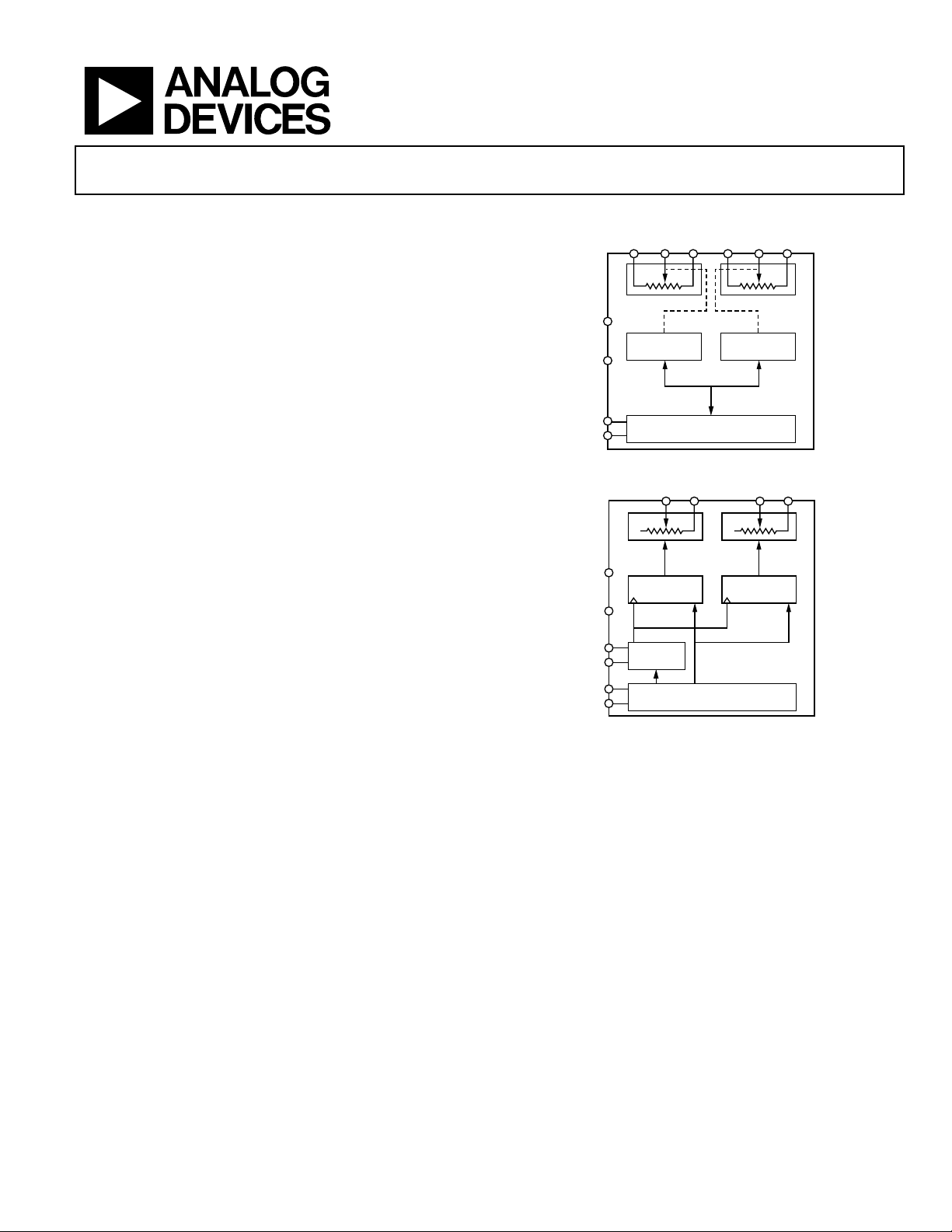
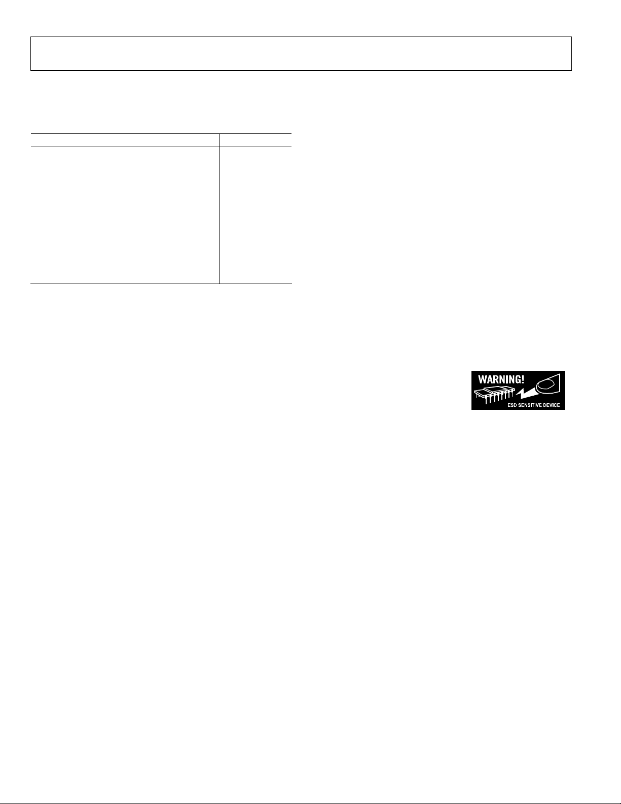
FUNCTIONAL BLOCK DIAGRAMS
W1
A1
V
DD
REGISTER 1
REGISTER 1
ADDRESS
DECODE
SDA
SCL
V
AD0
AD1
SDA
SCL
ND
DD
ND
Operating from a 2.7 V to 5.5 V power supply and consuming
less than 6 µA allows for usage in portable battery-operated
applications.
For applications that program the AD5243/AD5258 at the
factory, Analog Devices offers device programming software
running on Windows® NT/2000/XP operating systems. This
software effectively replaces any external I
in turn enhances users’ systems time-to-market. An AD5243/
AD5248 evaluation kit and software are available. The kit
includes a cable and instruction manual.
1The terms digital potentiometer, VR, and RDAC are used interchangeably.
B1 A2 W2
WIPER
PC INTERFACE
Figure 1. AD5243
W1
B1 W2
RDAC
/
8
SERIAL INPUT
REGISTER
Figure 2. AD5248
B2
WIPER
REGISTER 2
AD5243
B2
RDAC
REGISTER 2
AD5248
2
C controllers, which
04109-0-001
04109-0-002
Rev. 0
Information furnished by Analog Devices is believed to be accurate and reliable.
However, no responsibility is assumed by Analog Devices for its use, nor for any
infringements of patents or other rights of third parties that may result from its use.
Specifications subject to change without notice. No license is granted by implication
or otherwise under any patent or patent rights of Analog Devices. Trademarks and
registered trademarks are the property of their respective owners.
One Technology Way, P.O. Box 9106, Norwood, MA 02062-9106, U.S.A.
Tel: 781.329.4700
Fax: 781.326.8703 © 2004 Analog Devices, Inc. All rights reserved.
www.analog.com
Page 2

AD5243/AD5248
TABLE OF CONTENTS
Electrical Characteristics—2.5 kΩ Version ................................... 3
ESD Protection ........................................................................... 14
Electrical Characteristics—10 kΩ, 50 kΩ, 100 kΩ Versions ....... 4
Timing Characteristics—All Versions ........................................... 5
Absolute Maximum Ratings............................................................ 6
ESD Caution.................................................................................. 6
Pin Configurations and Function Descriptions ........................... 7
Typical Performance Characteristics ............................................. 8
Tes t Ci rc u it s ..................................................................................... 12
Theory of Operation ...................................................................... 13
Pro g ra m min g th e Var iab l e R e si s tor a nd Volt a ge .................... 13
Programming the Potentiometer Divider............................... 14
REVISION HISTORY
Revision 0: Initial Version
Terminal Voltage Operating Range.......................................... 14
Power-Up Sequence ................................................................... 14
Layout and Power Supply Bypassing ....................................... 14
Constant Bias to Retain Resistance Setting............................. 15
Evaluation Board ........................................................................ 15
2
I
C Interface .................................................................................... 16
2
I
C Compatible 2-Wire Serial Bus ........................................... 16
Outline Dimensions....................................................................... 19
Ordering Guide .......................................................................... 19
Rev. 0 | Page 2 of 20
Page 3

AD5243/AD5248
ELECTRICAL CHARACTERISTICS—2.5 kΩ VERSION
VDD = 5 V ± 10%, or 3 V ± 10%; VA = +VDD; VB = 0 V; −40°C < TA < +125°C; unless otherwise noted.
Table 1.
Parameter Symbol Conditions Min Typ
DC CHARACTERISTICS—RHEOSTAT MODE
Resistor Differential Nonlinearity
Resistor Integral Nonlinearity
Nominal Resistor Tolerance
2
2
3
R-DNL RWB, VA = no connect −2 ±0.1 +2 LSB
R-INL RWB, VA = no connect −6 ±0.75 +6 LSB
∆R
AB
TA = 25°C −20 +55 %
Resistance Temperature Coefficient (∆RAB/RAB )/∆T VAB = VDD, wiper = no connect 35 ppm/°C
RWB (Wiper Resistance) R
WB
Code = 0x00, VDD = 5 V 160 200 Ω
DC CHARACTERISTICS—POTENTIOMETER DIVIDER MODE (Specifications Apply to All VRs)
Differential Nonlinearity
4
DNL −1.5 ±0.1 +1.5 LSB
Integral Nonlinearity INL −2 ±0.6 +2 LSB
Voltage Divider Temperature
(∆V
)/∆T Code = 0x80 15 ppm/°C
W/VW
Coefficient
Full-Scale Error V
Zero-Scale Error V
WFSE
WZSE
Code = 0xFF −10 −2.5 0 LSB
Code = 0x00 0 2 10 LSB
RESISTOR TERMINALS
Voltage Range
Capacitance6 A, B C
Capacitance6 W C
Shutdown Supply Current
Common-Mode Leakage I
5
7
VA, VB, V
A, CB
W
I
A_SD
CM
W
GND V
f = 1 MHz, measured to GND, Code = 0x80
f = 1 MHz, measured to GND, Code = 0x80
45 pF
60 pF
VDD = 5.5 V 0.01 1 µA
VA = VB = VDD/2 1 nA
DIGITAL INPUTS AND OUTPUTS
Input Logic High V
Input Logic Low V
Input Logic High V
Input Logic Low V
Input Current I
Input Capacitance
6
IH
IL
IH
IL
IL
C
IL
VDD = 5 V 2.4 V
VDD = 5 V 0.8 V
VDD = 3 V 2.1 V
VDD = 3 V 0.6 V
VIN = 0 V or 5 V ±1 µA
5 pF
POWER SUPPLIES
Power Supply Range V
Supply Current I
Power Dissipation
8
DD RANGE
DD
P
DISS
2.7 5.5 V
VIH = 5 V or VIL = 0 V 3.5 6 µA
VIH = 5 V or VIL = 0 V, VDD = 5 V 30 µW
Power Supply Sensitivity PSS VDD = 5 V ± 10%, Code = midscale ±0.02 ±0.08 %/%
DYNAMIC CHARACTERISTICS
9
Bandwidth −3 dB BW_2.5 K Code = 0x80 4.8 MHz
Total Harmonic Distortion THD
VW Settling Time t
Resistor Noise Voltage Density e
See notes at end of section.
W
S
N_WB
VA = 1 V rms, VB = 0 V, f = 1 kHz 0.1 %
VA = 5 V, VB = 0 V, ±1 LSB error band 1 µs
RWB = 1.25 kΩ, RS = 0 3.2
1
Max Unit
DD
V
nV/√Hz
Rev. 0 | Page 3 of 20
Page 4

AD5243/AD5248
ELECTRICAL CHARACTERISTICS—10 kΩ, 50 kΩ, 100 kΩ VERSIONS
VDD = 5 V ± 10%, or 3 V ± 10%; VA = VDD; VB = 0 V; −40°C < TA < 125°C; unless otherwise noted.
Table 2.
Parameter Symbol Conditions Min Typ
DC CHARACTERISTICS—RHEOSTAT MODE
Resistor Differential Nonlinearity
Resistor Integral Nonlinearity
Nominal Resistor Tolerance
2
2
3
R-DNL RWB, VA = no connect −1 ±0.1 +1 LSB
R-INL RWB, VA = no connect −2.5 ±0.25 +2.5 LSB
∆R
AB
TA = 25°C −20 +20 %
Resistance Temperature Coefficient (∆RAB/RAB )/∆T VAB = VDD, wiper = no connect 35 ppm/°C
RWB (Wiper Resistance) R
WB
Code = 0x00, VDD =5 V 160 200 Ω
DC CHARACTERISTICS—POTENTIOMETER DIVIDER MODE (Specifications Apply to All VRs)
Differential Nonlinearity
Integral Nonlinearity
Voltage Divider Temperature
4
4
DNL −1 ±0.1 +1 LSB
INL −1 ±0.3 +1 LSB
(∆V
)/∆T Code = 0x80 15 ppm/°C
W/VW
Coefficient
Full-Scale Error V
Zero-Scale Error V
WFSE
WZSE
Code = 0xFF −2.5 −1 0 LSB
Code = 0x00 0 1 2.5 LSB
RESISTOR TERMINALS
Voltage Range
Capacitance6 A, B C
Capacitance6 W C
Shutdown Supply Current
Common-Mode Leakage I
5
7
VA, VB, V
A, CB
W
I
A_SD
CM
W
GND V
f = 1 MHz, measured to GND, Code = 0x80
f = 1 MHz, measured to GND, Code = 0x80
45 pF
60 pF
VDD = 5.5 V 0.01 1 µA
VA = VB = VDD/2 1 nA
DIGITAL INPUTS AND OUTPUTS
Input Logic High V
Input Logic Low V
Input Logic High V
Input Logic Low V
Input Current I
Input Capacitance C
IH
IL
IH
IL
IL
IL
VDD = 5 V 2.4 V
VDD = 5 V 0.8 V
VDD = 3 V 2.1 V
VDD = 3 V 0.6 V
VIN = 0 V or 5 V ±1 µA
5 pF
POWER SUPPLIES
Power Supply Range V
Supply Current I
Power Dissipation P
DD RANGE
DD
DISS
2.7 5.5 V
VIH = 5 V or VIL = 0 V 3.5 6 µA
VIH = 5 V or VIL = 0 V, VDD = 5 V 30 µW
Power Supply Sensitivity PSS VDD = 5 V ± 10%, Code = midscale ±0.02
DYNAMIC CHARACTERISTICS
Bandwidth −3 dB BW
Total Harmonic Distortion THD
VW Settling Time (10 kΩ/50 kΩ/100
t
S
W
RAB = 10 kΩ/50 kΩ/100 kΩ, Code = 0x80
VA = 1 V rms, VB = 0 V, f = 1 kHz, RAB = 10 kΩ
0.1 %
VA = 5 V, VB = 0 V, ±1 LSB error band 2 µs
kΩ)
Resistor Noise Voltage Density e
See notes at end of section.
N_WB
RWB = 5 kΩ, RS = 0 9
1
600/100/4
0
Max Unit
V
DD
±0.0
%/%
8
kHz
nV/√Hz
Rev. 0 | Page 4 of 20
Page 5

AD5243/AD5248
TIMING CHARACTERISTICS—ALL VERSIONS
VDD = 5V ± 10%, or 3V ± 10%; VA = VDD; VB = 0 V; −40°C < TA < +125°C; unless otherwise noted.
Table 3.
Parameter Symbol Conditions Min Typ1 Max Unit
I2C INTERFACE TIMING CHARACTERISTICS
SCL Clock Frequency f
t
Bus Free Time between STOP and START t
BUF
t
Hold Time (Repeated START) t
HD;STA
t
Low Period of SCL Clock t
LOW
t
High Period of SCL Clock t
HIGH
t
Setup Time for Repeated START Condition t
SU;STA
t
Data Hold Time
HD;DAT
t
Data Setup Time t
SU;DAT
11
tF Fall Time of Both SDA and SCL Signals t
tR Rise Time of Both SDA and SCL Signals t
t
Setup Time for STOP Condition t
SU;STO
See notes at end of section.
NOTES
1
Typical specifications represent average readings at 25°C and VDD = 5 V.
2
Resistor position nonlinearity error R-INL is the deviation from an ideal value measured between the maximum resistance and the minimum resistance wiper
positions. R-DNL measures the relative step change from ideal between successive tap positions. Parts are guaranteed monotonic.
3
VAB = VDD, wiper (VW) = no connect.
4
INL and DNL are measured at VW with the RDAC configured as a potentiometer divider similar to a voltage output D/A converter. VA = VDD and VB = 0 V.
DNL specification limits of ±1 LSB maximum are guaranteed monotonic operating conditions.
5
Resistor terminals A, B, W have no limitations on polarity with respect to each other.
6
Guaranteed by design and not subject to production test.
7
Measured at the A terminal. The A terminal is open circuited in shutdown mode.
8
P
is calculated from (IDD × VDD). CMOS logic level inputs result in minimum power dissipation.
DISS
9
All dynamic characteristics use VDD = 5 V.
10
See timing diagrams for locations of measured values.
11
The maximum t
must be met only if the device does not stretch the low period (t
HD:DAT
10
(Specifications Apply to All Parts)
SCL
1
2
0 400 kHz
1.3 µs
After this period, the first clock pulse is
generated.
3
4
5
t
6
7
8
9
10
1.3 µs
0.6 µs
0.6 µs
0.9 µs
100 ns
300 ns
300 ns
0.6 µs
) of the SCL signal.
LOW
0.6 µs
Rev. 0 | Page 5 of 20
Page 6
AD5243/AD5248
ABSOLUTE MAXIMUM RATINGS
TA = 25°C, unless otherwise noted.
Table 4.
Parameter Value
VDD to GND –0.3 V to +7 V
VA, VB, VW to GND V
Terminal Current, Ax to Bx, Ax to Wx, Bx to Wx1
Pulsed ±20 mA
Continuous ±5 mA
Digital Inputs and Output Voltage to GND 0 V to 7 V
Operating Temperature Range –40°C to +125°C
Maximum Junction Temperature (T
) 150°C
JMAX
Storage Temperature –65°C to +150°C
Lead Temperature (Soldering, 10 sec) 300°C
Thermal Resistance2 θJA: MSOP-10
1
Maximum terminal current is bounded by the maximum current handling of
the switches, maximum power dissipation of the package, and maximum
applied voltage across any two of the A, B, and W terminals at a given
resistance.
2
Package power dissipation = (T
− TA)/θJA.
JMAX
DD
230°C/W
Stresses above those listed under Absolute Maximum Ratings
may cause permanent damage to the device. This is a stress
rating only; functional operation of the device at these or any
other conditions above those indicated in the operational
section of this specification is not implied. Exposure to absolute
maximum rating conditions for extended periods may affect
device reliability.
ESD CAUTION
ESD (electrostatic discharge) sensitive device. Electrostatic charges as high as 4000 V readily accumulate on
the human body and test equipment and can discharge without detection. Although this product features
proprietary ESD protection circuitry, permanent damage may occur on devices subjected to high energy
electrostatic discharges. Therefore, proper ESD precautions are recommended to avoid performance
degradation or loss of functionality.
Rev. 0 | Page 6 of 20
Page 7

AD5243/AD5248
PIN CONFIGURATIONS AND FUNCTION DESCRIPTIONS
W2
1
B1
2
A1
3
AD5243
TOP VIEW
4
5
DD
10
W1
9
B2
8
A2
7
SDAGND
6
SCLV
04109-0-027
Figure 3. AD5243 Pin Configuration
Table 5. AD5243 Pin Function Descriptions
Pin
No.
Mnemonic Description
1 B1 B1 Terminal.
2 A1 A1 Terminal.
3 W2 W2 Terminal.
4 GND Digital Ground.
5 V
DD
6 SCL
Positive Power Supply.
Serial Clock Input. Positive edge
triggered.
7 SDA Serial Data Input/Output.
8 A2 A2 Terminal.
9 B2 B2 Terminal.
10 W1 W1 Terminal.
AD0
W2
1
B1
2
3
AD5248
TOP VIEW
4
5
DD
10
W1
9
B2
8
AD1
7
SDAGND
6
SCLV
04109-0-028
Figure 4. AD5248 Pin Configuration
Table 6. AD5248 Pin Function Descriptions
Pin
No.
Mnemonic Description
1 B1 B1 Terminal.
2 AD0
Programmable Address Bit 0 for Multiple
Package Decoding.
3 W2 W2 Terminal.
4 GND Digital Ground.
5 V
DD
6 SCL
Positive Power Supply.
Serial Clock Input. Positive edge
triggered.
7 SDA Serial Data Input/Output.
8 AD1
Programmable Address Bit 1 for Multiple
Package Decoding.
9 B2 B2 Terminal.
10 W1 W1 Terminal.
Rev. 0 | Page 7 of 20
Page 8

AD5243/AD5248
TYPICAL PERFORMANCE CHARACTERISTICS
2.0
1.5
1.0
0.5
0
–0.5
–1.0
RHEOSTAT MODE INL (LSB)
–1.5
–2.0
VDD = 2.7V
Figure 5. R-INL vs. Code vs. Supply Voltages
0.5
0.4
0.3
0.2
0.1
0
–0.1
–0.2
RHEOSTAT MODE DNL (LSB)
–0.3
–0.4
–0.5
Figure 6. R-DNL vs. Code vs. Supply Voltages
0.5
0.4
0.3
0.2
0.1
0
–0.1
–0.2
–0.3
POTENTIOMETER MODE INL (LSB)
–0.4
–0.5
Figure 7. INL vs. Code vs. Temperature
VDD = 5.5V
1289632 640 160 192 224 256
CODE (DECIMAL)
VDD = 2.7V
VDD = 5.5V
1289632 640 160 192 224 256
CODE (DECIMAL)
VDD = 5.5V
T
= –40°C, +25°C, +85°C, +125°C
A
VDD = 2.7V
T
= –40°C, +25°C, +85°C, +125°C
A
1289632 640 160 192 224 256
CODE (DECIMAL)
TA = 25°C
= 10kΩ
R
AB
TA = 25°C
R
= 10kΩ
AB
RAB = 10kΩ
04109-0-030
04109-0-031
04109-0-032
0.5
0.4
0.3
0.2
0.1
0
–0.1
–0.2
–0.3
POTENTIOMETER MODE DNL (LSB)
–0.4
–0.5
VDD = 2.7V; TA = –40°C, +25°C, +85°C, +125°C
1289632 640 160 192 224 256
CODE (DECIMAL)
RAB = 10kΩ
04109-0-033
Figure 8. DNL vs. Code vs. Temperature
1.0
0.8
0.6
0.4
0.2
0
–0.2
–0.4
–0.6
POTENTIOMETER MODE INL (LSB)
–0.8
–1.0
VDD = 2.7V
1289632 640 160 192 224 256
CODE (DECIMAL)
VDD = 5.5V
TA = 25°C
R
= 10kΩ
AB
04109-0-034
Figure 9. INL vs. Code vs. Supply Voltages
0.5
0.4
0.3
0.2
0.1
0
–0.1
–0.2
–0.3
POTENTIOMETER MODE DNL (LSB)
–0.4
–0.5
VDD = 2.7V
VDD = 5.5V
1289632 640 160 192 224 256
CODE (DECIMAL)
TA = 25°C
R
= 10kΩ
AB
04109-0-035
Figure 10. DNL vs. Code vs. Supply Voltages
Rev. 0 | Page 8 of 20
Page 9

AD5243/AD5248
2.0
VDD = 2.7V
1.5
TA = –40°C, +25°C, +85°C, +125°C
1.0
0.5
RAB = 10kΩ
4.50
RAB = 10kΩ
3.75
3.00
0
–0.5
–1.0
RHEOSTAT MODE INL (LSB)
–1.5
–2.0
Figure 11. R-INL vs. Code vs. Temperature
0.5
0.4
0.3
0.2
0.1
–0.1
–0.2
RHEOSTAT MODE DNL (LSB)
–0.3
–0.4
–0.5
VDD = 2.7V, 5.5V; TA = –40°C, +25°C, +85°C, +125°C
0
Figure 12. R-DNL vs. Code vs. Temperature
2.0
1.5
1.0
0.5
0
–0.5
–1.0
FSE, FULL-SCALE ERROR (LSB)
–1.5
VDD = 2.7V, VA = 2.7V
VDD = 5.5V
T
= –40°C, +25°C, +85°C, +125°C
A
1289632 640 160 192 224 256
CODE (DECIMAL)
1289632 640 160 192 224 256
CODE (DECIMAL)
VDD = 5.5V, VA = 5.0V
RAB = 10kΩ
RAB = 10kΩ
04109-0-036
04109-0-037
2.25
1.50
ZSE, ZERO-SCALE ERROR (LSB)
0.75
VDD = 2.7V, VA = 2.7V
VDD = 5.5V, VA = 5.0V
0
–40 –25 –10 5 20 35 50 65 80 95 110 125
TEMPERATURE (°C)
Figure 14. Zero-Scale Error vs. Temperature
10
A)
µ
1
, SUPPLY CURRENT (
DD
I
0.1
–40 –7 26 59 92 125
VDD = 5V
VDD = 3V
TEMPERATURE (°C)
Figure 15. Supply Current vs. Temperature
120
100
80
60
40
20
RHEOSTAT MODE TEMPCO (ppm/°C)
0
VDD = 2.7V
TA = –40°C TO +85°C, –40°C TO +125°C
VDD = 5.5V
T
= –40°C TO +85°C, –40°C TO +125°C
A
RAB = 10kΩ
04109-0-039
04109-0-040
–2.0
–40 –25 –10 5 20 35 50 65 80 95 110 125
TEMPERATURE (°C)
Figure 13. Full-Scale Error vs. Temperature
04109-0-038
Rev. 0 | Page 9 of 20
–20
CODE (DECIMAL)
Figure 16. Rheostat Mode Tempco ∆R
1289632 640 160 192 224 256
/∆T vs. Code
WB
04109-0-041
Page 10

AD5243/AD5248
50
40
30
VDD = 2.7V
T
20
10
0
–10
–20
POTENTIOMETER MODE TEMPCO (ppm/°C)
–30
Figure 17. Potentiometer Mode Tempco ∆V
0
–6
–12
–18
–24
–30
GAIN (dB)
–36
–42
–48
–54
–60
10k 1M100k 10M
0
–6
–12
–18
–24
–30
GAIN (dB)
–36
–42
–48
–54
–60
1k 100k10k 1M
= –40°C TO +85°C, –40°C TO +125°C
A
VDD = 5.5V
T
= –40°C TO +85°C, –40°C TO +125°C
A
1289632 640 160 192 224 256
CODE (DECIMAL)
0x80
0x40
0x20
0x10
0x08
0x04
0x010x02
FREQUENCY (Hz)
Figure 18. Gain vs. Frequency vs. Code, R
0x80
0x40
0x20
0x10
0x08
0x04
0x02
0x01
FREQUENCY (Hz)
Figure 19. Gain vs. Frequency vs. Code, R
RAB = 10kΩ
/∆T vs. Code
WB
= 2.5 kΩ
AB
= 10 kΩ
AB
0
0x80
0x40
0x20
0x10
0x08
0x04
0x02
0x01
FREQUENCY (Hz)
= 50 kΩ
AB
04109-0-045
04109-0-042
–6
–12
–18
–24
–30
GAIN (dB)
–36
–42
–48
–54
–60
1k 100k10k 1M
Figure 20. Gain vs. Frequency vs. Code, R
0
0x80
0x40
0x20
0x10
0x08
0x04
0x02
0x01
FREQUENCY (Hz)
= 100 kΩ
AB
04109-0-046
04109-0-043
–6
–12
–18
–24
–30
GAIN (dB)
–36
–42
–48
–54
–60
1k 100k10k 1M
Figure 21. Gain vs. Frequency vs. Code, R
0
–6
–12
–18
–24
–30
GAIN (dB)
–36
–42
–48
–54
–60
04109-0-044
100kΩ
60kHz
50kΩ
120kHz
10kΩ
570kHz
2.5kΩ
2.2MHz
10k1k 100k 1M 10M
FREQUENCY (Hz)
Figure 22. –3 dB Bandwidth @ Code = 0x80
04109-0-047
Rev. 0 | Page 10 of 20
Page 11

AD5243/AD5248
10
TA = 25°C
1
0.1
, SUPPLY CURRENT (mA)
DD
I
0.01
0 0.5 1.0 1.5 2.0 2.5 3.0 3.5 4.0 4.5 5.0
VDD = 2.7V
DIGITAL INPUT VOLTAGE (V)
Figure 23. I
VDD = 5.5V
vs. Input Voltage
DD
V
W
SCL
04109-0-052
V
W2
V
W1
04109-0-051
Figure 26. Analog Crosstalk
V
W
04109-0-053
04109-0-048
Figure 24. Digital Feedthrough
V
W2
V
W1
04109-0-049
V
SCL
Figure 25. Digital Crosstalk
Figure 27. Midscale Glitch, Code 0x80 to 0x7F
W
Figure 28. Large Signal Settling Time
04109-0-050
Rev. 0 | Page 11 of 20
Page 12

AD5243/AD5248
V
TEST CIRCUITS
Figure 29 through Figure 35 illustrate the test circuits that define the test conditions used in the product specification tables.
V+ = V
DUT
A
V+
W
B
DD
1LSB = V+/2
V
MS
N
04109-0-003
OFFSET
GND
V
IN
2.5V
DUT
A
W
B
+15V
AD8610
–15V
V
OUT
04109-0-009
Figure 29. Test Circuit for Potentiometer Divider Nonlinearity Error
(INL, DNL)
NO CONNECT
DUT
A
W
B
I
W
V
MS
04109-0-004
Figure 30. Test Circuit for Resistor Position Nonlinearity Error
(Rheostat Operation; R-INL, R-DNL)
MS2
DUT
A
W
B
V
W
V
IW = VDD/R
MS1
RW = [V
NOMINAL
MS1
– V
MS2
]/I
W
04109-0-005
Figure 31. Test Circuit for Wiper Resistance
V
A
DUT
A
∆V
DD
V+
W
B
V+ = VDD± 10%
PSRR (dB) = 20 LOG
PSS (%/%) =
V
MS
∆VMS%
∆VDD%
∆V
MS
( )
∆V
DD
04109-0-006
Figure 33. Test Circuit for Gain vs. Frequency
0.1V
RSW=
I
CODE = 0x00
TO V
V
SS
DD
SW
0.1V
04109-0-010
B
DUT
W
I
SW
Figure 34. Test Circuit for Incremental On Resistance
NC
DUT
GND
NC
A
W
B
V
DD
I
CM
NC = NO CONNECT
V
CM
04109-0-011
Figure 35. Test Circuit for Common-Mode Leakage Current
Figure 32. Test Circuit for Power Supply Sensitivity(PSS, PSSR)
Rev. 0 | Page 12 of 20
Page 13

AD5243/AD5248
−
THEORY OF OPERATION
The AD5243/AD5248 are 256-position digitally controlled
variable resistor (VR) devices.
The general equation determining the digitally programmed
output resistance between W and B is
An internal power-on preset places the wiper at midscale
during power-on, which simplifies the fault condition recovery
at power-up.
PROGRAMMING THE VARIABLE RESISTOR AND VOLTAGE
Rheostat Operation
The nominal resistance of the RDAC between Terminals A and
B is available in 2.5 kΩ, 10 kΩ, 50 kΩ, and 100 kΩ. The nominal
resistance (R
the wiper terminal, plus the B terminal contact. The 8-bit data
in the RDAC latch is decoded to select one of the 256 possible
settings.
Assuming that a 10 kΩ part is used, the wiper’s first connection
starts at the B terminal for data 0x00. Because there is a 50 Ω
wiper contact resistance, such a connection yields a minimum
of 100 Ω (2 × 50 Ω) resistance between Terminals W and B. The
second connection is the first tap point, which corresponds to
139 Ω (R
0x01. The third connection is the next tap point, representing
178 Ω (2 × 39 Ω + 2 × 50 Ω) for data 0x02, and so on. Each LSB
data value increase moves the wiper up the resistor ladder until
the last tap point is reached at 10,100 Ω (R
) of the VR has 256 contact points accessed by
AB
A
W
B
Figure 36. Rheostat Mode Configuration
= RAB/256 + 2 × RW = 39 Ω + 2 × 50 Ω) for data
WB
A
W
B
R
S
A
W
B
+ 2 × RW).
AB
A
04109-0-012
WB
256
D
DR ×+×= 2
)(
AB
(1)
RR
W
where:
D is the decimal equivalent of the binary code loaded in the
8-bit RDAC register.
is the end-to-end resistance.
R
AB
R
is the wiper resistance contributed by the on resistance of
W
the internal switch.
In summary, if R
circuited, the following output resistance R
= 10 kΩ and the A terminal is open
AB
is set for the
WB
indicated RDAC latch codes.
Table 7. Codes and Corresponding R
Resistance
WB
D (Dec) RWB (Ω) Output State
255 9,961 Full scale (RAB − 1 LSB + RW)
128 5,060 Midscale
1 139 1 LSB
0 100 Zero scale (wiper contact resistance)
Note that, in the zero-scale condition, a finite wiper resistance
of 100 Ω is present. Care should be taken to limit the current
flow between W and B in this state to a maximum pulse current
of no more than 20 mA. Otherwise, degradation or possible
destruction of the internal switch contact can occur.
Similar to the mechanical potentiometer, the resistance of the
RDAC between the Wiper W and Terminal A also produces a
digitally controlled complementary resistance, R
. When these
WA
terminals are used, the B terminal can be opened. Setting the
resistance value for R
starts at a maximum value of resistance
WA
and decreases as the data loaded in the latch increases in value.
The general equation for this operation is
D
D7
D6
D5
D4
D3
D2
D1
D0
R
S
R
S
W
= 10 kΩ and the B terminal open circuited, the
For R
AB
following output resistance R
256
DR ×+×
= 2
)(
256
(2)
RR
ABWA
W
is set for the indicated RDAC
WA
latch codes.
Table 8. Codes and Corresponding R
Resistance
WA
D (Dec) RWA (Ω) Output State
RDAC
LATCH
AND
DECODER
R
S
B
255 139 Full scale
128 5,060 Midscale
1 9,961 1 LSB
0 10,060 Zero scale
04109-0-013
Figure 37. AD5243 Equivalent RDAC Circuit
Rev. 0 | Page 13 of 20
Page 14

AD5243/AD5248
Typical device-to-device matching is process lot dependent and
may vary by up to ±30%. Because the resistance element is
processed in thin film technology, the change in R
AB
with
temperature has a very low 35 ppm/°C temperature coefficient.
PROGRAMMING THE POTENTIOMETER DIVIDER
Voltage Output Operation
The digital potentiometer easily generates a voltage divider at
wiper-to-B and wiper-to-A proportional to the input voltage at
A to B. Unlike the polarity of V
positive, voltage across A to B, W to A, and W to B can be at
either polarity.
V
I
Figure 38. Potentiometer Mode Configuration
If ignoring the effect of the wiper resistance for approximation,
connecting the A terminal to 5 V and the B terminal to ground
produces an output voltage at the wiper-to-B starting at 0 V up
to 1 LSB less than 5 V. Each LSB of voltage is equal to the voltage applied across terminal AB divided by the 256 positions of
the potentiometer divider. The general equation defining the
output voltage at V
with respect to ground for any valid input
W
voltage applied to terminals A and B is
W
256
D
DV
)(
256
V
+=
A
A more accurate calculation, which includes the effect of wiper
resistance, V
, is
W
DR
)(
WB
DV
)(
W
V
A
R
AB
Operation of the digital potentiometer in the divider mode
results in a more accurate operation overtemperature. Unlike
the rheostat mode, the output voltage is dependent mainly on
the ratio of the internal resistors R
absolute values. Therefore, the temperature drift reduces to
15 ppm/°C.
to GND, which must be
DD
A
W
V
O
B
D
−
(3)
V
B
256
DR
)(
WA
+=
R
(4)
V
B
AB
and RWB and not the
WA
04109-0-014
340Ω
LOGIC
GND
Figure 39. ESD Protection of Digital Pins
A, B, W
GND
Figure 40. ESD Protection of Resistor Terminals
04109-0-015
04109-0-016
TERMINAL VOLTAGE OPERATING RANGE
The AD5243/AD5248 VDD and GND power supply defines the
boundary conditions for proper 3-terminal digital potentiometer operation. Supply signals present on Terminals A, B, and W
that exceed V
or GND are clamped by the internal forward
DD
biased diodes (see Figure 41).
V
DD
A
W
B
GND
04109-0-017
Figure 41. Maximum Terminal Voltages Set by V
and GND
DD
POWER-UP SEQUENCE
Because the ESD protection diodes limit the voltage compliance
at Terminals A, B, and W (see Figure 41), it is important to
power V
and W; otherwise, the diode is forward biased such that V
/GND before applying any voltage to Terminals A, B,
DD
DD
is
powered unintentionally and may affect the rest of the user’s
circuit. The ideal power-up sequence is in the following order:
GND, V
order of powering V
important as long as they are powered after V
, digital inputs, and then VA, VB, and VW. The relative
DD
, VB, VW, and the digital inputs is not
A
/GND.
DD
LAYOUT AND POWER SUPPLY BYPASSING
It is good practice to employ compact, minimum lead length
layout design. The leads to the inputs should be as direct as
possible with a minimum conductor length. Ground paths
should have low resistance and low inductance.
ESD PROTECTION
All digital inputs are protected with a series of input resistors
and parallel Zener ESD structures, shown in Figure 39 and
Figure 40. This applies to the digital input pins SDA, SCL, AD0,
and AD1 (AD5248 only).
Rev. 0 | Page 14 of 20
Similarly, it is also good practice to bypass the power supplies
with quality capacitors for optimum stability. Supply leads to the
device should be bypassed with disk or chip ceramic capacitors
of 0.01 µF to 0.1 µF. Low ESR 1 µF to 10 µF tantalum or electrolytic capacitors should also be applied at the supplies to
minimize any transient disturbance and low frequency ripple
(see Figure 42). Note that the digital ground should also be
joined remotely to the analog ground at one point to minimize
the ground bounce.
Page 15

AD5243/AD5248
This demonstrates that constantly biasing the potentiometer is
V
DD
+
C3
10µFC10.1µF
Figure 42. Power Supply Bypassing
V
DD
AD5243
GND
04109-0-018
CONSTANT BIAS TO RETAIN RESISTANCE SETTING
For users who desire nonvolatility but cannot justify the additional cost for the EEMEM, the AD5243/AD5248 may be
considered as low cost alternatives by maintaining a constant
bias to retain the wiper setting. The AD5243/AD5248 are
designed specifically with low power in mind, which allows low
power consumption even in battery-operated systems. The
graph in Figure 43 demonstrates the power consumption from a
3.4 V 450 mAhr Li-Ion cell phone battery, which is connected to
the AD5243/AD5248. The measurement over time shows that
the device draws approximately 1.3 µA and consumes negligible
power. Over a course of 30 days, the battery is depleted by less
than 2%, the majority of which is due to the intrinsic leakage
current of the battery itself.
110%
108%
106%
104%
102%
100%
98%
96%
BATTERY LIFE DEPLETED
94%
92%
90%
0
51015
Figure 43. Battery Operating Life Depletion
DAYS
TA= 25
°C
20 25 30
04109-0-019
not an impractical approach. Most portable devices do not
require the removal of batteries for the purpose of charging.
Although the resistance setting of the AD5243/AD5248 is lost
when the battery needs replacement, such events occur rather
infrequently such that this inconvenience is justified by the
lower cost and smaller size offered by the AD5243/AD5248. If
and when total power is lost, the user should be provided with a
means to adjust the setting accordingly.
EVALUATION BOARD
An evaluation board, along with all necessary software, is available to program the AD5243/AD5248 from any PC running
Windows 98/2000/XP. The graphical user interface, as shown in
Figure 44, is straightforward and easy to use. More detailed
information is available in the user manual, which comes with
the board.
Figure 44. AD5243 Evaluation Board Software
The AD5243/AD5248 start at midscale upon power-up. To
increment or decrement the resistance, the user may simply
move the scrollbars on the left. To write any specific value, the
user should use the bit pattern in the upper screen and press the
Run button. The format of writing data to the device is shown
in Table 9. To read the data out from the device, the user can
simply press the Read button. The format of the read bits is
shown in Table 10.
Rev. 0 | Page 15 of 20
Page 16

AD5243/AD5248
I2C INTERFACE
I2C COMPATIBLE 2-WIRE SERIAL BUS
The 2-wire I2C serial bus protocol operates as follows:
1. The master initiates data transfer by establishing a START
condition, which is when a high-to-low transition on the
SDA line occurs while SCL is high (see Figure 46). The
following byte is the slave address byte, which consists of
the slave address followed by an R/
mines whether data is read from or written to the slave
device). The AD5243 has a fixed slave address byte, while
the AD5248 has two configurable address bits AD0 and
AD1 (see Table 9).
The slave whose address corresponds to the transmitted
address responds by pulling the SDA line low during the
ninth clock pulse (this is termed the acknowledge bit). At
this stage, all other devices on the bus remain idle while the
selected device waits for data to be written to or read from
its serial register. If the R/
from the slave device. On the other hand, if the R/
low, the master writes to the slave device.
2. In the write mode, the second byte is the instruction byte.
The first bit (MSB) of the instruction byte is the RDAC
subaddress select bit. A Logic Low selects Channel 1 and a
Logic High selects Channel 2.
The second MSB, SD, is a shutdown bit. A logic high causes
an open circuit at Terminal A while shorting the wiper to
Terminal B. This operation yields almost 0 Ω in rheostat
mode or 0 V in potentiometer mode. It is important to note
that the shutdown operation does not disturb the contents
of the register. When brought out of shutdown, the previous setting is applied to the RDAC. Also, during shutdown,
new settings can be programmed. When the part is
returned from shutdown, the corresponding VR setting is
applied to the RDAC.
The remainder of the bits in the instruction byte are don’t
care bits (see Table 9).
After acknowledging the instruction byte, the last byte in
write mode is the data byte. Data is transmitted over the
serial bus in sequences of nine clock pulses (eight data bits
followed by an acknowledge bit). The transitions on the
SDA line must occur during the low period of SCL and
remain stable during the high period of SCL (see Figure 46
and Figure 47).
bit is high, the master reads
W
bit (this bit deter-
W
W
bit is
3. In the read mode, the data byte follows immediately after
the acknowledgment of the slave address byte. Data is
transmitted over the serial bus in sequences of nine clock
pulses (a slight difference with the write mode, eight data
bits are followed by an acknowledge bit). Similarly, the
transitions on the SDA line must occur during the low
period of SCL and remain stable during the high period of
SCL (see Figure 48 and Figure 49).
Note that the channel of interest is the one that is previously selected in the write mode. In the case where users
need to read the RDAC values of both channels, they need
to program the first channel in the write mode and then
change to the read mode to read the first channel value.
After that, they need to change back to the write mode with
the second channel selected and read the second channel
value in the read mode again. It is not necessary for users
to issue the Frame 3 data byte in the write mode for subsequent readback operation. Users should refer to Figure 48
and Figure 49 for the programming format.
4. After all data bits have been read or written, a STOP condi-
tion is established by the master. A STOP condition is
defined as a low-to-high transition on the SDA line while
SCL is hig h. In write mode, the master pulls the SDA line
high during the tenth clock pulse to establish a STOP
condition (see Figure 46 and Figure 47). In read mode, the
master issues a no acknowledge for the ninth clock pulse
(that is, the SDA line remains high). The master then
brings the SDA line low before the tenth clock pulse, which
goes high to establish a STOP condition (see Figure 48 and
Figure 49).
A repeated write function gives the user flexibility to
update the RDAC output a number of times after
addressing and instructing the part only once. For example,
after the RDAC has acknowledged its slave address and
instruction bytes in the write mode, the RDAC output
updates on each successive byte. If different instructions
are needed, the write/read mode has to start again with a
new slave address, instruction, and data byte. Similarly, a
repeated read function of the RDAC is also allowed.
Rev. 0 | Page 16 of 20
Page 17

AD5243/AD5248
Table 9. Write Mode
AD5243
S 0 1 0 1 1 1 1 W A A0 SD X X X X X X A D7 D6 D5 D4 D3 D2 D1 D0 A P
Slave Address Byte Instruction Byte Data Byte
AD5248
S 0 1 0 1 1 AD1 AD0 W A A0 SD X X X X X X A D7 D6 D5 D4 D3 D2 D1 D0 A P
Slave Address Byte Instruction Byte Data Byte
Table 10. Read Mode
AD5243
S 0 1 0 1 1 1 1 R A D7 D6 D5 D4 D3 D2 D1 D0 A P
Slave Address Byte Data Byte
AD5248
S 0 1 0 1 1 AD1 AD0 R A D7 D6 D5 D4 D3 D2 D1 D0 A P
Slave Address Byte Data Byte
LEGEND
S = Start condition.
P = Stop condition.
A = Acknowledge.
X = Don’t care.
W = Write.
AD0, AD1 = Package pin
programmable address bits.
R = Read.
A0 = RDAC subaddress select bit.
SD = Shutdown connects wiper to B terminal and
open circuits A terminal. It does not change contents
of wiper register.
D7, D6, D5, D4, D3, D2, D1, D0 = Data bits.
t
2
t
5
10
04109-0-021
P
SCL
SDA
t
t
1
PS
t
8
t
2
3
t
8
t
6
t
9
Figure 45. I
t
9
t
4
2
C Interface Detailed Timing Diagram
t
7
S
t
START BY
MASTER
SCL
SDA
1
01
01111
FRAME 1
SLAVE ADDRESS BYTE
19
R/W A0 SD X X X X
ACK BY
AD5243
X
X
FRAME 2
INSTRUCTION BYTE
Figure 46. Writing to the RDAC Register—AD5243
19
D7 D6 D5 D4 D3
ACK BY
AD5243
FRAME 3
DATA BYTE
D2 D1 D0
9
ACK BY
AD5243
STOP BY
MASTER
04109-0-022
Rev. 0 | Page 17 of 20
Page 18

AD5243/AD5248
START BY
MASTER
SCL
SDA
1
01
0 1 1 AD1 AD0
FRAME 1
SLAVE ADDRESS BYTE
R/W A0 SD X X X X
ACK BY
AD5248
19
X
X
FRAME 2
INSTRUCTION BYTE
19
D7 D6 D5 D4 D3
ACK BY
AD5248
FRAME 3
DATA BYTE
D2 D1 D0
9
ACK BY
AD5248
STOP BY
MASTER
04109-0-023
Figure 47. Writing to the RDAC Register—AD5248
START BY
MASTER
1
SCL
01
SDA
01111
FRAME 1
SLAVE ADDRESS BYTE
R/W D7 D6 D4 D3 D2 D1 D0
Figure 48. Reading Data from a Previously Selected RDAC Register in Write Mode—AD5243
ACK BY
AD5243
19
D5
FRAME 2
RDAC REGISTER
9
NO ACK
BY MASTER
STOP BY
MASTER
04109-0-024
199
D5
ACK BY
AD5248
FRAME 2
RDAC REGISTER
NO ACK
BY MASTER
STOP BY
MASTER
04109-0-025
START BY
MASTER
1
SCL
SDA
01
0 1 1 AD1 AD0
FRAME 1
SLAVE ADDRESS BYTE
R/W D7 D6 D4 D3 D2 D1 D0
Figure 49. Reading Data from a Previously Selected RDAC Register in Write Mode—AD5248
Multiple Devices on One Bus (Applies Only to AD5248)
Figure 50 shows four AD5248 devices on the same serial bus.
Each has a different slave address, because the states of their
AD0 and AD1 pins are different. This allows each device on the
bus to be written to or read from independently. The master
device output bus line drivers are open-drain pull-downs in a
2
C compatible interface.
fully I
MASTER
5V
R
PRP
SDA
AD1
AD0
AD5248
SCL
5V
SDA
AD1
AD0
AD5248
SCL
5V
SDA
AD1
AD0
AD5248
Figure 50. Multiple AD5248 Devices on One I
SCL
2
C Bus
5V
SDA
AD1
AD0
AD5248
SCL
SDA
SCL
04109-0-026
Rev. 0 | Page 18 of 20
Page 19

AD5243/AD5248
OUTLINE DIMENSIONS
3.00 BSC
6
10
3.00 BSC
1
PIN 1
0.50 BSC
0.95
0.85
0.75
0.15
0.00
0.27
0.17
COPLANARITY
0.10
COMPLIANT TO JEDEC STANDARDS MO-187BA
Figure 51. 10-Lead Mini Small Outline Package [MSOP]
4.90 BSC
5
1.10 MAX
SEATING
PLANE
0.23
0.08
(RM-10)
Dimensions shown in millimeters
8°
0°
0.80
0.60
0.40
ORDERING GUIDE
Model RAB Temperature Package Description Package Option Branding
AD5243BRM2.5 2.5 kΩ −40°C to +125°C MSOP-10 RM-10 D0L
AD5243BRM2.5-RL7 2.5 kΩ −40°C to +125°C MSOP-10 RM-10 D0L
AD5243BRM10 10 kΩ −40°C to +125°C MSOP-10 RM-10 D0M
AD5243BRM10-RL7 10 kΩ −40°C to +125°C MSOP-10 RM-10 D0M
AD5243BRM50 50 kΩ −40°C to +125°C MSOP-10 RM-10 D0N
AD5243BRM50-RL7 50 kΩ −40°C to +125°C MSOP-10 RM-10 D0N
AD5243BRM100 100 kΩ −40°C to +125°C MSOP-10 RM-10 D0P
AD5243BRM100-RL7 100 kΩ −40°C to +125°C MSOP-10 RM-10 D0P
AD5243EVAL See Note 1 Evaluation Board
AD5248BRM2.5 2.5 kΩ −40°C to +125°C MSOP-10 RM-10 D1F
AD5248BRM2.5-RL7 2.5 kΩ −40°C to +125°C MSOP-10 RM-10 D1F
AD5248BRM10 10 kΩ −40°C to +125°C MSOP-10 RM-10 D1G
AD5248BRM10-RL7 10 kΩ −40°C to +125°C MSOP-10 RM-10 D1G
AD5248BRM50 50 kΩ −40°C to +125°C MSOP-10 RM-10 D1H
AD5248BRM50-RL7 50 kΩ −40°C to +125°C MSOP-10 RM-10 D1H
AD5248BRM100 100 kΩ −40°C to +125°C MSOP-10 RM-10 D1J
AD5248BRM100-RL7 100 kΩ −40°C to +125°C MSOP-10 RM-10 D1J
AD5248EVAL See Note 1 Evaluation Board
1
The evaluation board is shipped with the 10 kΩ RAB resistor option; however, the board is compatible with all available resistor value options.
Rev. 0 | Page 19 of 20
Page 20

AD5243/AD5248
NOTES
Purchase of licensed I2C components of Analog Devices or one of its sublicensed Associated Companies conveys a license for the purchaser under the Philips I2C
Patent Rights to use these components in an I
© 2004 Analog Devices, Inc. All rights reserved. Trademarks and
registered trademarks are the property of their respective owners.
D04109–0–1/04(0)
2
C system, provided that the system conforms to the I2C Standard Specification as defined by Philips.
Rev. 0 | Page 20 of 20
 Loading...