

Page 1
PRELIMINARY TECHNICAL DATA
a
Nonvolatile Memory, Dual 1024
Position Digital Potentiometers
FEATURES
Dual, 1024 Position Resolution
25K, 250K Ohm Terminal Resistance with 50ppm/°C Tempco
Nonvolatile Memory Preset
SPI Compatible Serial Data Input with Readback Function
Increment/Decrement Commands, Push Button Command
+3 to +5V Single Supply Operation
±2.5V Dual Supply Operation
30 bytes of general purpose nonvolatile memory
APPLICATIONS
Mechanical Potentiometer Replacement
Instrumentation: Gain, Offset Adjustment
Programmable Voltage to Current Conversion
Programmable Filters, Delays, Time Constants
Line Impedance Matching
Power Supply Adjustment
DIP Switch Setting
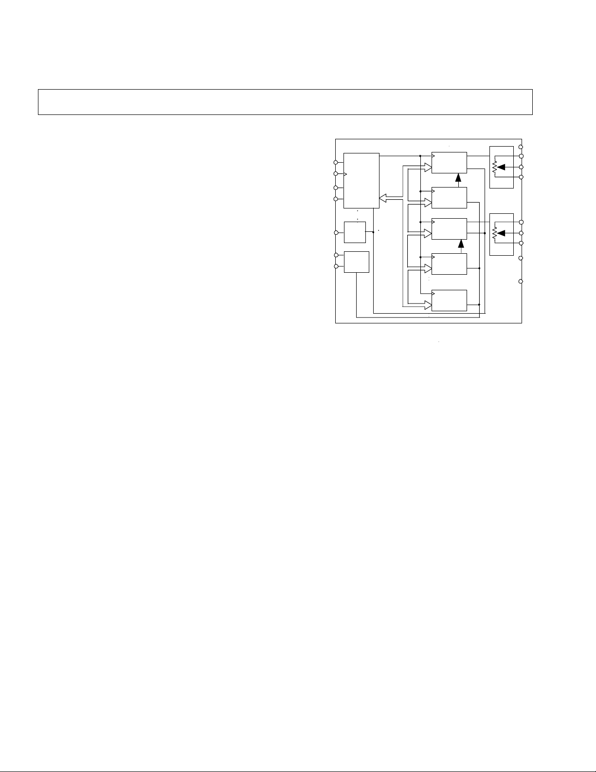
GENERAL DESCRIPTION
The AD5235 provides a dual channel, digitally controlled variable
resistor (VR) with resolutions of 1024 positions. These devices
perform the same electronic adjustment function as a potentiometer or
variable resistor. The AD5235’s versatile programming via a Micro
Controller allows multiple modes of operation and adjustment.
In the direct program mode a predetermined setting of the RDAC
register can be loaded di rect ly from the micro controller. Another key
mode of operation allows the RDAC register to be refreshed with the
setting previously stored in the EEMEM register. When changes are
made to the RDAC register to establish a new wiper position, the
value of the setting can be saved into the EEMEM by executing an
EEMEM save operation. Once the settings are saved in the EEMEM
register, these values will be transferred automatically to the RDAC
register to set the wiper position at system power ON. Such operation
is enabled by the internal preset strobe and the preset can also be
accessed externally.
An internal scratch pad RDAC register can be programmed by the
micro controller to set the resist ance between terminals W-and-B.
Once the target value is achi eved, the RDAC content register can be
placed in the non-volatile memory for automatic recall during Power
Up.
The AD5235 is available in the thin TSSOP-16 package. All parts are
guaranteed to operate over the extended industrial temperature range
of -40°C to +85°C.
FUNCTIONAL BLOCK DIAGRAMS
CS
CLK
SDI
SDO
WP
RDY
PR
ADDRESS
DECODE
SERIAL
INP UT
REGISTER
PWR ON
PRESET
EEMEM
CONTROL
GND
REGISTER
EEMEM1
REGISTER
EEMEM2
RDAC1
RDAC2
SPARE
EEMEM
AD5235
RDAC1
RDAC2
V
DD
A1
W1
B1
A2
W2
B2
V
SS
GND
REV PrD 6 Nov 2000
Information furnished by A nalog Devices i s believed to be ac curate and reliable. However , no
responsibility is assumed by Analog Devices for its use; nor for any infringements of patents or
other rights of third par ties whic h may res ult from i ts use. No l icense i s granted by i mplic ation
or otherwise under any patent or patent rights of Analog Devices.
One Technology Way, P.O. Box 9106,
Tel: 781/329-4700 Fax:781/326-8703
Norwood, MA 02062-9106 U.S.A.
Page 2

PRELIMINARY TECHNICAL DATA
Nonvolatile Memory Digital Potentiometers
ELECTRICAL CHARACTERISTICS 25K, 250K OHM VERSIONS
= +V
, VB = 0V, -40°C < TA < +85°C unless otherwise noted.)
DD
AD5235
(VDD = +3V±10% or +5V±10% and VSS=0V, VA
Parameter Symbol Conditions Min Typ1 Max Units
DC CHARACTERISTICS RHEOSTAT MODE Specifications apply to all VRs
Resistor Diff erential NL2 R-DNL RWB, VA=NC -1 ±1/4 +1 LSB
Resistor Nonlinear ity2 R-INL RWB, VA=NC -2 ±1/2 +2 LSB
Nominal resistor tolerance ∆R TA = 25°C, VAB = VDD,Wiper (VW) = No connect -30 30 %
Resistance Temperature Coefficent RAB/∆T V
Wiper Resistance RW I
Wiper Resistance RW I
DC CHARACTERISTICS POTENTIOMETER DIVIDER MODE Specifications apply to all VRs
Resolution N 10 Bits
Integral Nonlinearity3 INL –2 ±1/2 +2 LSB
Differential Nonlinearity3 DNL –1 ±1/4 +1 LSB
Voltage Divider Temperat ure Coefficent ∆VW/∆T Code = Half-scale 15 ppm/°C
Full-Scale Error V
Zero-Scale Error V
Code = Full-scale –3 -1 +0 LSB
WFSE
Code = Zero-s cale 0 +1 +3 LSB
WZSE
RESISTOR TERMINALS
Voltage Range4 V
Capacitance5 Ax, Bx C
VSS V
A,B,W
f = 1 MHz, measured to GND, Code = Hal f-scale 45 pF
A,B
Capacitance5 Wx CW f = 1 MHz, measured to GND, Code = Half-scale 60 pF
Common-mode Leakage Current7 I
V
CM
DIGITAL INPUTS & OUTPUTS
Input Logic High VIH with respect to GND 0.3•VDD V
Input Logic Low VIL with respect to GND 0.7•VDD V
Output Logic High VOH R
Output Logic High VOH IOH = 40µA, V
Output Logic Low VOL I
Input Current IIL V
Input Capacitance5 C
5 pF
IL
POWER SUPPLIES
Single-Supply Power Range VDD V
Dual-Supply Power Range VDD/VSS VSS = 0V ±2.2 ±2.7 V
Positive Supply Current IDD V
Programming Mode Current I
Read Mode Current I
VIH = VDD or VIL = GND 15 mA
DD(PG)
VIH = VDD or VIL = GND 650 µA
DD(READ)
Negative Supply Current ISS V
Power Dissipation6 P
V
DISS
Power Supply Sensitiv ity PSS ∆VDD = +5V ±10% 0.002 0.01 %/%
DYNAMIC CHARACTERISTICS
5, 7
Bandwidth –3dB BW_25K R = 12KΩ 400 KHz
Total Harmonic Distortion THDW V
VW Settling Time tS V
25K/250K 0.6/3/6 µs
Resistor Noise Voltage e
RWB = 10KΩ, f = 1KHz 9 nV√Hz
N_WB
Crosstalk CT V
VR making full scale change -65 dB
= VDD, Wiper (VW) = No Connect 50 ppm/°C
AB
= 1 V/R, VDD = +5V 50 100 Ω
W
= 1 V/R, VDD = +3V 200 Ω
W
V
DD
= VB = VDD/2 0.01 1 µA
A
= 2.2KΩ to +5V 4.9 V
PULL-UP
= +5V 4 V
= 1.6mA, V
OL
= 0V or VDD ±1 µA
IN
= 0V 2.7 5.5 V
SS
= VDD or VIL = GND 2 20 µA
IH
= VDD or VIL = GND, V
IH
= VDD or VIL = GND 0.05 mW
IH
=1Vrms, VB = 0V, f=1KHz 0.003 %
A
= VDD, VB=0V, 50% of final value
A
= VDD, VB = 0V, Measue VW with adjacent
A
LOGIC
= +5V 0.4 V
LOGIC
= 2.5V, V
DD
= -2.5V 10 µA
SS
REV PrD 6 NOV, 2000 2
Information contained i n this Product Concept data s heet describes a product in the early def i ni tion stage. There is no guarantee that the
information contained here will become a final product in its present form. For lat est information contact Walt Heinzer/Analog Devic es, Santa Clara,
CA. TEL(408)562-7254; FAX (408)727-1550; walt.heinzer@analog.com
Page 3
PRELIMINARY TECHNICAL DATA
Nonvolatile Memory Digital Potentiometers
AD5235
ELECTRICAL CHARACTERISTICS 25K, 250K OHM VERSIONS
= +V
, VB = 0V, -40°C < TA < +85°C unless otherwise noted.)
DD
Parameter Symbol Conditions Min Typ1 Max Units
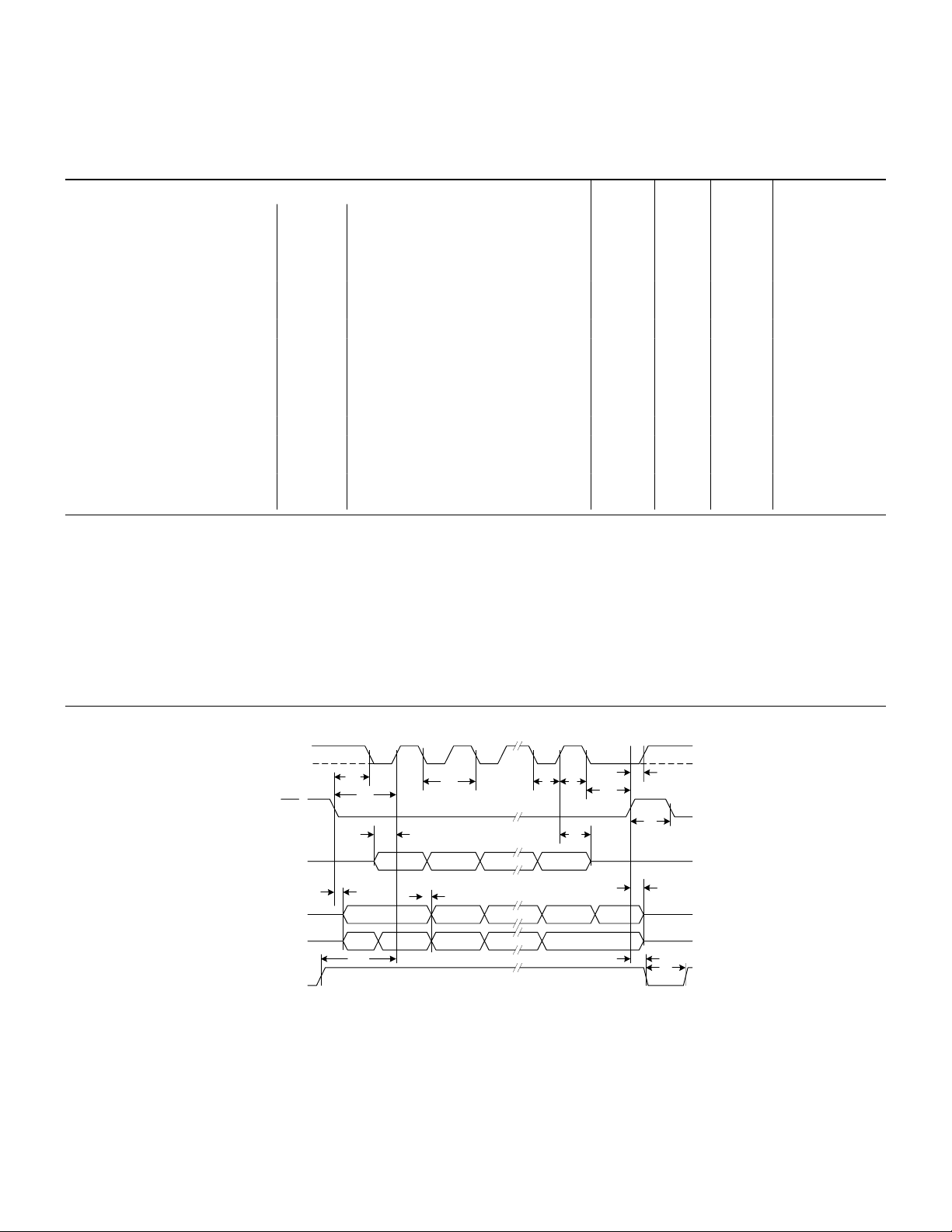
INTERFACE TIMING CHARACTERISTICS applies to all parts(Notes 5, 8)
Clock Cycle Time t 1 20 ns
Input Clock Pulse Width t 2 , t 3 Clock level high or low 10 ns
CS Setup Time t
10 ns
4
Data Setup Time t 5 From Positive CLK transition 5 ns
Data Hold Time t 6 From Positive CLK transition 5 ns
CLK Shutdown Time t 7 0 ns
CS Rise to Clock Rise Setup t
CS High Pulse Width t
CLK to SDO Propagation Delay9 t
Store to Nonvolatile EEMEM Save Time10 t
CS to SDO - SPI line acquire t
CS to SDO - SPI line release t
RDY Rise to CLK Rise t
Startup Time t
CLK Setup Time t
10 ns
8
10 ns
9
R
10
Applies to Command 2H, 3H 25 ms
11
ns
12
ns
13
ns
14
ms
15
For 1 CLK period (t4 - t3 = 1 CLK period) ns
16
L
Preset Pulse Width tPR 50 ns
NOTES:
1. Typicals represent average readings at +25°C and VDD = +5V.
2. Resistor position nonlinearity error R-INL is the deviation from an ideal value measured between the maximum resistance and the minimum resistance wiper positions. R-DNL measures the relative step
change from ideal between successive tap positions. Parts are guaranteed monotonic. See figure 20 test circuit. I
3. INL and DNL are measured at V
DNL specification limits of ±1LSB maximum are Guaranteed Monotonic operating conditions. See Figure 19 test circuit.
4. Resistor terminals A,B,W have no limitations on polarity with respect to each other.
5. Guaranteed by design and not subject to production test.
6. P
7. All dynamic characteristics use V
8. See timing diagram for location of measured values. All input control voltages are specified with t
9. Propagation delay depends on value of V
10. Low only for commands 8, 9,10, 2, 3: CMD_8 ~ 1ms; CMD_9,10 ~0.1ms; CMD_2,3 ~20ms.
is calculated from (IDD x VDD=+5V).
DISS
measured using both V
with the RDAC configured as a potentiometer divider similar to a voltage output D/A converter. VA = VDD and VB = 0V.
W
= +5V.
DD
= +3V or +5V.
DD
, R
DD
PULL_UP
, and CL see applications text.
= 1KΩ, CL < 20pF 1 25 ns
= VDD/R for both VDD=+3V or VDD=+5V.
W
=2.5ns(10% to 90% of 3V) and timed from a voltage level of 1.5V. Switching characteristics are
R=tF
(VDD = +3V±10% to +5V±10% and VSS=0V, VA
Timing Diagram
CLK
t
t
CS
SDI
SDO
SDO
16
t
4
t
5
t
1
MSB
t
12
1
2
t
14
MSB
MSB
t
10
3
LSB
LSB
t2t
t
6
LSB
RDY
SDO1 CLK IDLES LOW SDO2 CLK IDLES HIGH
Figure 1. Timing Diagram
REV PrD 6 NOV, 2000 3
Information contained i n this Product Concept data s heet describes a product in the early def i ni tion stage. There is no guarantee that the
information contained here will become a final product in its present form. For lat est information contact Walt Heinzer/Analog Devic es, Santa Clara,
CA. TEL(408)562-7254; FAX (408)727-1550; walt.heinzer@analog.com
8
t
7
t
9
t
13
t
15
t
11
Page 4

PRELIMINARY TECHNICAL DATA
Nonvolatile Memory Digital Potentiometers
Absolute Maximum Rating (
noted)
VDD to GND..............................................................-0.3, +7V
VSS to GND................................................................. 0V, -7V
to VSS.........................................................................+7V
V
DD
V
, VB, VW to GND.................................................VSS, VDD
A
– BX, AX – WX, BX – WX......................................±20mA
A
X
Ox to GND................................................................... 0V, VDD
Digital Inputs & Output Voltage to GND ..................0V, +7V
Operating Temperature Range......................... -40°C to +85°C
Maximum Junction Temperature (T
Storage Temperature ..................................... -65°C to +150°C
Lead Temperature (Soldering, 10 sec)..........................+300°C
Thermal Resistance
θ
JA,
TSSOP-16......................................................180°C/W
Package Power Dissipation = (TJMAX - TA) / θJA
Ordering Guide
#CHs/ Temp Package Package
Model k Ohm Range Description Option
AD5235BRU25 X2/25 -40/+85°C TSSOP-16 RU-16
AD5235BRU250 X2/250 -40/+85°C TSSOP-16 RU-16
The AD5235 contains 16,000 transistors.
Die size: 100 x 105 mil = 10,500 sq. mil
TA = +25°C, unless otherwise
)...................+150°C
MAX
J
AD5235
PIN CONFIGURATION
CLK
1
2
SDI
3
SDO
4
GND
5
V
SS
6
A1
7
W1
8
B1
AD5235
RDY
16
15
CS
CS
CS CS
14
PR
PR
PRPR
13
WP
WP
WPWP
12
V
DD
11
A2
10
W2
9
B2
AD5235 PIN FUNCTION DESCRIPTION
# Name Description
1 CLK Serial Input Register clock pin. Shifts in one bit at
a time on positive clock edges.
2 SDI Serial Data Input Pin. Shifts in one bit at a time
on positive clock CLK edges.
3 SDO Serial Data Output Pin. Open Drain Output
requires external pull-up resistor. Commands 9
and 10 activate the SDO output. See Instruction
operation Truth Table. Table 2.
4 GND Ground pin, logic ground reference
5 V
6 A1 A t erminal of RDAC1.
7 W1 Wiper terminal of RDAC1,
8 B1 B terminal of RDAC1.
9 B2 B terminal of RDAC2.
10 W2 Wiper terminal of RDAC2,
11 A2 A terminal of RDAC2.
12 VDD Positive Power Supply Pin. Should be ≥ the
13 WP Write Protect Pin. Prevents any changes to the
14 PR Hardware over ride preset pin. Refreshes the
15 CS S eri al Register chip select active low. Serial
16 RDY Ready. Active-high open drain output. Identifies
Negative Supply. Connect to zero volts for single
SS
supply applications.
ADDR(RDAC1) = 0H.
ADDR(RDAC3) = 1
.
H
input-logic HIGH voltage.
present EEMEM co ntents when active low.
scratch pad register with current contents of the
EEMEM register. Factory default loads midscale
512
.
10
register operation takes p lace when CS returns to
logic high.
completion of commands 2, 3, 8, 9, 10.
REV PrD 6 NOV, 2000 4
Information contained i n this Product Concept data s heet describes a product in the early def i ni tion stage. There is no guarantee that the
information contained here will become a final product in its present form. For lat est information contact Walt Heinzer/Analog Devic es, Santa Clara,
CA. TEL(408)562-7254; FAX (408)727-1550; walt.heinzer@analog.com
Page 5

PRELIMINARY TECHNICAL DATA
Nonvolatile Memory Digital Potentiometers
OPERATIONAL OVERVIEW
• Permanent storage of the present scratch pad RDAC register
values into the corresponding EEMEM register
The AD5235 digital potentiometer is designed to operate as a true
variable resistor replacement devi ce for analog signals that remain
within the terminal voltage range of V
voltage range is limited to a V
- VSS<5.5V. Control of the digital
DD
SS<VTERM<VDD
. The basic
potentiometer allows both scratch pad register (RDAC register)
changes to be made, as well as 100,000 times of nonvolatile
electrically erasable memory (EEMEM) register operations. The
EEMEM update process takes approximately 20.2ms, during this
time the shift register is locked preventing any changes from taking
place. The RDY pin flags the co mpletion of this EEMEM save.
The EEMEM retention is designed to last 10 years without refresh.
The scratch pad register can be changed incrementally by using the
software controlled Increment/Decrement instruction or the Shift
Left/Right instruction co mmand. On ce an Increment, Decrement or
Shift command has been loaded into the shift register, subsequent
CS strobes will repeat this command. This is useful for push button
control applications. Alternately the scratch pad register can be
• 30 bytes of user addressable electrical-erasable memory
The serial interface of AD5235 digital potentiometer uses a 24-bit
serial word loaded with MSB first. The format of the SPI
compatible word is shown in Table 1. The Command Bits (Cx)
control the op erat i on of the digital po tentiometer according to the
command instruction shown in Table 2. The Address Bits (Ax)
determine which register is activated. The Data Bits (Dx) are the
values that are loaded into the decoded register. The last
instruction executed prior to a period of no programming activity
should be the NOP instruction. This will place the in t ernal logic
circuitry in a minimum power dissipation state.
PR
VALID
COMMAND
COUNTER
COMMAND
PROCESSOR
& ADDRESS
DECODE
programmed with any position value using the standard SPI serial
interface mode by loading the representative data word. The
scratch pad register can be loaded with the current contents of the
CLK
SERIAL
REGISTER
nonvolatile EEMEM register under the program control. At system
power ON, the default value of the scratch pad memory is the value
previously saved in th e EEMEM register. The factory EEMEM
preset value is midscale 512
.
10
A serial data output pin is available for daisy chaining and for
readout of the internal register contents. The serial input data
register uses a 24-bit instruction/address/data WORD. The writeprotect (WP) pin provides a hardware EEMEM protection feature
disabling any changes of the present EEMEM contents.
SERIAL DATA INTERFACE
The AD5235 contains a four-wire SPI compatible digital interface
(SDI, SDO, CS, and CLK). Key features of this interface in cl ude:
CS
SDI
Figure 2. Equivalent Digital Input-Output Logic
The equivalent serial data input and output logic is shown in figure
2. The open drain output SDO is disabled whenever chip select CS
is logic high. The SPI interface can be used in two slave modes
CPHA=1, CPOL=1 and CPHA=0, CPOL=0. CPHA and CPOL
refer to the control bits, which dictate SPI timing in the following
microprocessors/MicroConverters: ADuC812/824, M68HC11, and
MC68HC16R1/916R1.
• Independently Programmable Read & Write to all registers
• Direct parallel refresh of all RDAC wiper registers from
corresponding EEMEM registers
Table 1. AD5235 24-bit Serial Data Word
M
L
S
B
AD5235
C3 C2 C1 C0 A3 A2 A1 A0 X X X X X X D9 D8 D7 D6 D5 D4 D3 D2 D1 D0
Command bits are identified as Cx, address bits are Ax, and data bits are Dx. Command instruction codes are defined in table 2.
AD5235
+5V
R
PULLUP
SDO
GND
S
B
REV PrD 6 NOV, 2000 5
Information contained i n this Product Concept data s heet describes a product in the early def i ni tion stage. There is no guarantee that the
information contained here will become a final product in its present form. For lat est information contact Walt Heinzer/Analog Devic es, Santa Clara,
CA. TEL(408)562-7254; FAX (408)727-1550; walt.heinzer@analog.com
Page 6

PRELIMINARY TECHNICAL DATA
Nonvolatile Memory Digital Potentiometers
AD5235
Table 2. AD5235 Instruction/Operation Truth Table
Inst
Instruction Byte 1
B15 •••••••••••••••• B8
No.
C3 C2 C1 C0 A3 A2 A1 A0 X ••• D9 D8 D7 ••• D0
0 0 0 0 0 X X X X X ••• X X X ••• X
1 0 0 0 1 << ADDR >> X ••• X X X ••• X
2 0 0 1 0 << ADDR >> X ••• X X X ••• X
3 0 0 1 1 << ADDR >> X ••• D9 D8 D7 ••• D0
4 0 1 0 0 << ADDR >> X ••• X X X ••• X
5 0 1 0 1 X X X X X ••• X X X ••• X
6 0 1 1 0 << ADDR >> X ••• X X X ••• X
7 0 1 1 1 X X X X X ••• X X X ••• X
8 1 0 0 0 0 0 0 0 X ••• X X X ••• X
9 1 0 0 1 << ADDR >> X ••• X X X ••• X
10 1 0 1 0 << ADDR >> X ••• X X X ••• X
11 1 0 1 1 << ADDR >> X ••• D9 D8 D7 ••• D0
12 1 1 0 0 << ADDR >> X ••• X X X ••• X
13 1 1 0 1 X X X X X ••• X X X ••• X
14 1 1 1 0 << ADDR >> X ••• X X X ••• X
15 1 1 1 1 X X X X X ••• X X X ••• X
Data Byte 1
B15 •••• B8
Data Byte 0
B7 ••• B0
Operation
NOP: Do nothing
Write contents of EEMEM(ADDR) to RDAC(ADDR)
Register
SAVE WIPER SETTING: Write contents of
RDAC(ADDR) to EEMEM(ADDR)
Write contents of Serial Register Data Byte 0 & 1 to
EEMEM(ADDR)
DEC 6dB: Right Shift contents of RDAC(ADDR) ,
LSB rolls over to MSB position
DEC All 6dB: Right Shift contents of all RDAC
Registers, LSB rolls over to MSB position
Decrement contents of RDAC(ADDR) by One, does
not rollover at zero-scale
Decrement contents of all RDAC Registers by One,
does not rollover at zero-scale
RESET: Load all RDACs with their corresponding
EEMEM previously-saved values
Write contents of EEMEM(ADDR) to Serial Register
Data Byte 0 & 1
Write contents of RDAC(ADDR) to Serial Register
Data Byte 0 & 1
Write contents of Serial Register Data Byte 0 &1 to
RDAC(ADDR)
INC 6dB: Left Shift contents of RDAC(ADDR), stops
at all 'Ones'.
INC All 6dB: Right Shift contents of all RDAC
Registers, stops at all 'Ones'.
Increment contents of RDAC(ADDR) by One, does
not rollover at full-scale stops at all 'Ones'.
Increment contents of all RDAC Registers by One,
does not rollover at full-scale stops at all 'Ones'.
NOTES:
1. The SDO output shifts-out the last 24-bits of data clocked into the serial register for daisy chain operation. Exception,
following Instruction #9 or #10 the selected internal register data will be present in data byte 0 & 1. Instructions following
#9 & #10 must be a full 24-bit data word to completely clock out the contents of the serial register.
2. The RDAC register is a volatile scratch pad register that is refreshed at power ON from the corresponding non-volatile
EEMEM register.
3. The increment, decrement and shift commands ignore the contents of the shift register Data Byte 0.
4. Execution of the Operation column noted in the table takes place when the CS strobe returns to logic high.
.
REV PrD 6 NOV, 2000 6
Information contained i n this Product Concept data s heet describes a product in the early def i ni tion stage. There is no guarantee that the
information contained here will become a final product in its present form. For lat est information contact Walt Heinzer/Analog Devic es, Santa Clara,
CA. TEL(408)562-7254; FAX (408)727-1550; walt.heinzer@analog.com
Page 7

PRELIMINARY TECHNICAL DATA
Nonvolatile Memory Digital Potentiometers
Detail Potentiometer Operation
The actual structure of th e RDAC is designed to emulate the
performance of a mechanical potentiometer. The RDAC contains a
string of connected resistor segments, with an array of analog
switches that act as the wiper connection to several points along the
resistor array. The number of points is the resolution of the device.
The AD5235 has 1024 connection points allowing it to provide
better than 0.5% set-ability resolution. Figure 3 provides an
equivalent diagram of the connections between the three terminals
that make up one channel of the RDAC. The SW
always be ON while one of the switches SW(0) to SW(2
be ON one at a time depends upon the resistance step decoded from
the Data Bits. Note that there are two 50Ω wiper resistances, R
The resistance contributed by R
calculating the output resistance. R
SW
+ SWX and SWB + SWX for A-to-Wiper and B-to-Wiper
A
must be accounted for when
W
is the sum of the resistances of
W
respectively.
SW
RDAC
WIPER
REGISTER
&
DECODER
RS = RAB /2
R
R
R
N
SW(2N-1)
S
SW(2N-2)
S
SW(1 )
S
SW(0 )
A
and SWB will
A
N
-1) will
A
X
W
X
.
W
ladder until the last tap point is reached at R
AD5235
=25025Ω. See figure
WB
3 for a simplified diagram of the equivalent RDAC circuit.
The general equation, which determines the digitally programmed
output resistance between Wx and Bx, is:
(Dx) = (Dx/2N) * RAB + R
R
WB
W
eqn. 1
Where N is the resolution of the VR, Dx is the data contained in
the RDACx latch, and R
Since N=10 and R
R
(Dx) = (Dx/1024) * RAB + 50Ω
WB
W
is the nominal end-to-end resistance.
AB
=50Ω for AD5235, eqn. 1 becomes:
eqn. 2
For example, when VB = 0V and A–terminal is open circuit the
following output resistance values will be set for the following
RDAC latch codes (applies to RAB=25KΩ potentiometers):
Dx R
Output State
WB
(DEC) (Ω)
1023 25025Ω Full-Scale
512 12500Ω Mid-Scale
1 74Ω 1 LSB
0 50Ω Zero-S cal e (Wiper contact resistance)
Note that in the zero- scale condition a finit e wiper resi stance of
50Ω is present. Care should be taken to limit the current flow
between W and B in this state to no more than 20mA to avoid
degradation or possible destruction of the internal switch contact.
DIGITAL
CIRCUITRY
OMITTED FOR
CLARITY
SW
B
B
X
Figure 3. Equivalent RDAC structure
PROGRAMMING THE VARIABLE RESISTOR
Rheostat Operation
The nominal resistance of the RDAC between terminals A and B
are available with values of 25KΩ, and 250KΩ. The final digits of
the part number determine the nominal resistance value, e.g., 25KΩ
= 25; 250KΩ = 250. The nominal resistance (R
) of the AD5235
AB
Figure 4. Symmetrical RDAC Operation
VR has 1024 contact points accessed by the wiper terminal, plus
the B terminal contact. The 10-bit data word in the RDAC latch is
decoded to select one of the 1024 possible settings. The wiper's
first connection starts at the B terminal for data 00
terminal connection h as a wiper contact resistance, R
regardless of what the nominal resistan ce R
. This B–
H
of 50Ω,
W
is. The second
AB
connection (25KΩ part) is the first tap point where RWB =74Ω [RWB
=RAB/1024 + RW = 24Ω+50Ω)] for data 01H. The third connection
is the next tap point representing R
=49+50=99Ω for data 02H.
WB
Each LSB data value increase moves the wiper u p the resistor
REV PrD 6 NOV, 2000 7
Information contained i n this Product Concept data s heet describes a product in the early def i ni tion stage. There is no guarantee that the
information contained here will become a final product in its present form. For lat est information contact Walt Heinzer/Analog Devic es, Santa Clara,
CA. TEL(408)562-7254; FAX (408)727-1550; walt.heinzer@analog.com
Like the mechanical potenti ometer the RDAC replaces, the
AD5235 part is totally symmetrical. The resistance between the
wiper W and terminal A also produces a digitally controlled
resistance R
. Figure 4 shows the symmetrical programmability
WA
of the various terminal conn ections. When these terminals are u sed,
the B–terminal should be tied to the wiper. Setting the resistance
value for RWA starts at a maximum value of resistance and
decreases as the data loaded in the latch is increased in value. The
general equation for this operation is:
Page 8

PRELIMINARY TECHNICAL DATA
Nonvolatile Memory Digital Potentiometers
RWA(Dx) = [ (2N-Dx)/2N ] * RAB + R
W
Similarly, eqn. 3 becomes:
R
(Dx) = [ (1024-Dx)/1024 ] * RAB + 50Ω eqn. 4
WA
For example, when VA = 0V and B–terminal is tied to the wiper W
the following output resistance values will be set for the following
RDAC latch codes (applies to RAB=10KΩ potentiometers):
Dx R
Ou tput State
WA
(DEC) (Ω)
1023 74 Full-Scale
512 12500 Mid-Scale
1 25000 1 LSB
0 25050 Zero-Scale
A ±1% typical distribution of RAB from channel-to-channel occurs
within the same package. On the other hand, d evice to device
matching is process lot dependent such that a maximum of ±30%
variation is possible. The change in RAB with temperature has a 50
ppm/°C temperature coefficient.
PROGRAMMING THE POTENTIOMETER DIVIDER
Voltage Output Operation
eqn. 3
ESD PROTECTION CIRCUITS
INPUT S
LOGIC
PINS
GND
Figure 5A. Equivalent Digital Input ESD Protection
V
DD
OUTPUTS
GND
Figure 5B. Equivalent Digital Output ESD Protection
AD5235
V
DD
O1 & O2
PINS
The digital potentiometer easily generates an output voltage
proportional to the input voltage applied to a given terminal. For
example connecting A–terminal to +5V and B–terminal to ground
produces an output voltage at the wiper which can be any value
starting at zero volts and up to 1 LSB less than +5V. Each LSB of
voltage is equal to the voltage applied across terminal AB divided
N
by the 2
resolution of the potentiometer divider. The general
equation defining the output voltage with respect to ground for any
given input voltage applied to terminals AB is:
(Dx) = Dx/2N * VAB + VB eqn. 5
V
W
Since N=10,
(Dx) = (Dx/1024) * VAB + V
V
W
eqn. 6
B
Operation of the digital potentiometer in the divider mode results in
more accurate operation over temperature. Here the output voltage
is dependent on the ratio of the internal resistors and not the
absolute value. Therefore, the drift reduces to 15ppm/°C.
V
DD
OUTPUTS
SDO
PIN
GND
Figure 5C. Equivalent SDO Output ESD Protection Circuit
Figure 5 shows the equivalent ESD protection circuit for digital
pins. Figure 6 shows the equivalent analog-terminal protection
circuit for the variable resistors.
POTENTIOMETER
TERM INALS
A, B, W
PINS
V
SS
Figure 6. Equivalent VR-Terminal ESD Protection
REV PrD 6 NOV, 2000 8
Information contained i n this Product Concept data s heet describes a product in the early def i ni tion stage. There is no guarantee that the
information contained here will become a final product in its present form. For lat est information contact Walt Heinzer/Analog Devic es, Santa Clara,
CA. TEL(408)562-7254; FAX (408)727-1550; walt.heinzer@analog.com
Page 9

PRELIMINARY TECHNICAL DATA
Nonvolatile Memory Digital Potentiometers
TEST CIRCUITS
Figures 7 to 15 define the test conditions used in the product
specification's table.
Figure 7. Potentiometer Divider Nonlinearity error test circuit
(INL, DNL)
Figure 8. Resistor Position Nonlinearity Error (Rheostat Operation;
R-INL, R-DNL)
Figure 12. Non-Inverting Gain test circuit
Figure 13. Gain Vs Frequency test circuit
AD5235
Figure 9. Wiper Resistance test Circuit
Figure 10. Power supply sensitivity test circuit (PSS, PSSR)
Figure 11. Inverting Gain test Circuit
Figure 14. Incremental ON Resistan ce Test Circuit
Figure 15. Common Mode Leakage current test circuit
TYPICAL PERFORMANCE GRAPHS
TBD
REV PrD 6 NOV, 2000 9
Information contained i n this Product Concept data s heet describes a product in the early def i ni tion stage. There is no guarantee that the
information contained here will become a final product in its present form. For lat est information contact Walt Heinzer/Analog Devic es, Santa Clara,
CA. TEL(408)562-7254; FAX (408)727-1550; walt.heinzer@analog.com
Page 10

PRELIMINARY TECHNICAL DATA
Nonvolatile Memory Digital Potentiometers
OUTLINE DIMENSIONS
Dimensions shown in inches and (mm)
AD5235
REV PrD 6 NOV, 2000 10
Information contained i n this Product Concept data s heet describes a product in the early def i ni tion stage. There is no guarantee that the
information contained here will become a final product in its present form. For lat est information contact Walt Heinzer/Analog Devic es, Santa Clara,
CA. TEL(408)562-7254; FAX (408)727-1550; walt.heinzer@analog.com
 Loading...