

Datasheet AD5232BRU50-REEL7, AD5232BRU50, AD5232BRU100-REEL7, AD5232BRU100, AD5232BRU10-REEL7 Datasheet (Analog Devices)
...Page 1
REV. 0
Information furnished by Analog Devices is believed to be accurate and
reliable. However, no responsibility is assumed by Analog Devices for its
use, nor for any infringements of patents or other rights of third parties that
may result from its use. No license is granted by implication or otherwise
under any patent or patent rights of Analog Devices.
a
AD5232
One Technology Way, P.O. Box 9106, Norwood, MA 02062-9106, U.S.A.
Tel: 781/329-4700 www.analog.com
Fax: 781/326-8703 © Analog Devices, Inc., 2001
*
8-Bit Dual Nonvolatile Memory
Digital Potentiometer
FEATURES
Nonvolatile Memory Preset Maintains Wiper Settings
Dual Channel, 256-Position Resolution
Full Monotonic Operation DNL < 1 LSB
10 k, 50 k, 100 k Terminal Resistance
Linear or Log Taper Settings
Push-Button Increment/Decrement Compatible
SPI-Compatible Serial Data Input with Readback
Function
3 V to 5 V Single Supply or 2.5 V Dual Supply
Operation
14 Bytes of User EEMEM Nonvolatile Memory for
Constant Storage
Permanent Memory Write Protection
100-Year Typical Data Retention T
A
= 55C
APPLICATIONS
Mechanical Potentiometer Replacement
Instrumentation: Gain, Offset Adjustment
Programmable Voltage-to-Current Conversion
Programmable Filters, Delays, Time Constants
Line Impedance Matching
Power Supply Adjustment
DIP Switch Setting
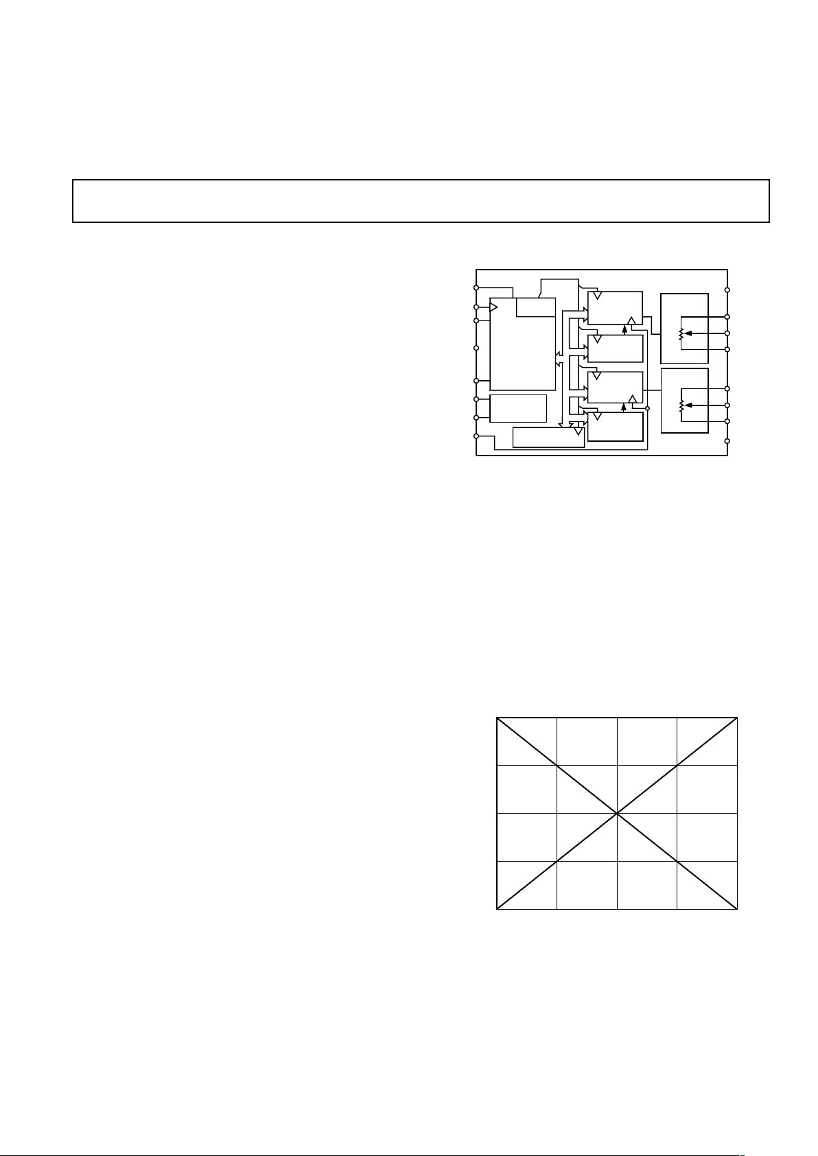
GENERAL DESCRIPTION
The AD5232 device provides a nonvolatile, dual-channel,
digitally controlled variable resistor (VR) with 256-position
resolution. These devices perform the same electronic adjustment function as a potentiometer or variable resistor. The
AD5232’s versatile programming via a microcontroller allows
multiple modes of operation and adjustment.
In the direct program mode a predetermined setting of the RDAC
register can be loaded directly from the microcontroller.
Another key mode of operation allows the RDAC register to be
refreshed with the setting previously stored in the EEMEM
register. When changes are made to the RDAC register to establish a new wiper position, the value of the setting can be saved
into the EEMEM by executing an EEMEM save operation.
Once the settings are saved in the EEMEM register these values
will be automatically transferred to the RDAC register to set the
wiper position at system power ON. Such operation is enabled
by the internal preset strobe and the preset can also be accessed
externally.
All internal register contents can be read out of the serial data
output (SDO). This includes the RDAC1 and RDAC2 registers,
the corresponding nonvolatile EEMEM1 and EEMEM2 registers, and the 14 spare USER EEMEM registers available for
constant storage.
*Patent pending.
FUNCTIONAL BLOCK DIAGRAM
RDAC1
REGISTER
EEMEM1
RDAC2
REGISTER
EEMEM
CONTROL
14 BYTES
USER EEMEM
EEMEM2
AD5232
RDAC1
RDAC2
CS
CLK
WP
PR
SDI
GND
SDO
RDY
SDO
SERIAL
INTERFACE
ADDR
DECODE
V
DD
V
SS
A1
W1
B1
A2
W2
B2
SDI
The basic mode of adjustment is the increment and decrement
command controlling the present setting of the Wiper position
setting (RDAC) register. An internal scratch pad RDAC register
can be moved UP or DOWN one step of the nominal terminal
resistance between terminals A and B. This linearly changes the
wiper to B terminal resistance (R
WB
) by one position segment of
the devices’ end-to-end resistance (R
AB
). For exponential/logarithmic changes in wiper setting, a left/right shift command
adjusts levels in ±6 dB steps, which can be useful for audio and
light alarm applications.
The AD5232 is available in a thin TSSOP-16 package. All parts
are guaranteed to operate over the extended industrial temperature range of –40°C to +85°C. An evaluation board is available,
Part Number: AD5232EVAL.
CODE – Decimal
100
75
0
0 25664
PERCENT OF NOMINAL
END-TO-END RESISTANCE – % R
AB
128 192
50
25
R
WB
R
WA
Figure 1. Symmetrical RDAC Operation
Page 2

REV. 0
–2–
AD5232–SPECIFICA TIONS
ELECTRICAL CHARACTERISTICS, 10 k, 50 k, 100 k VERSIONS
( VDD = 3 V 10% or 5 V 10% and V
SS
= 0 V, VA = +VDD, VB = 0 V, –40C < TA < +85C unless otherwise noted.)
Parameter Symbol Conditions Min Typ1Max Unit
DC CHARACTERISTICS
RHEOSTAT MODE – Specifications Apply to All VRs
Resistor Differential Nonlinearity
2
R-DNL RWB, VA = NC –1 ±1/2 +1 LSB
Resistor Nonlinearity
2
R-INL RWB, VA = NC –0.4 +0.4 % FS
Nominal Resistor Tolerance ⌬R
AB
–40 +20 %
Resistance Temperature Coefficient ⌬R
AB
/⌬T 600 ppm/°C
Wiper Resistance R
W
IW = 100 µA, V
DD
= 5.5 V, Code = 1E
H
5 100 Ω
R
W
IW = 100 µA, V
DD
= 3 V, Code = 1E
H
200 Ω
POTENTIOMETER DIVIDER MODE — Specifications Apply to All VRs
Resolution N 8 Bits
Differential Nonlinearity
3
DNL –1 ±1/2 +1 LSB
Integral Nonlinearity
3
INL –0.4 +0.4 % FS
Voltage Divider Temperature Coefficient ⌬V
W
/⌬T Code = Half-Scale 15 ppm/°C
Full-Scale Error V
WFSE
Code = Full-Scale –3 0 % FS
Zero-Scale Error V
WZSE
Code = Zero-Scale 0 +3 % FS
RESISTOR TERMINALS
Terminal Voltage Range
4
V
A,B,W
V
SS
V
DD
V
Capacitance
5
Ax, Bx C
A,B
f = 1 MHz, Measured to GND,
Code = Half-Scale 45 pF
Capacitance
5
Wx C
W
f = 1 MHz, Measured to GND,
Code = Half-Scale 60 pF
Common-Mode Leakage Current
5, 6
I
CM
VW = VDD/2 0.01 1 µA
DIGITAL INPUTS AND OUTPUTS
Input Logic High V
IH
With Respect to GND, VDD = 5 V 2.4 V
Input Logic Low V
IL
With Respect to GND, VDD = 5 V 0.8 V
Input Logic High V
IH
With Respect to GND, VDD= 3 V 2.1 V
Input Logic Low V
IL
With Respect to GND, VDD = 3 V 0.6 V
Input Logic High V
IH
With Respect to GND, VDD = +2.5 V, 2.0 V
V
SS
= –2.5 V
Input Logic Low V
IL
With Respect to GND, VDD = +2.5 V, 0.5 V
V
SS
= –2.5 V
Output Logic High (SDO and RDY) V
OH
R
PULL-UP
= 2.2 kΩ to 5 V 4.9 V
Output Logic Low V
OL
IOL = 1.6 mA, V
LOGIC
= 5 V 0.4 V
Input Current I
IL
VIN = 0 V or V
DD
±2.5 µA
Input Capacitance
5
C
IL
4pF
POWER SUPPLIES
Single-Supply Power Range V
DD
VSS = 0 V 2.7 5.5 V
Dual-Supply Power Range V
DD/VSS
±2.25 ±2.75 V
Positive Supply Current I
DD
VIH = VDD or VIL = GND 3.5 10 µA
Programming Mode Current I
DD(PG)
VIH = VDD or VIL = GND 35 mA
Read Mode Current
7
I
DD(XFR)
VIH = VDD or VIL = GND 0.9 3 9 mA
Negative Supply Current I
SS
VIH = VDD or VIL = GND,
V
DD
= +2.5 V, V
SS
= –2.5 V 3.5 10 µA
Power Dissipation
8
P
DISS
VIH = VDD or VIL = GND 0.018 0.05 mW
Power Supply Sensitivity
5
PSS ⌬VDD = 5 V ±10% 0.002 0.01 %/%
Page 3

–3–
REV. 0
nV/√Hz
Parameter Symbol Conditions Min Typ1Max Unit
DYNAMIC CHARACTERISTICS
5, 9
Bandwidth –3 dB, BW_10 kΩ, R = 10 kΩ 500 kHz
Total Harmonic Distortion THD
W
VA = 1 V rms, VB = 0 V, f = 1 kHz,
R
AB
= 10 kΩ 0.022 %
THD
W
VA =1 V rms, VB = 0 V, f = 1 kHz,
R
AB
= 50 kΩ, 100 kΩ 0.045 %
V
W
Settling Time t
S
VDD=5V,VSS=0V,VA = VDD, VB = 0 V,
V
W
= 0.50% Error Band, Code 00H to 80
H
For RAB = 10 kΩ/50 kΩ/100 kΩ 0.65/3/6 µs
Resistor Noise Voltage e
N_WB
RWB = 5 kΩ, f = 1 kHz 9
Crosstalk (C
W1/CW2
)C
T
VA = VDD, VB = 0 V, Measure VW with
Adjacent VR Making Full-Scale Code Change
–5 nV-s
Analog Crosstalk (C
W1/CW2
)CTAV
A1
= VDD, V
B1
= 0 V, Measure V
W1
with VW2 = 5 V p-p @ f = 10 kHz,
Code1 = 80H; Code2 = FF
H
–70 dB
INTERFACE TIMING CHARACTERISTICS – Applies to All Parts
5, 10
Clock Cycle Time (t
CYC
)t
1
20 ns
CS Setup Time t
2
10 ns
CLK Shutdown Time to CS Rise t
3
1t
CYC
Input Clock Pulsewidth t 4 , t
5
Clock Level High or Low 10 ns
Data Setup Time t
6
From Positive CLK Transition 5 ns
Data Hold Time t
7
From Positive CLK Transition 5 ns
CS to SDO-SPI Line Acquire t
8
40 ns
CS to SDO-SPI Line Release t
9
50 ns
CLK to SDO Propagation Delay
11
t
10
RP = 2.2 kΩ, CL < 20 pF 50 ns
CLK to SDO Data Hold Time t
11
RP = 2.2 kΩ, CL < 20 pF 0 ns
CS High Pulsewidth
12
t
12
10 ns
CS High to CS High
12
t
13
4t
CYC
RDY Rise to CS Fall t
14
0ns
CS Rise to RDY Fall Time t
15
0.1 0.15 ms
Read/Store to Nonvolatile EEMEM
13
t
16
Applies to Command 2H, 3H, 9
H
25 ms
CS Rise to Clock Rise/Fall Setup t
17
10 ns
Preset Pulsewidth (Asynchronous) t
PRW
Not Shown in Timing Diagram 50 ns
Preset Response Time to RDY High t
PRESP
PR Pulsed Low to Refreshed
Wiper Positions 70 µs
FLASH/EE MEMORY RELIABILITY CHARACTERISTICS
Endurance
14
100 K Cycles
Data Retention
15
100 Years
NOTES
1
Typical parameters represent average readings at 25°C and VDD = 5 V.
2
Resistor position nonlinearity error R-INL is the deviation from an ideal value measured between the maximum resistance and the minimum resistance wiper
postions. R-DNL measures the relative step change from ideal between successive tap positions. Parts are guaranteed monotonic. IW ~ 50 µA @ V
DD
= 2.7 V and
IW ~ 400 µA @ V
DD
= 5 V for the R
AB
= 10 kΩ version, IW ~ 50 µA for the R
AB
= 50 kΩ and IW ~ 25 µA for the R
AB
= 100 kΩ version. See Figure 13.
3
INL and DNL are measured at VW with the RDAC configured as a potentiometer divider similar to a voltage output D/A converter. VA = VDD and VB = VSS. DNL
specification limits of ±1 LSB maximum are Guaranteed Monotonic operating conditions. See Figure 14.
4
Resistor terminals A, B, W have no limitations on polarity with respect to each other. Dual Supply Operation enables ground-referenced bipolar signal adjustment.
5
Guaranteed by design and not subject to production test.
6
Common-mode leakage current is a measure of the dc leakage from any terminal A, B, W to a common-mode bias level of VDD/2.
7
Transfer (XFR) Mode current is not continuous. Current consumed while EEMEM locations are read and transferred to the RDAC register. See TPC 9.
8
P
DISS
is calculated from (IDD VDD) + (ISS VSS).
9
All dynamic characteristics use VDD = +2.5 V and VSS= –2.5 V unless otherwise noted.
10
See timing diagram for location of measured values. All input control voltages are specified with tR = tF = 2.5 ns (10% to 90% of 3 V) and timed from a voltage level
of 1.5 V. Switching characteristics are measured using both VDD = 3 V or 5 V.
11
Propagation delay depends on value of VDD, R
PULL_UP
, and CL. See applications text.
12
Valid for commands that do not activate the RDY pin.
13
RDY pin low only for instruction commands 8, 9, 10, 2, 3, and the PR hardware pulse: CMD_8 ~ 1 ms; CMD_9,10 ~ 0.12 ms; CMD_2,3 ~ 20 ms. Device operation
at TA = –40°C and V
DD
< 3 V extends the save time to 35 ms.
14
Endurance is qualified to 100,000 cycles as per JEDEC Std. 22 method A117 and measured at VDD = 2.7 V, TA = –40°C to +85°C, typical endurance at 25°C is
700,000 cycles.
15
Retention lifetime equivalent at junction temperature (TJ) = 55°C as per JEDEC Std. 22, Method A117. Retention lifetime based on an activation energy of 0.6eV
will derate with junction temperature as shown in Figure 23 in the Flash/EE Memory description section of this data sheet. The AD5232 contains 9,646
transistors. Die size: 69 mil 115 mil, 7,993 sq. mil.
Specifications subject to change without notice
AD5232
Page 4
REV. 0
–4–
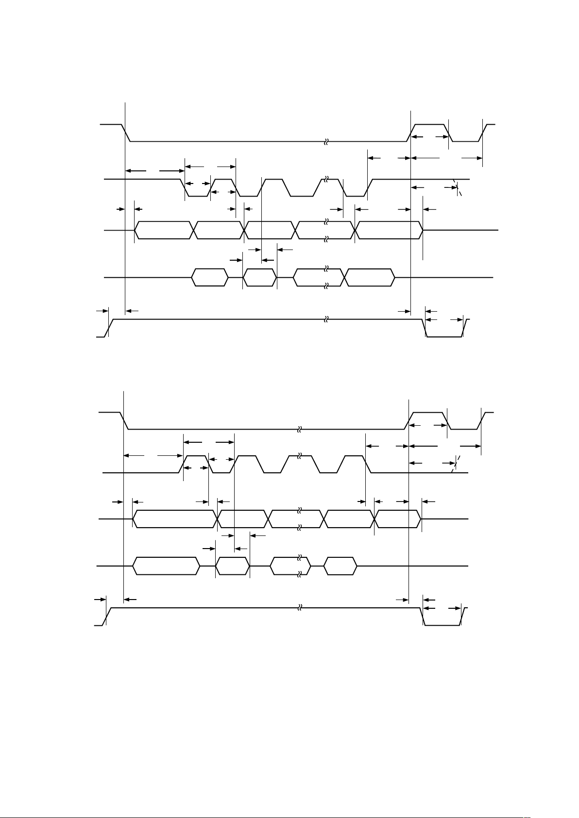
AD5232
CPOL = 1
t
12
t
13
t
3
t
17
t
9
t
11
t
5
t
4
t
2
t
1
CLK
t
8
*
MSB LSB OUT
MSB
LSB
RDY
CPHA = 1
t
10
t
7
t
6
t
14
t
15
t
16
*
NOT DEFINED, BUT NORMALLY LSB OF CHARACTER PREVIOUSLY TRANSMITTED.
THE CPOL = 1 MICROCONTROLLER COMMAND ALIGNS THE INCOMING DATA TO THE POSITIVE EDGE OF THE CLOCK.
CS
SDO
SDI
Figure 2a. CPHA = 1 Timing Diagram
t
12
t
13
t
3
t
17
t
9
t
11
t
5
t
4
t
2
t
1
CLK
CPOL = 0
t
8
MSB OUT LSB
SDO
MSB IN
LSB
SDI
RDY
CPHA = 0
t
10
t
7
t
6
t
14
t
15
t
16
*
NOT DEFINED, BUT NORMALLY MSB OF CHARACTER JUST RECEIVED.
THE CPOL = 0 MICROCONTROLLER COMMAND ALIGNS THE INCOMING DATA TO THE POSITIVE EDGE OF THE CLOCK.
*
CS
Figure 2b. CPHA = 0 Timing Diagram
Page 5

REV. 0
AD5232
–5–
ORDERING GUIDE
Number of
Number of End-to-End Temperature Package Package Devices per Branding*
Model Channels R
AB
(k) Range (°C) Description Option Container Information
AD5232BRU10 2 10 –40 to +85 TSSOP-16 RU-16 96 5232B10
AD5232BRU10-REEL7 2 10 –40 to +85 TSSOP-16 RU-16 1,000 5232B10
AD5232BRU50 2 50 –40 to +85 TSSOP-16 RU-16 96 5232B50
AD5232BRU50-REEL7 2 50 –40 to +85 TSSOP-16 RU-16 1,000 5232B50
AD5232BRU100 2 100 –40 to +85 TSSOP-16 RU-16 96 5232BC
AD5232BRU100-REEL7 2 100 –40 to +85 TSSOP-16 RU-16 1,000 5232BC
*Line 1 contains ADI logo symbol and the data code YYWW, line 2 contains detail model number listed in this column.
CAUTION
ESD (electrostatic discharge) sensitive device. Electrostatic charges as high as 4000 V readily
accumulate on the human body and test equipment and can discharge without detection. Although
the AD5232 features proprietary ESD protection circuitry, permanent damage may occur on
devices subjected to high-energy electrostatic discharges. Therefore, proper ESD precautions are
recommended to avoid performance degradation or loss of functionality.
WARNING!
ESD SENSITIVE DEVICE
ABSOLUTE MAXIMUM RATINGS
1
(TA = 25°C, unless otherwise noted)
VDD to GND . . . . . . . . . . . . . . . . . . . . . . . . . . . .–0.3 V, +7 V
V
SS
to GND . . . . . . . . . . . . . . . . . . . . . . . . . . . . +0.3 V, –7 V
V
DD
to VSS . . . . . . . . . . . . . . . . . . . . . . . . . . . . . . . . . . . . . 7 V
V
A
, VB, VW to GND . . . . . . . . . . . . . VSS– 0.3 V, V
DD
+ 0.3 V
A
X
– BX, AX – WX, BX – W
X
Intermittent2 . . . . . . . . . . . . . . . . . . . . . . . . . . . . . ±20 mA
Continuous . . . . . . . . . . . . . . . . . . . . . . . . . . . . . . . ±2 mA
Digital Inputs and Output Voltage to
GND . . . . . . . . . . . . . . . . . . . . . . . . . . –0.3 V, V
DD
+0.3 V
Operating Temperature Range
3
. . . . . . . . . . . –40°C to +85°C
Maximum Junction Temperature (T
J
Max) . . . . . . . . 150°C
Storage Temperature . . . . . . . . . . . . . . . . . . –65°C to +150°C
Lead Temperature, Soldering
Vapor Phase (60 sec) . . . . . . . . . . . . . . . . . . . . . . . . 215°C
Infrared (15 sec) . . . . . . . . . . . . . . . . . . . . . . . . . . . 220°C
Package Power Dissipation . . . . . . . . . . . . . (T
J
Max – TA)/
JA
Thermal Resistance Junction-to-Ambient JA,
TSSOP-16 . . . . . . . . . . . . . . . . . . . . . . . . . . . . . . 150°C/W
Thermal Resistance Junction-to-Case
JC
,
TSSOP-16 . . . . . . . . . . . . . . . . . . . . . . . . . . . . . . . 28°C/W
NOTES
1
Stresses above those listed under Absolute Maximum Ratings may cause perma-
nent damage to the device. This is a stress rating only; functional operation of the
device at these or any other conditions above those listed in the operational
sections of this specification is not implied. Exposure to absolute maximum rating
conditions for extended periods may affect device reliability.
2
Maximum terminal current is bounded by the maximum current handling of the
switches, maximum power dissipation of the package, and maximum applied
voltage across any two of the A, B, and W terminals at a given resistance.
3
Includes programming of nonvolatile memory.
Page 6
REV. 0
–6–
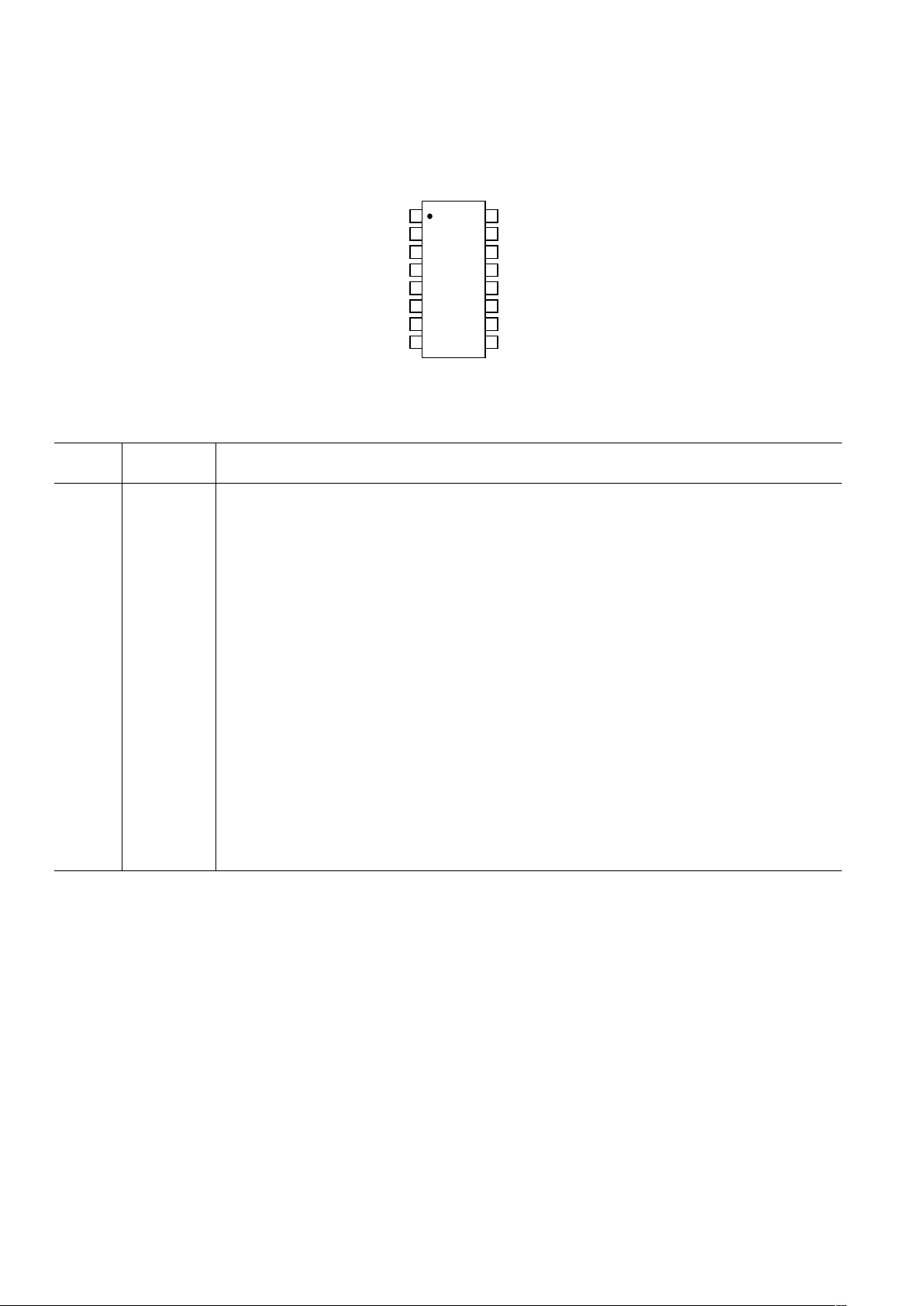
AD5232
PIN FUNCTION DESCRIPTIONS
Pin
Number Mnemonic Description
1 CLK Serial Input Register Clock Pin. Shifts in one bit at a time on positive clock edges.
2 SDI Serial Data Input Pin. MSB Loaded First.
3 SDO Serial Data Output Pin. Open Drain Output requires external pull-up resistor. Commands 9 and 10
activate the SDO output. See Table II. Other commands shift out the previously loaded SDI bit
pattern delayed by 16 clock pulses. This allows daisy-chain operation of multiple packages.
4 GND Ground Pin, Logic Ground Reference.
5V
SS
Negative Supply. Connect to zero volts for single supply applications.
6 A1 A Terminal of RDAC1
7 W1 Wiper Terminal of RDAC1, ADDR(RDAC1) = 0
H
8 B1 B Terminal of RDAC1
9 B2 B Terminal of RDAC2
10 W2 Wiper Terminal of RDAC2, ADDR(RDAC2) = 1
H
11 A2 A Terminal of RDAC2
12 V
DD
Positive Power Supply Pin
13 WP Write Protect Pin. When active low, WP prevents any changes to the present register contents, except
PR and CMD 1 and 8 will refresh RDAC register from EEMEM. Execute a NOP instruction before
returning WP to logic high.
14 PR Hardware Override Preset Pin. Refreshes the scratch pad register with current contents of the EEMEM
register. Factory default loads midscale 80
H
until EEMEM is loaded with a new value by the user
(PR is activated at the logic high transition).
15 CS Serial Register Chip Select Active Low. Serial register operation takes place when CS returns to logic high.
16 RDY Ready. Active-high open drain output, requires pull-up resistor. Identifies completion of commands
2, 3, 8, 9, 10, and PR.
TOP VIEW
(Not to Scale)
16
15
14
13
12
11
10
9
1
2
3
4
5
6
7
8
CLK
SDI
SDO
GND
V
SS
A1
W1
B1
RDY
CS
PR
WP
V
DD
A2
W2
B2
AD5232
PIN CONFIGURATION
Page 7

REV. 0
AD5232
–7–
OPERATIONAL OVERVIEW
The AD5232 digital potentiometer is designed to operate as a
true variable resistor replacement device for analog signals that
remain within the terminal voltage range of V
SS
< V
TERM
< VDD.
The basic voltage range is limited to a |V
DD
– VSS| < 5.5 V. The
digital potentiometer wiper position is determined by the RDAC
register contents. The RDAC register acts as a scratch pad,
register allowing as many value changes as necessary to place the
potentiometer wiper in the correct position. The scratch pad
register can be programmed with any position value using the
standard SPI serial interface mode by loading the complete
representative data word. Once a desirable position is found,
this value can be saved into a corresponding EEMEM
register.
Thereafter the wiper position will always be set at that position
for any future ON-OFF-ON power supply sequence. The
EEMEM save process takes approximately 25 ms, during this
time the shift register is locked preventing any changes from
taking place. The RDY pin indicates the completion of this
EEMEM save.
SCRATCH PAD AND EEMEM PROGRAMMING
The scratch pad register (RDAC register) directly controls the
position of the digital potentiometer wiper. When the scratch
pad register is loaded with all zeros, the wiper will be connected
to the B-Terminal of the variable resistor. When the scratch pad
register is loaded with midscale code (1/2 of full-scale position),
the wiper will be connected to the middle of the variable resistor. And when the scratch pad is loaded with full-scale code, all
1s, the wiper will connect to the A-Terminal. Since the scratch
pad register is a standard logic register, there is no restriction on
the number of changes allowed. The EEMEM registers have a
program erase/write cycle limitation described in the Flash/
EEMEM Reliability section.
BASIC OPERATION
The basic mode of setting the variable resistor wiper position
(programming the scratch pad register) is accomplished by
loading the serial data input register with the command instruction #11, which includes the desired wiper position data. When
the desired wiper position is found, the user loads the serial data
input register with the command instruction #2, which copies
the desired wiper position data into the corresponding nonvolatile EEMEM register. After 25 ms the wiper position will be
permanently stored in the corresponding nonvolatile EEMEM
location. Table I provides an application-programming example
listing the sequence of serial data input (SDI) words and the
corresponding serial data output appearing at the SDO pin in
hexadecimal format.
At system power-on, the scratch pad register is refreshed with
the value last saved in the EEMEM register. The factory preset
EEMEM value is midscale. The scratch pad (wiper) register can
be refreshed with the current contents of the nonvolatile
EEMEM register under hardware control by pulsing the PR pin.
Table I. Set Two Digital POTs to Independent Data Values
then Save Wiper Positions in Corresponding Nonvolatile
EEMEM Registers
SDI SDO Action
B040
H
XXXXHLoads 40H data into RDAC1 register,
Wiper W1 moves to 1/4 full-scale position.
20xx
H
B040
H
Saves copy of RDAC1 register contents
into corresponding EEMEM0 register.
B180
H
20xx
H
Loads 80H data into RDAC2 register,
Wiper W2 moves to 1/2 full-scale position.
21xx
H
B180
H
Saves copy of RDAC2 register contents
into corresponding EEMEM1 register.
Be aware that the PR pulse first sets the wiper at midscale when
brought to logic zero, and then on the positive transition to logic
high, it reloads the DAC wiper register with the contents of
EEMEM. Many additional advanced programming commands
are available to simplify the variable resistor adjustment process.
For example, the wiper position can be changed one step at a
time by using the software-controlled Increment/Decrement
instruction or, by 6 dB at a time, with the Shift Left/Right
instruction command. Once an Increment, Decrement, or Shift
command has been loaded into the shift register, subsequent CS
strobes will repeat this command. This is useful for push-button
control applications. See the Advanced Control Modes description following Table I. A serial data output SDO pin is
available for daisy chaining and for readout of the internal
register contents. The serial input data register uses a 16-bit
[instruction/address/data] WORD.
EEMEM PROTECTION
Write protect (WP) disables any changes of the scratch pad
register contents regardless of the software commands, except
that the EEMEM setting can be refreshed using commands 8
and PR. Therefore, the write-protect (WP) pin provides a hardware EEMEM protection feature. Execute a NOP command
before returning WP to logic high.
DIGITAL INPUT/OUTPUT CONFIGURATION
All digital inputs are ESD-protected high input impedance that
can be driven directly from most digital sources. PR and WP,
which are active at logic low, must be biased to V
DD
if they are
not being used. No internal pull-up resistors are present on any
digital input pins.
The SDO and RDY pins are open-drain digital outputs where
pull-up resistors are needed only if using these functions. A
resistor value in the range of 1 kΩ to 10 kΩ optimizes the power
and switching speed trade-off.
Page 8

REV. 0
–8–
AD5232
SERIAL DATA INTERFACE
The AD5232 contains a 4-wire SPI-compatible digital interface
(SDI, SDO, CS, and CLK), and uses a 16-bit serial data word
loaded MSB first. The format of the SPI-compatible word is
shown in Table II. The chip select (CS) pin needs to be held
low until the complete data word is loaded into the SDI pin.
When CS returns high, the serial data word is decoded according to the instructions in Table III. The Command Bits (Cx)
control the operation of the digital potentiometer. The Address
Bits (Ax) determine which register is activated. The Data Bits
(Dx) are the values that are loaded into the decoded register.
Table IV provides an address map of the EEMEM locations.
The last instruction executed prior to a period of no programming activity should be the No Operation (NOP) instruction.
This will place the internal logic circuitry in a minimum power
dissipation state.
VALID
COMMAND
COUNTER
COMMAND
PROCESSOR
AND ADDRESS
DECODE
SERIAL
REGISTER
CLK
SDI
5V
R
PULLUP
SDO
GND
PR
WP
CS
AD5232
Figure 3. Equivalent Digital Input-Output Logic
The equivalent serial data input and output logic is shown in
Figure 3. The open-drain output SDO is disabled whenever chip
select CS is logic high. The SPI interface can be used in two slave
modes CPHA = 1, CPOL = 1 and CPHA = 0, CPOL = 0.
CPHA and CPOL refer to the control bits, which dictate
SPI timing in these MicroConverters
®
and microprocessors:
ADuC812/ADuC824, M68HC11, and MC68HC16R1/916R1.
ESD protection of the digital inputs is shown in Figures 4a and 4b.
LOGIC
PINS
V
DD
GND
INPUTS
300
AD5232
Figure 4a. Equivalent ESD Digital Input Protection
V
DD
GND
INPUT
300
WP
AD5232
Figure 4b. Equivalent WP Input Protection
DAISY CHAINING OPERATION
The serial data output pin (SDO) serves two purposes. It can
be used to read out the contents of the wiper setting and
EEMEM values usin g in struction 10 and 9 respectively. The
remaining instructions (#0–8, #11–15) are valid for daisychaining multiple devices in simultaneous operations.
Daisy-chaining minimizes the number of port pins required
from the controlling IC (see Figure 5). The SDO pin contains
an open drain N-Channel FET that requires a pull-up resistor if
this function is used. As shown in Figure 5, users need to tie
the SDO pin of one package to the SDI pin of the next
package. Users may need to increase the clock period because
the pull-up resistor and the capacitive loading at the SDO-SDI
interface may require additional time delay between subsequent
packages. If t w o AD5232’s are daisy-chained, 32 bits of data
are required. The first 16 bits go to U 2 and the second 16
bits with the same format go to U1. The 16 bits are formatted
to contain the 4-bit instruction, followed by the 4-bit address,
then the 8 bits of data. The CS should be kept low until all 32
bits are locked into their respective serial registers. The CS
is then pulled high to complete the operation.
SDI SDO
CLK
+V
R
P
2k
C
SDI SDO
CLK
CS CS
U1 U2
AD5232 AD5232
Figure 5. Daisy-Chain Configuration Using SDO
MicroConverter is a registered trademark of Analog Devices, Inc.
Table II. 16-Bit Serial Data Word
MSB B14 B13 B12 B11 B10 B9 B8 B7 B6 B5 B4 B3 B2 B1 LSB
AD5232
C3 C2 C1 C0 A3 A2 A1 A0 D7 D6 D5 D4 D3 D2 D1 D0
Command bits are identified as Cx, address bits are Ax, and data bits are Dx. Command instruction codes are defined
in Table III.
Page 9

REV. 0
AD5232
–9–
Table III. Instruction/Operation Truth Table
Instruction Byte 1 Data Byte 0
Inst B15 B8 B7 B0
No. C3 C2 C1 C0 A3 A2 A1 A0 D7 D6 D5 D4 D3 D2 D1 D0 Operation
0 0000XXXX XX X XXXX X No Operation (NOP). Do nothing.
1 0001000A0 XX X XXXX X Write contents of EEMEM(A0) to
RDAC(A0) Register. This command
leaves device in the Read Program power
state. To return part to the idle state,
perform NOP instruction #0.
2 0010000A0 XX X XXXX X SAVE WIPER SETTING. Write con-
tents of RDAC(ADDR) to EEMEM(A0)
3 0011 << ADDR >> D7 D6 D5 D4 D3 D2 D1 D0 Write contents of Serial Register Data
Byte 0 to EEMEM(ADDR).
4 0100000A0 XXXXXXXX Decrement 6 dB right shift contents of
RDAC(A0), stops at all “Zeros.”
5 0101XXXX XXXXXXXX Decrement All 6 dB right shift contents
of all RDAC Registers, stops at all “Zeros.”
6 0110000A0 XXXXXXXX Decrement contents of RDAC(A0) by
“One,” stops at all “Zeros.”
7 0111XXXX XXXXXXXX Decrement contents of all RDAC Regis-
ters by “One,” stops at all “Zeros.”
8 10000000 XXXXXXXX RESET. Load all RDACs with their cor-
responding EEMEM previously-saved
values.
9 1001 << ADDR >> XXXXXXXX Write contents of EEMEM(ADDR) to
Serial Register Data Byte 0.
10 1010000A0 XXXXXXXX Write contents of RDAC(A0) to Serial
Register Data Byte 0.
11 1011000A0 D7D6D5D4D3D2D1D0 Write contents of Serial Register Data
Byte 0 to RDAC(A0).
12 1100000A0 XXXXXXXX Increment 6 dB left shift contents of
RDAC(A0), stops at all “Ones.”
13 1101XXXX XXXXXXXX Increment all 6 dB left shift contents
of all RDAC Registers, stops at all “Ones.”
14 1110000A0 XXXXXXXX Increment contents of RDAC(A0) by
“One,” stops at all “Ones.”
15 1111XXXX XXXXXXXX Increment contents of all RDAC Regis-
ters “One,” stops at all “Ones.”
NOTES
1. The SDO output shifts out the last eight bits of data clocked into the serial register for daisy-chain operation. Exception: following Instruction #9 or #10 the selected internal
register data will be present in data byte 0. Instructions following #9 and #10 must be a full 16-bit data word to completely clock out the contents of the serial register.
2. The RDAC register is a volatile scratch pad register that is refreshed at power-on from the corresponding nonvolatile EEMEM register.
3. The increment, decrement, and shift commands ignore the contents of the shift register Data Byte 0.
4. Execution of the Operation column noted in the table takes place when the CS strobe returns to logic high.
5. Execution of a NOP instruction minimizes power dissipation.
Page 10

REV. 0
–10–
AD5232
Also the left shift commands were modified so that if the data in
the RDAC register is greater than or equal to midscale and the
data is left shifted then the data in the RDAC register is set to
full-scale. This makes the left shift function as close to ideally
logarithmic as is possible.
The right shift #4 and #5 commands will be ideal only if the
LSB is zero (i.e., ideal logarithmic–no error). If the LSB is a
one then the right shift function generates a linear half LSB
error, which translates to a code dependent logarithmic error
for odd codes only as shown in the attached plots, (see Figure
5). The plot shows the errors of the odd codes for the AD5232.
0000 0000
0000 0001
0000 0010
0000 0100
0000 1000
0001 0000
0010 0000
0100 0000
1000 0000
1111 1111
1111 1111
LEFT SHIFT
1111 1111
0111 1111
0011 1111
0001 1111
0000 1111
0000 0111
0000 0011
0000 0001
0000 0000
0000 0000
0000 0000
RIGHT SHIFT
LEFT
SHIFT
(+6 dB)
RIGHT
SHIFT
(–6 dB)
Figure 6. Detail Left and Right Shift Function for the
8-Bit AD5232
Actual conformance to a logarithmic curve between the data
contents in the RDAC register and the wiper position for each
Right Shift #4 and #5 command execution contains an error
only for the odd codes. Even codes are ideal except zero right
shift or greater than half-scale left shift. The graph in Figure 7
shows plots of Log_Error [i.e., 20 × log 10 (error/code)]. For
example, code 3 Log_Error = 20 × log 10 (0.5/3) = –15.56 dB,
which is the worst case. The plot of Log_Error is more significant at the lower codes.
CODE, FROM 1 TO 255 BY 2
20 40 60 80 100 0 120
140
160 180 200 220 240 260
0
–10
–20
–30
–40
–50
–60
dB
LOG_ERROR (CODE) FOR 8-BIT
Figure 7. Plot of Log_Error Conformance for Odd Codes
Only (Even Codes Are Ideal)
ADVANCED CONTROL MODES
The AD5232 digital potentiometer contains a set of user programming features to address the wide applications available to these
universal adjustment devices. Key programming features include:
Independently Programmable Read and Write to all registers.
• Simultaneous refresh of all RDAC wiper registers from
corresponding internal EEMEM registers.
•
Increment and Decrement instructions for each RDAC wiper
register.
• Left and right bit shift of all RDAC wiper registers to achieve
6 dB level changes.
• Nonvolatile storage of the present scratch pad RDAC register
values into the corresponding EEMEM register.
• Fourteen extra bytes of user-addressable electrical-erasable memory.
Increment and Decrement Commands
The increment and decrement commands (#14, #15, #6, #7)
are useful for the basic servo adjustment application. This command simplifies microcontroller software coding by eliminating
the need to perform a readback of the current wiper position,
then add one to the register contents using the microcontroller’s
adder. The microcontroller simply sends an increment command
(#14) to the digital POT, which will automatically move the
wiper to the next resistance segment position. The master increment command (#15) will move all POT wipers by one position
from their present position to the next resistor segment position.
The direction of movement is referenced to Terminal B. Thus
each increment #15 command will move the wiper tap position
farther away from Terminal B.
Logarithmic Taper Mode Adjustment
Programming instructions allow a decrement and an increment
wiper position control by individual POT or in a ganged POT
arrangement where both wiper positions are changed at the
same time. These settings are activated by the 6 dB decrement
and 6 dB increment instructions #4 and #5 and #12 and #13
respectively. For example, starting with the wiper connected to
Terminal B executing nine increment instructions (#12) would
move the wiper in +6 dB steps from the 0% of R
BA
(B terminal)
position to the 100% of R
BA
position of the AD5232 8-Bit
potentiometer. The 6 dB increment instruction doubles the
value of the RDAC register contents each time the command is
executed. When the wiper position is greater than midscale, the
last 6 dB increment instruction will cause the wiper to go to the
Full-Scale 255 code position. Any additional +6 dB instruction
will no longer change the wiper position from full scale (RDAC
register code = 255).
Figure 6 illustrates the operation of the 6 dB shifting function
on the individual RDAC register data bits for the 8-bit AD5232
example. Each line going down the table represents a successive
shift operation. Very important: the left shift #12 and #13 commands were modified so that if the data in the RDAC register is
equal to zero and the data is left shifted, it is then set to code 1.
Page 11

REV. 0
AD5232
–11–
USING ADDITIONAL INTERNAL NONVOLATILE EEMEM
The AD5232 contains additional internal user storage registers
(EEMEM) for saving constants and other 8-bit data. Table IV
provides an address map of the internal nonvolatile storage
registers shown in the functional block diagram as EEMEM1,
EEMEM2, and bytes of USER EEMEM.
Table IV. EEMEM Address Map
EEMEM EEMEM Contents of Each
Address Device EEMEM (ADDR)
(ADDR) AD5232 (8B)
0000 RDAC1
0001 RDAC2
0010 USER 1
0011 USER 2
0100 USER 3
0101 USER 4
*** ***
1111 USER 14
NOTES
1
RDAC data stored in EEMEM locations are transferred to their
corresponding RDAC REGISTER at Power ON, or when
instructions Inst#1 and Inst#8 are executed.
2
USER <data> is internal nonvolatile EEMEM registers available
to store and retrieve constants using Inst#3 and Inst#9 respectively.
3
AD5232 EEMEM locations are 1 byte each (8 bits).
4
Execution of instruction #1 leaves the device in the Read Mode power consumption state. After the last Instruction #1 is executed, the user should
perform a NOP, Instruction #0 com mand to return the device to the low
power idle state.
V
DD
A
W
B
V
SS
Figure 8. Maximum Terminal Voltages Set by VDD and V
SS
DETAIL POTENTIOMETER OPERATION
The actual structure of the RDAC is designed to emulate the
performance of a mechanical potentiometer. The patent-pending
RDAC contains multiple strings of connected resistor segments,
with an array of analog switches that act as the wiper connection
to several points along the resistor array. The number of points
is the resolution of the device. For example, the AD5232 has
256 connection points allowing it to provide better than 0.5%
setability resolution. Figure 9 provides an equivalent diagram of the connections between the three terminals that
make up one channel of the RDAC. The SW
A
and SWB will
always be ON, while one of the switches SW(0) to SW(2
N
–1)
will be ON one at a time depending upon the resistance step
decoded from the Data Bits. The resistance contributed by R
W
must be accounted for in the output resistance. The SWA and
SW
B
will always be ON while one of the switches SW(0) to
SW(2
N
–1) will be ON one at a time, depending upon the
resistance step decoded from the Data Bits. The resistance
contributed by R
W
must be accounted for in the output resistance.
SW
A
SW(2
N
–
1)
A
X
W
X
SW(2
N
–
2)
SW
(1)
SW
(0)
SW
B
B
X
RDAC
WIPER
REGISTER
AND
DECODER
R
S = RAB
/2
N
R
S
R
S
R
S
DIGITAL
CIRCUITRY
OMITTED FOR
CLARITY
Figure 9. Equivalent RDAC Structure (Patent Pending)
Table V. RDAC and Digital Register Address Map
Register Address Name of Register*
(ADDR) AD5232 (8B)
0000 RDAC1
0001 RDAC2
*RDACx registers contain data determining the
position of the variable resistor wiper.
TERMINAL VOLTAGE OPERATING RANGE
The digital potentiometer’s positive VDD and negative VSS power
supply defines the boundary conditions for proper three-terminal
programmable resistance operation. Signals present on terminals
A, B, W that exceed V
DD
or VSS will be clamped by a forward
biased diode; see Figure 8.
The ground pin of the AD5232 device is primarily used as a
digital ground reference, which needs to be tied to the PCBs’
common ground. The digital input logic signals to the AD5232
must be referenced to the devices’ ground pin (GND), and
satisfy the logic minimum input high level and the maximum
low level defined in the specification table of this data sheet.
An internal level-shift circuit between the digital interface and
the wiper switch control ensures that the common-mode voltage
range of the three-terminals A, W, and B extends from V
SS
to VDD.
Page 12

REV. 0
–12–
AD5232
Table VI. Nominal Individual Segment Resistor Values ()
Segment Resistor Size
for R
AB
End-to-End Values
10 k Version 50 k Version 100 k Version
8-Bit 78.10 390.5 781.0
PROGRAMMING THE VARIABLE RESISTOR
Rheostat Operation
The nominal resistances of the RDAC between terminals A and B
are available with values of 10 kΩ, 50 kΩ, and 100 kΩ. The final
digits of the part number determine the nominal resistance value,
e.g., 10 kΩ = 10; 100 kΩ = 100. The nominal resistance (R
AB
) of
the AD5232 VR has 256 contact points accessed by the wiper
terminal, plus the B terminal contact. The 8-bit data word in the
RDAC latch is decoded to select one of the 256 possible settings.
The general transfer equation, which determines the digitally
programmed output resistance between Wx and Bx, is:
R
WB
(Dx) = (Dx)/2N × RBA + R
W
(1)
Where N is the resolution of the VR, Dx is the data contained in
the RDACx latch, and R
BA
is the nominal end-to-end resistance.
For example, the following output resistance values will be set
for the following RDAC latch codes (applies to the 8-bit, 10 kΩ
potentiometers):
Table VII. Nominal Resistance Value at Selected Codes for
R
AB
= 10 k
D (DEC) R
WB
(V) Output State
255 10011 Full-Scale
128 5050 Midscale
1891 LSB
0 50 Zero-Scale*(Wiper Contact Resistance)
*Note that in the zero-scale condition a finite wiper resistance of 50 Ω is present. Care
should be taken to limit the current flow between W and B in this state to a
maximum continuous value of 2 mA to avoid degradation or possible de struction of the internal switch metalization. Intermittent current operation to
20 mA is allowed.
CODE – Decimal
100
75
0
0 25664
PERCENT OF NOMINAL
END-TO-END RESISTANCE – % R
AB
128 192
50
25
R
WB
R
WA
Figure 10. Symmetrical RDAC Operation
Like the mechanical potentiometer the RDAC replaces, the
AD5232 parts are totally symmetrical. The resistance between
the wiper W and terminal A also produces a digitally controlled
resistance R
WA
. Figure 10 shows the symmetrical programmability of the various terminal connections. When these terminals
are used the B–terminal should be tied to the wiper. Setting the
resistance value for R
WA
starts at a maximum value of resistance
and decreases as the data loaded in the latch is increased in
value. The general transfer equation for this operation is:
R
WA
(Dx) = (2N-Dx)/2N × RBA + R
W
(2)
where N is the resolution of the VR, Dx is the data contained in
the RDACx latch, and R
BA
is the nominal end-to-end resistance.
For example, the following output resistance values will be set
for the following RDAC latch codes (applies to 8-bit, 10 kΩ
potentiometers).
Table VIII. Nominal Resistance Value at Selected
Codes for R
AB
= 10 k
D (DEC) R
WA
(W) Output State
255 89 Full-Scale
128 5050 Midscale
1 10011 1 LSB
0 10050 Zero-Scale
The multichannel AD5232 has a ±0.2% typical distribution of
internal channel-to-channel R
BA
match. Device-to-device
matching is process-lot-dependent and exhibits a –40% to +20%
variation. The change in R
BA
with temperature has a 600 ppm/°C
temperature coefficient.
Device
Resolution
Page 13

REV. 0
AD5232
–13–
PROGRAMMING THE POTENTIOMETER DIVIDER
Voltage Output Operation
The digital potentiometer easily generates an output voltage
proportional to the input voltage applied to a given terminal.
For example, connecting A-terminal to 5 V and B-terminal to
ground produces an output voltage at the wiper which can be
any value starting at zero volts up to 5 V. Each LSB of voltage is
equal to the voltage applied across terminal AB divided by the
2
N
position resolution of the potentiometer divider. The general
equation defining the output voltage with respect to ground for
any given input voltage applied to terminals AB is:
V
W
(Dx) = Dx/2N × VAB + V
B
(3)
Operation of the digital potentiometer in the divider mode results in
more accurate operation over temperature. Here the output voltage is
dependent on the ratio of the internal resistors, not the absolute
value; therefore, the drift improves to 15 ppm/°C. There is no
voltage polarity restriction between terminals A, B, and W, as long
as the terminal voltage (V
TERM
) stays within VSS < V
TERM
< VDD.
OPERATION FROM DUAL SUPPLIES
The AD5232 can be operated from dual supplies enabling control of ground-referenced ac signals. See Figure 11 for a typical
circuit connection.
~
2V p-p
AD5232
V
SS
GND
SDI
CLK
SS
SCLK
MOSI
GND
V
DD
C
1V p-p
V
DD
+2.75V
–2.5V
CS
Figure 11. Operation from Dual Supplies
C
A
AB
C
B
C
W
RDAC
10k
W
60pF
C
A
= 45pF CB = 45pF
Figure 12. RDAC Circuit Simulation Model for RDAC = 10 k
Ω
The internal parasitic capacitances and the external capacitive loads
dominate the ac characteristics of the RDACs. Configured as a
potentiometer divider the –3 dB bandwidth of the AD5232BRU10
(10 kΩ resistor) measures 500 kHz at half scale. Figure TPC 10
provides the large signal BODE plot characteristics of the three
resistor versions 10 kΩ, 50 kΩ, and 100 kΩ. A parasitic simulation model has been developed, and is shown in Figure 12.
Listing I provides a macro model net list for the 10 kΩ RDAC:
Listing I. Macro Model Net List for RDAC
.PARAM DW=255, RDAC=10E3
*
.SUBCKT DPOT (A,W,B)
*
CA A 0 {45E-12}
RAW A W {(1-DW/256)*RDAC+50}
CW W 0 60E-12
RBW W B {DW/256*RDAC+50}
CB B 0 {45E-12}
*
.ENDS DPOT
APPLICATION PROGRAMMING EXAMPLES
The following command sequence examples have been developed
to illustrate a typical sequence of events for the various features
of the AD5232 nonvolatile digital potentiometer.
[PCB = Printed Circuit Board containing the AD523x part].
Instruction numbers (Commands), addresses and data appearing at SDI and SDO pins are listed in hexadecimal.
Table IX. Set Two Digital POTs to Independent Data Values
SDI SDO Action
B140
H
XXXX
H
Loads 40H data into RDAC2 register,
Wiper W2 moves to 1/4 full-scale
position.
B080
H
B140
H
Loads 80H data into RDAC1 register,
Wiper W1 moves to 1/2 Full-Scale
position.
Page 14

REV. 0
–14–
AD5232
Table X. Active Trimming of One POT Followed by a Save to
Nonvolatile Memory (PCB Calibrate)
SDI SDO Action
B040
H
XXXXHLoads 40H data into RDAC1 register,
Wiper W1 moves to 1/4 full-scale
position.
E0XX
H
B040
H
Increments RDAC1 register by one to
41
H
, Wiper W1 moves one resistor
segment away from terminal B.
E0XX
H
E0XX
H
Increments RDAC1 register by one to
42
H
, Wiper W1 moves one more
resistor segment away from terminal B.
Continue until desired wiper position
reached.
20XX
H
E0XX
H
Saves RDAC1 register data into
corresponding nonvolatile EEMEM1
memory ADDR = 0H.
EQUIPMENT CUSTOMER STARTUP SEQUENCE FOR A
PCB CALIBRATED UNIT WITH PROTECTED SETTINGS
PCB setting: Tie WP to GND [prevents changes in PCB
wiper set position]
Power V
DD
and V
SS
with respect to GND
Optional: Strobe PR pin [ensures full power ON preset of
wiper register with EEMEM contents in unpredictable supply
sequencing environments]
Table XI. Using Left Shift by One to Change Circuit Gain in
6 dB Steps
SDI SDO Action
C1XXHXXXXHMoves Wiper W2 to double the present
data value contained in RDAC2 register, in the direction of the A terminal.
C1XX
H
XXXXHMoves Wiper W2 to double the present
data value contained in RDAC2 register, in the direction of the A terminal.
Table XII. Storing Additional Data in Nonvolatile Memory
SDI SDO Action
3280
H
XXXXHStores 80H data into spare EEMEM
location USER1.
3340
H
XXXXHStores 40H data into spare EEMEM
location USER2.
Table XIII. Reading Back Data from Various Memory Locations
SDI SDO Action
94XX
H
XXXXHPrepares data read from USER3 location.
Assumption: USER3 previously loaded
with 80
H
.
00XX
H
XX80
H
NOP instruction #0 sends 16-bit word
out of SDO where the last 8 bits contain the contents of USER3 location.
NOP command ensures device returns
to idle power dissipation state.
Analog Devices offers the AD5232EVAL board for sale to
simplify evaluation of these programmable devices controlled by
a personal computer via the printer port.
TEST CIRCUITS
Figures 13 to 22 define the test conditions used in the product
specification’s table.
A
W
B
NC
I
W
DUT
V
MS
NC = NO CONNECT
Figure 13. Resistor Position Nonlinearity Error (Rheostat
Operation; R-INL, R-DNL)
A
W
B
DUT
V
MS
V+
V+ = V
DD
1LSB = V+/2
N
Figure 14. Potentiometer Divider Nonlinearity Error Test
Circuit (INL, DNL)
A
W
B
DUT
I
W
V
MS1
V
MS2
V
W
R
W
=
[
V
MS1
– V
MS2
]
/I
W
Figure 15. Wiper Resistance Test Circuit
A
W
B
V
MS
V+ = V
DD
10%
PSRR (dB) = 20 LOG
V
MS
V
DD
(
)
~
V
A
V
DD
V
MS
%
V
DD
%
PSS (%/%) =
V+
Figure 16. Power Supply Sensitivity Test Circuit (PSS, PSRR)
~
OFFSET BIAS
OFFSET
GND
ABDUT
W
5V
V
IN
V
OUT
OP279
Figure 17. Inverting Gain Test Circuit
Page 15

REV. 0
AD5232
–15–
~
OFFSET BIAS
OFFSET
GND
ABDUT
W
5V
V
IN
V
OUT
OP279
Figure 18. Noninverting Gain Test Circuit
~
OFFSET
GND
A
B
DUT
W
+15V
V
IN
V
OUT
OP42
–15V
2.5V
Figure 19. Gain vs. Frequency Test Circuit
+
_
DUT
CODE = OO
H
0.1V
V
SS
TO V
DD
R
SW
=
0.1V
I
SW
ISW
W
B
Figure 20. Incremental ON Resistance Test Circuit
DUT
V
SS
ICM
W
B
V
DD
NC
NC
V
CM
GND
A
NC = NO CONNECT
Figure 21. Common-Mode Leakage Current Test Circuit
W2
B2
V
DD
A2
~
V
IN
NC
W1
RDAC
1
A1
B1
V
SS
V
OUT
RDAC
2
C
= 20 log [V
/V
]
Figure 22. Analog Crosstalk Test Circuit
Flash/EEMEM Reliability
The Flash/EE Memory array on the AD5232 is fully qualified
for two key Flash/EE memory characteristics, namely Flash/EE
Memory Cycling Endurance and Flash/EE Memory Data
Retention.
Endurance quantifies the ability of the Flash/EE memory to be
cycled through many Program, Read, and Erase cycles. In real
terms, a single endurance cycle is composed of four independent, sequential events. These events are defined as:
a. Initial page erase sequence
b. Read/verify sequence
c. Byte program sequence
d. Second read/verify sequence
During reliability qualification Flash/EE memory is cycled from
00
H
to FFH until a first fail is recorded, signifying the endurance
limit of the on-chip Flash/EE memory.
As indicated in the specification pages of this data sheet, the
AD5232 Flash/EE Memory Endurance qualification has been
carried out in accordance with JEDEC Specification A117 over
the industrial temperature range of –40°C to +85°C. The results
allow the specification of a minimum endurance figure over supply
and temperature of 100,000 cycles, with an endurance figure of
700,000 cycles being typical of operation at 25°C.
Retention quantifies the ability of the Flash/EE memory to retain
its programmed data over time. Again, the AD5232 has been
qualified in accordance with the formal JEDEC Retention Lifetime Specification (A117) at a specific junction temperature
(T
J
= 55°C). As part of this qualification procedure, the Flash/EE
memory is cycled to its specified endurance limit described above,
before data retention is characterized. This means that the Flash/EE
memory is guaranteed to retain its data for its full-specified retention lifetime every time the Flash/EE memory is reprogrammed. It
should also be noted that retention lifetime, based on an activation energy of 0.6 eV, will derate with T
J
as shown in Figure 23.
T
J
JUNCTION TEMPERA TURE – C
300
250
0
40
RETENTION – Y ears
200
150
100
50
50 60 70 80 90 100 110
ADI TYPICAL
PERFORMANCE
AT
T
J
= 55C
Figure 23. Flash/EE Memory Data Retention
Page 16

REV. 0
–16–
AD5232
DIGITAL CODE
2.00
–0.50
–2.00
0
IINL ERROR – LSB
1.50
0
–1.00
–1.50
1.00
0.50
64 128 192
1.75
1.25
0.75
–0.25
–0.75
–1.25
–1.75
0.25
INL TA = –40C
INL TA = +85C
INL TA = +25C
256
V
DD
= 2.7V
VSS = 0V
TPC 1. INL vs. Code, TA = –40⬚C, +25⬚C, +85⬚C Overlay
DIGITAL CODE
2.00
–0.50
–2.00
1
DNL ERROR – LSB
1.50
0
–1.00
–1.50
1.00
0.50
64 128 192
1.75
1.25
0.75
–0.25
–0.75
–1.25
–1.75
0.25
DNL TA = –40C
DNL TA = +25C
DNL TA = +85C
256
V
DD
= 2.7V
V
SS
= 0V
TPC 2. DNL vs. Code, TA = –40⬚C, +25⬚C, +85⬚C Overlay
CODE – Decimal
0.20
–0.20
0
32
64
96
128
0.15
0.00
–0.05
–0.10
–0.15
0.10
0.05
160 192 224 256
V
DD
= 5.5V, V
SS
= 0V
T
A
= 25C
R-DNL – LSB
TPC 3. R-DNL vs. Code RAB = 10 kΩ, 50 kΩ, 100 kΩ Overlay
2000
0
032
RHEOSTAT MODE TEMPCO – ppm/C
64 96 128
160
1000
500
1500
192 224 256
CODE – Decimal
TA = –40C/+85C
V
A
= NO CONNECT
R
WB
MEASURED
V
DD
= 5V
TPC 4. ∆RWB/∆T vs. Code RAB = 10 kΩ, VDD = 5 V
70
032
POTENTIOMETER MODE TEMPCO – ppm/C
64 96 128
160 192 224 256
VDD = 5V
T
A
= –40C/+85C
V
A
= 2.00V
V
B
= 0V
–10
60
30
20
10
0
50
40
CODE – Decimal
TPC 5. ∆VWB/∆T vs. Code RAB = 10 kΩ, VDD = 5 V
0.001
–50 –35
I
CM
– A
–20 –510
25
0.01
40 55 70
TEMPERATURE – C
0.1
1
85
VDD = +2.5V
V
CM
= 0V
V
SS
= –2.5V
SEE FIGURE 21
TPC 6. ICM vs. Temperature
–T ypical Performance Characteristics
Page 17

REV. 0
AD5232
–17–
–50 –35
I
DD
–
A
–20 –510
25240 55 70
TEMPERATURE – C
4
85
VDD = 5.5V
VDD = 2.7V
TPC 7. IDD vs. Temperature
TPC 8. IDD vs. Time (Save) Program Mode
FREQUENCY – Hz
12
6
–42
1k 10k
GAIN – dB
0
–6
–30
–12
–18
–24
–36
100k 1M
f
–3dB
= 500kHz, R = 10k
VIN = 100mV rms
V
DD
= +2.5V, V
SS
= –2.5V
R
L
= 1M
f
–3dB
= 45kHz, R = 100k
f
–
3dB
= 95kHz, R = 50k
TA = 25C
TPC 10. –3 dB Bandwidth vs. Resistance
FREQUENCY – Hz
10
10
THD + NOISE – %
1
0.1
0.01
0.001
100 1k 10k 100k
RAB = 10k
RAB = 50k, 100k
TA = 25C
VDD = 5V
FILTER = 22kHz
TPC 11. Total Harmonic Distortion vs. Frequency
CODE
0
1
R
w
–
64 128 192
10
20
30
40
50
60
70
80
90
100
110
256
TA = 25C
V
DD
= 2.7V
TPC 12. Wiper On-Resistance vs. Code
TPC 9. I
DD
vs. Time Read Mode
Page 18

REV. 0
–18–
AD5232
FREQUENCY– Hz
0
–60
1k
GAIN – dB
–30
100k10k
–6
–36
–42
–48
–54
–24
–12
–18
1M
VDD = +2.7V
V
SS
= –2.7V
V
A
= 100mV rms
T
A
= 25C
V
A
DATA = 80
H
DATA = 40
H
DATA = 20
H
DATA = 10
H
DATA = 08
H
DATA = 04
H
DATA = 02
H
DATA = 01
H
R
AB
= 10k
TPC 13. Gain vs. Frequency vs. Code, R
AB
= 10 k
Ω
FREQUENCY – Hz
0
–60
1k
GAIN – dB
–30
100k10k
–6
–36
–42
–48
–54
–24
–12
–18
1M
VDD = +2.7V
V
SS
= –2.7V
V
A
= 100mV rms
T
A
= 25C
V
A
DATA = 80
H
DATA = 40
H
DATA = 20
H
DATA = 10
H
DATA = 08
H
DATA = 04
H
DATA = 02
H
DATA = 01
H
RAB = 50k
TPC 14. Gain vs. Frequency vs. Code, R
AB
= 50 k
Ω
FREQUENCY – Hz
0
–60
1k
GAIN – dB
–30
100k10k
–6
–36
–42
–48
–54
–24
–12
–18
1M
VDD = +2.7V
V
SS
= –2.7V
V
A
= 100mV rms
T
A
= 25C
V
A
DATA = 80
H
DATA = 40
H
DATA = 20
H
DATA = 10
H
DATA = 08
H
DATA = 04
H
DATA = 02
H
DATA = 01
H
RAB = 100k
TPC 15. Gain vs. Frequency vs. Code, R
AB
= 100 k
Ω
FREQUENCY – Hz
80
0
1k
PSRR REJECTION – dB
40
100k10k
20
1M
60
TA = 25C
V
DD
= 5.5V 100mV ac
V
SS
= 0V, VB = 5V, VA = 0V
MEASURE at V
W
WITH CODE = 80
H
RAB = 100k
RAB = 50k
RAB = 10k
TPC 16. PSRR vs. Frequency
FREQUENCY – kHz
120
20
1
C
TA
ANALOG CROSSTALK REJECTION – dB
60
10
40
100
80
VDD = VA2 = +2.75V
V
SS
= VB2 = –2.75V
V
IN
= +2.5V
P
RAB = 100k
RAB = 50k
RAB = 10k
SEE TEST CIRCUIT, FIGURE 22
100
TA = 25C
TPC 17. Analog Crosstalk vs. Frequency
Page 19

REV. 0
AD5232
–19–
Number Resolution Power
of VRs Terminal Interface Nominal (Number Supply
Part per Voltage Data Resistance of Wiper Current
Number Package Range (V) Control (k) Positions) (I
DD
)(A) Packages Comments
AD5201 1 ±3, +5.5 3-wire 10, 50 33 40 µSOIC-10 Full ac Specs, Dual
Supply, Pwr-On-Reset,
Low Cost
AD5220 1 5.5 UP/ 10, 50, 100 128 40 PDIP, SO-8, No Rollover,
DOWN µSOIC-8 Pwr-On-Reset
AD7376 1 ±15 , +28 3-wire 10, 50, 100, 1000 128 100 PDIP-14, Single 28 V
SOL-16, or Dual ±15 V
TSSOP-14 Supply Operation
AD5200 1 ±3 , +5.5 3-wire 10, 50 256 40 µSOIC-10 Full ac Specs,
Dual Supply,
Pwr-On-Reset
AD8400 1 5.5 3-wire 1, 10, 50, 100 256 5 SO-8 Full ac Specs
AD5260 1 ±5, +15 3-wire 20, 50, 200 256 60 TSSOP-14 +5 V to+15 V or ±5 V
Operation,
TC < 50 ppm/°C
AD5241 1 ±3, +5.5 2-wire 10, 100, 1000 256 50 SO-14, I
2
C Compatible,
TSSOP-14 TC < 50 ppm/°C
AD5231 1 ±2.75, +5.5 3-wire 10, 50, 100 1024 10 TSSOP-16 Nonvolatile Memory,
Direct Program, I/D,
±6 dB Settability
AD5222 2 ±3, +5.5 UP/ 10, 50, 100, 1000 128 80 SO-14, No Rollover, Stereo,
DOWN TSSOP-14 Pwr-On-Reset,
TC < 50 ppm/°C
AD8402 2 5.5 3-wire 1, 10, 50, 100 256 5 PDIP, SO-14, Full ac Specs, nA
TSSOP-14 Shutdown Current
AD5207 2 ±3, +5.5 3-wire 10, 50, 100 256 40 TSSOP-14 Full ac Specs, Dual
Supply, Pwr-OnReset, SDO
AD5232 2 ±2.75, +5.5 3-wire 10, 50, 100 256 10 TSSOP-16 Nonvolatile Memory,
Direct Program, I/D,
±6 dB Settability
AD5235* 2 ±2.75, +5.5 3-wire 25, 250 1024 20 TSSOP-16 Nonvolatile Memory,
Direct Program,
TC < 50 ppm/°C
AD5242 2 ±3, +5.5 2-wire 10, 100, 1000 256 50 SO-16, I
2
C Compatible,
TSSOP-16 TC < 50 ppm/°C
AD5262* 2 ±5, +15 3-wire 20, 50, 200 256 60 TSSOP-16 +5 V to +15 V or ±5 V
Operation,
TC < 50 ppm/°C
AD5203 4 5.5 3-wire 10, 100 64 5 PDIP, SOL-24, Full ac Specs, nA
TSSOP-24 Shutdown Current
AD5233 4 ±2.75, +5.5 3-wire 10, 50, 100 64 10 TSSOP-16 Nonvolatile Memory,
Direct Program,
I/D, ±6 dB Settability
AD5204 4 ±3, +5.5 3-wire 10, 50, 100 256 60 PDIP, SOL-24, Full ac Specs,
TSSOP-24 Dual Supply,
Pwr-On-Reset
AD8403 4 5.5 3-wire 1, 10, 50, 100 256 5 PDIP, SOL-24, Full ac Specs, nA
TSSOP-24 Shutdown Current
AD5206 6 ±3, +5.5 3-wire 10, 50, 100 256 60 PDIP, SOL-24, Full ac Specs,
TSSOP-24 Dual Supply,
Pwr-On-Reset
*Future Product, consult factory for latest status.
Latest Digital Potentiometer Information located at: www.analog.com/DigitalPotentiometers
DIGITAL POTENTIOMETER FAMILY SELECTION GUIDE
Page 20

REV. 0
–20–
C02618–1–10/01(0)
PRINTED IN U.S.A.
AD5232
OUTLINE DIMENSIONS
Dimensions shown in inches and (mm).
PRINTED IN U.S.A.
16-Lead TSSOP
(RU-16)
16
9
81
0.256 (6.50)
0.246 (6.25)
0.177 (4.50)
0.169 (4.30)
PIN 1
0.201 (5.10)
0.193 (4.90)
SEATING
PLANE
0.006 (0.15)
0.002 (0.05)
0.0118 (0.30)
0.0075 (0.19)
0.0256 (0.65)
BSC
0.0433 (1.10)
MAX
0.0079 (0.20)
0.0035 (0.090)
0.028 (0.70)
0.020 (0.50)
8
0
 Loading...