

Page 1
32-Position Manual Up/Down Control
FEATURES
32-position digital potentiometer
10 kΩ, 50 kΩ, 100 kΩ end-to-end terminal resistance
Simple manual up/down control
Self-contained, requires only 2 pushbutton tactile switches
Built-in adaptive debouncer
Discrete step-up/step-down control
Autoscan up/down control with 4 steps per second
Pin-selectable zero-scale/midscale preset
Low potentiometer mode tempco, 5 ppm/°C
Low rheostat mode tempco, 35 ppm/°C
Digital control compatible
Ultralow power, I
Low operating voltage, 2.7 V to 5.5 V
Automotive temperature range, −40°C to +105°C
Compact thin SOT-23-8 (2.9 mm × 3 mm) Pb-free package
APPLICATIONS
Mechanical potentiometer and trimmer replacements
LCD backlight, contrast, and brightness controls
Digital volume control
Portable device-level adjustments
Electronic front panel-level controls
Programmable power supply
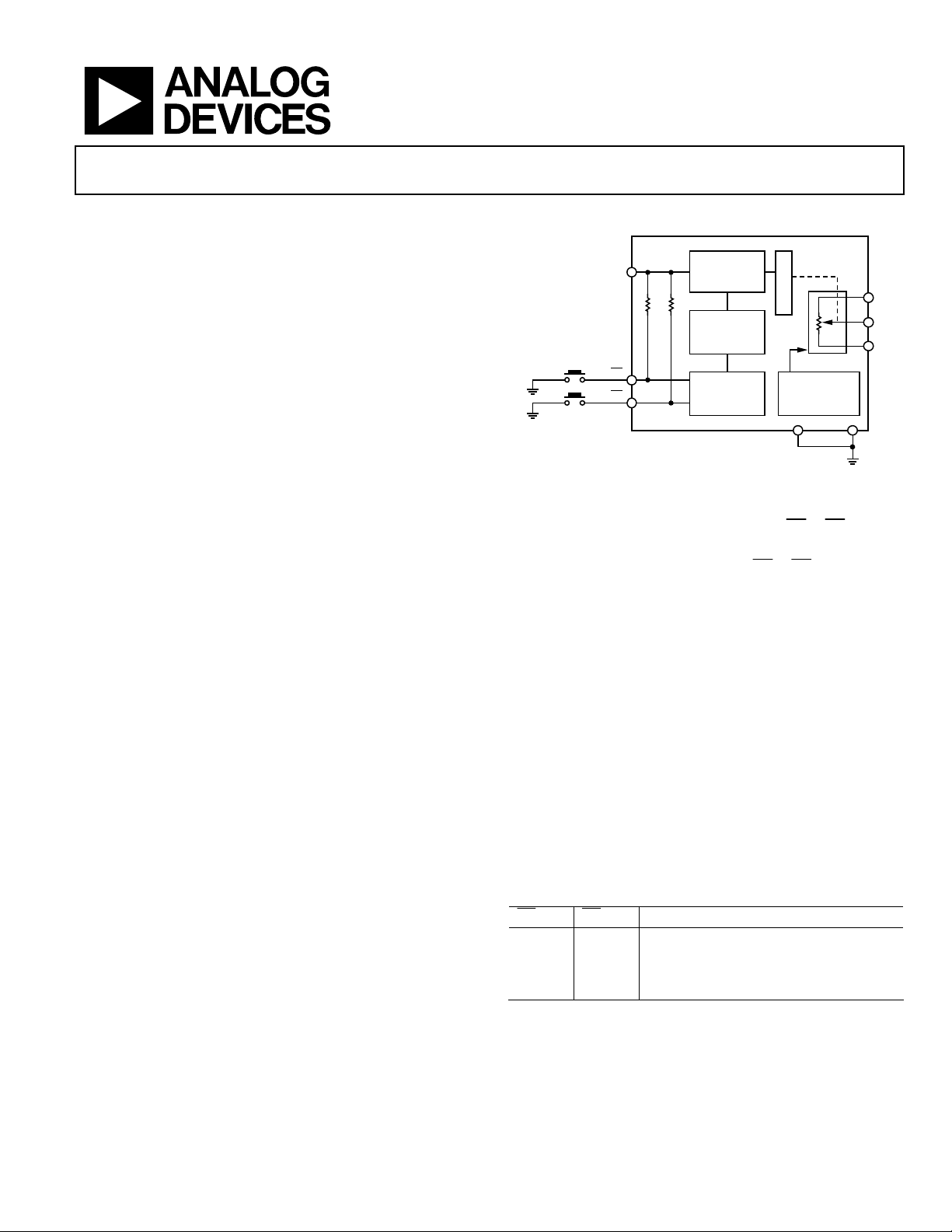
GENERAL DESCRIPTION
The AD5228 is Analog Devices’ latest 32-step-up/step-down
control digital potentiometer emulating mechanical potentiometer operation
manual control with just two external pushbutton tactile
switches. The AD5228 is designed with a built-in adaptive
debouncer that ignores invalid bounces due to contact bounce
commonly found in mechanical switches. The debouncer is
adaptive, accommodating a variety of pushbutton tactile
switches that generally have less than 10 ms of bounce time
during contact closures. When choosing the switch, the user
should consult the timing specification of the switch to ensure
its suitability in an AD5228 application.
1
The term s digital potentiometer and RDAC are used interchangeably.
= 0.4 µA typ and 3 µA max
DD
1
. Its simple up/down control interface allows
Potentiometer
AD5228
FUNCTIONAL BLOCK DIAGRAM
D
UP/DOWN
CONTROL
LOGIC
DISCRETE
STEP/AUTO
SCAN DETECT
ADAPTIVE
DEBOUNCER
Figure 1.
PUSH-UP
BUTTON
PUSH-DOWN
BUTTON
V
DD
R1 R2
PU
PD
The AD5228 can increment or decrement the resistance in
discrete steps or in autoscan mode. When the
is pressed briefly (no longer than 0.6 s), the resistance of the
AD5228 changes by one step. When the
PU
continuously for more than a second, the device activates the
autoscan mode and changes four resistance steps per second.
The AD5228 can also be controlled digitally; its up/down
features simplify microcontroller usage. The AD5228 is available
in a compact thin SOT-23-8 (TSOT-8) package. The part is
guaranteed to operate over the automotive temperature range of
−40°C to +105°C.
The AD5228’s simple interface, small footprint, and very low
cost enable it to replace mechanical potentiometers and
trimmers with typically 3× improved resolution, solid-state
reliability, and faster adjustment, resulting in considerable cost
saving in end users’ systems.
Users who consider EEMEM potentiometers should refer to the
recommendations in the Applications section.
Table 1. Truth Table
PU
Operation1
PD
0 0 RWB Decrement
0 1 RWB Increment
1 0 RWB Decrement
1 1 RWB Does Not Change
1
RWA increments if RWB decrements and vice versa.
AD5228
E
C
O
D
E
ZERO- OR MID-
SCALE PRESET
PRE GND
or PD button
PU
A
W
B
or PD button is held
04422-0-001
Rev. 0
Information furnished by Analog Devices is believed to be accurate and reliable.
However, no responsibility is assumed by Analog Devices for its use, nor for any
infringements of patents or other rights of third parties that may result from its use.
Specifications subject to change without notice. No license is granted by implication
or otherwise under any patent or patent rights of Analog Devices. Trademarks and
registered trademarks are the property of their respective owners.
One Technology Way, P.O. Box 9106, Norwood, MA 02062-9106, U.S.A.
Tel: 781.329.4700 www.analog.com
Fax: 781.326.8703 © 2004 Analog Devices, Inc. All rights reserved.
Page 2

AD5228
TABLE OF CONTENTS
Electrical Characteristics ................................................................. 3
Power-Up and Power-Down Sequences.................................. 14
Interface Timing Diagrams ......................................................... 4
Absolute Maximum Ratings............................................................ 5
ESD Caution.................................................................................. 5
Pin Configuration and Function Descriptions............................. 6
Typical Performance Characteristics ............................................. 7
Theory of Operation ...................................................................... 11
Programming the Digital Potentiometers............................... 12
Controlling Inputs ...................................................................... 13
Terminal Voltage Operation Range.......................................... 13
REVISION HISTORY
Revision 0: Initial Version
Layout and Power Supply Biasing............................................ 14
Applications..................................................................................... 15
Manual Adjustable LED Driver................................................ 15
Adjustable Current Source for LED Driver ............................ 15
Automatic LCD Panel Backlight Control................................ 16
Audio Amplifier with Volume Control ................................... 16
Constant Bias with Supply to Retain Resistance Setting...... 17
Outline Dimensions....................................................................... 18
Ordering Guide .......................................................................... 18
Rev. 0 | Page 2 of 20
Page 3

AD5228
ELECTRICAL CHARACTERISTICS
10 kΩ, 50 kΩ, 100 kΩ versions: VDD = 3 V ± 10% or 5 V ± 10%, VA = VDD, VB = 0 V, −40°C < TA < +105°C, unless otherwise noted.
Table 2.
Parameter Symbol Conditions Min Typ1 Max Unit
DC CHARACTERISTICS, RHEOSTAT MODE
Resistor Differential Nonlinearity2 R-DNL RWB, A terminal = no connect −0.5 ±0.05 +0.5 LSB
Resistor Integral Nonlinearity2 R-INL RWB, A terminal = no connect −0.5 ±0.1 +0.5 LSB
Nominal Resistor Tolerance3 ∆RAB/RAB −20 +20 %
Resistance Temperature Coefficient (∆RAB/RAB) × 104/∆T 35 ppm/°C
Wiper Resistance RW V
V
DC CHARACTERISTICS, POTENTIOMETER DIVIDER MODE
(Specifications apply to all RDACs)
Resolution N 5 Bits
Integral Nonlinearity3 INL −0.5 ±0.05 +0.5 LSB
Differential Nonlinearity
3, 5
DNL −0.5 ±0.05 +0.5 LSB
Voltage Divider Temperature Coefficient (∆VW/VW) × 104/∆T Midscale 5 ppm/°C
Full-Scale Error V
Zero-Scale Error V
≥+15 steps from midscale −1 −0.5 0 LSB
WFSE
≤−16 steps from midscale 0 0.3 0.5 LSB
WZSE
RESISTOR TERMINALS
Voltage Range6 V
Capacitance4 A, B C
With respect to GND 0 VDD V
A, B, W
f = 1 MHz, measured to GND 140 pF
A, B
Capacitance4 W CW f = 1 MHz, measured to GND 150 pF
Common-Mode Leakage ICM V
PU, PD INPUTS
Input High VIH VDD = 5 V 2.4 5.5 V
Input Low VIL VDD = 5 V 0 0.8 V
Input Current II V
Input Capacitance4 C
5 pF
I
POWER SUPPLIES
Power Supply Range VDD
Supply Standby Current I
Supply Active Current7 I
Power Dissipation
7, 8
P
0.4 3 µA
DD_STBY
DD_ACT
V
DISS
Power Supply Sensitivity PSSR VDD = 5 V ± 10% 0.01 0.05 %/%
Footnotes on next page.
= 2.7 V 100 200 Ω
DD
= 5.5 V 50 Ω
DD
= VB = VW 1 nA
A
= 0 V or 5 V ±1 µA
IN
= 5 V, PU = PD = VDD
V
DD
= 5 V, PU or PD = 0 V
V
DD
= 5 V 17 µW
DD
2.7 5.5 V
50 110 µA
Rev. 0 | Page 3 of 20
Page 4
AD5228
Parameter Symbol Conditions Min Typ1 Max Unit
DD_STBY
4, 9, 10, 11
6 ms
DB
t
12 ms
PU
t
12 ms
PD
t
1 µs
PU_REP
t
1 µs
PD_REP
0.6 0.8 1.2 s
0.16 0.25 0.38 s
0.05 %
nV/√Hz
× VDD only. I
AS_START
R
N_WB
= VDD/100 kΩ + I
DD_ACT
duration should be short. Users should not hold PU or PD pin to ground longer than necessary to elevate power
DD_ACT
(internal oscillator operating current) when PU or PD is connected to ground.
OSC
or PD = 0 V
PU
or PD = 0 V
PU
= 1 V rms, RAB = 10 kΩ,
V
A
V
= 0 V dc, f = 1 kHz
B
= 5 kΩ, f = 1 kHz 14
WB
, the AD5528 increments again, see Figure 7. Similar
AS_START
DYNAMIC CHARACTERISTICS
Built-in Debounce and Settling Time 12 t
PU Low Pulse Width
PD Low Pulse Width
PU High Repetitive Pulse Width
PD High Repetitive Pulse Width
Autoscan Start Time t
Autoscan Time tAS
Bandwidth –3 dB BW_10 RAB = 10 kΩ, midscale 460 kHz
BW_50 RAB = 50 kΩ, midscale 100 kHz
BW_100 RAB = 100 kΩ, midscale 50 kHz
Total Harmonic Distortion THD
Resistor Noise Voltage e
1
Typicals represent average readings at 25°C, VDD = 5 V.
2
Resistor position nonlinearity error, R-INL, is the deviation from an ideal value measured between the maximum resistance and the minimum resistance wiper
positions. R-DNL measures the relative step change from ideal between successive tap positions. Parts are guaranteed monotonic.
3
INL and DNL are measured at VW with the RDAC configured as a potentiometer divider similar to a voltage output D/A converter. VA = VDD and VB = 0 V.
4
Guaranteed by design and not subject to production test.
5
DNL specification limits of ±1 LSB maximum are guaranteed monotonic operating conditions.
6
Resistor Terminals A, B, and W have no limitations on polarity with respect to each other.
7
PU and PD have 100 kΩ internal pull-up resistors, I
8
P
is calculated based on I
DISS
dissipation.
9
Bandwidth, noise, and settling time are dependent on the terminal resistance value chosen. The lowest R value results in the fastest settling time and highest
bandwidth. The highest R value results in the minimum overall power consumption.
10
All dynamic characteristics use VDD = 5 V.
11
Note that all input control voltages are specified with tR = tF = 1 ns (10% to 90% of VDD) and timed from a voltage level of 1.6 V. Switching characteristics are measured
using VDD = 5 V.
12
The debouncer keeps monitoring the logic-low level once PU is connected to ground. Once the signal lasts longer than 11 ms, the debouncer assumes the last
bounce is met and allows the AD5228 to increment by one step. If the PU signal remains at low and reaches t
characteristics apply to PD operation.
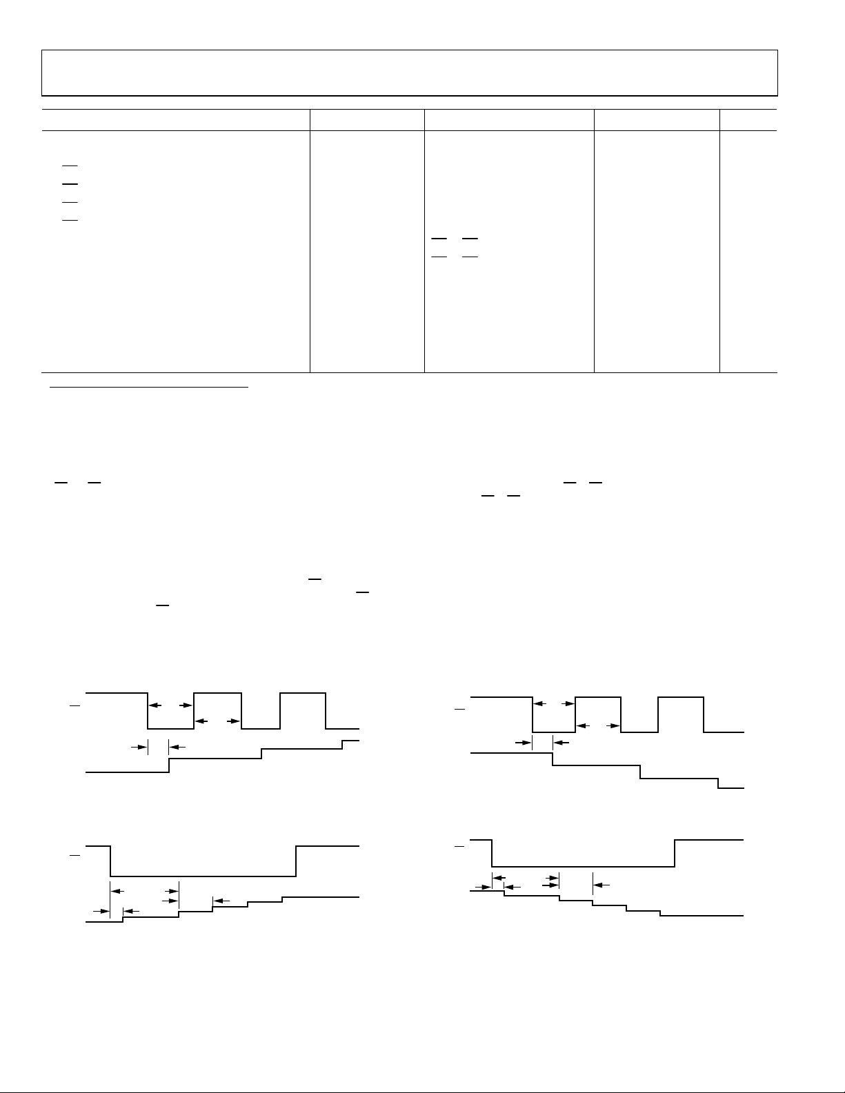
INTERFACE TIMING DIAGRAMS
t
PU
R
WB
PU
R
WB
PU
t
PU_REP
t
DB
Figure 2. Increment R
t
AS_START
t
DB
t
AS
Figure 3. Increment R
in Discrete Steps
WB
in Autoscan Mode
WB
04422-0-004
04422-0-005
Rev. 0 | Page 4 of 20
t
PU
R
WB
PD
t
PD_REP
t
DB
Figure 4. Decrement R
in Discrete Steps
WB
04422-0-006
PD
t
AS_START
t
R
WB
DB
Figure 5. Decrement R
t
AS
04422-0-007
in Autoscan Mode
WB
Page 5

AD5228
ABSOLUTE MAXIMUM RATINGS
Table 3.
Parameter Rating
VDD to GND −0.3 V, +7 V
VA, VB, VW to GND 0 V, VDD
0 V, V
PU, PD, PRE Voltage to GND
DD
Maximum Current
IWB, IWA Pulsed ±20 mA
IWB Continuous (R
≤ 5 kΩ, A open)1 ±1 mA
WB
IWA Continuous (RWA ≤ 5 kΩ, B open)1 ±1 mA
IAB Continuous
= 10 kΩ/50 kΩ/100 kΩ)1
(R
AB
±500 µA/±100 µA/
±50 µA
Operating Temperature Range −40°C to +105°C
Maximum Junction Temperature
(T
max)
J
150°C
Storage Temperature −65°C to +150°C
Lead Temperature
245°C
(Soldering, 10 s – 30 s)
Thermal Resistance2 θJA 230°C/W
1
Maximum terminal current is bounded by the maximum applied voltage
across any two of the A, B, and W terminals at a given resistance, the
maximum current handling of the switches, and the maximum power
dissipation of the package. VDD = 5 V.
2
Package power dissipation = (TJmax – TA) / θJA.
Stresses above those listed under Absolute Maximum Ratings
may cause permanent damage to the device. This is a stress
rating only and functional operation of the device at these or
any other conditions above those indicated in the operational
section of this specification is not implied. Exposure to absolute
maximum rating conditions for extended periods may affect
device reliability.
ESD CAUTION
ESD (electrostatic discharge) sensitive device. Electrostatic charges as high as 4000 V readily accumulate on
the human body and test equipment and can discharge without detection. Although this product features
proprietary ESD protection circuitry, permanent damage may occur on devices subjected to high energy
electrostatic discharges. Therefore, proper ESD precautions are recommended to avoid performance
degradation or loss of functionality.
Rev. 0 | Page 5 of 20
Page 6

AD5228
PIN CONFIGURATION AND FUNCTION DESCRIPTIONS
PU
1
PD
2
A
3
4
GND
Figure 6. SOT-23-8 Pin Configuration
Table 4. Pin Function Descriptions
Pin No. Mnemonic Description
1
Push-Up Pin.
PU
Connect to the external pushbutton. Active low. A 100 kΩ pull-up resistor is connected to V
2
Push-Down Pin.
PD
Connect to the external pushbutton. Active low. A 100 kΩ pull-up resistor is connected to V
3 A Resistor Terminal A. GND ≤VA ≤ VDD.
4 GND Common Ground.
5 W Wiper Terminal W. GND ≤ VW ≤ VDD.
6 B Resistor Terminal B. GND ≤ VB ≤ VDD.
7 PRE
Power-On Preset. Output = midscale if PRE = GND; output = zero scale if PRE = V
No pull-up resistor is needed.
8 VDD Positive Power Supply, 2.7 V to 5.5 V.
AD5228
V
8
DD
PRE
7
B
6
5
W
04422-0-003
.
DD
.
DD
. Do not let the PRE pin float.
DD
Rev. 0 | Page 6 of 20
Page 7

AD5228
TYPICAL PERFORMANCE CHARACTERISTICS
0.10
0.08
0.06
0.04
0.02
0
–0.02
–0.04
RHEOSTAT MODE INL (LSB)
–0.06
–0.08
–0.10
032282420161284
CODE (Decimal)
Figure 7. R-INL vs. Code vs. Supply Voltages
0.10
0.08
0.06
0.04
0.02
0
–0.02
–0.04
RHEOSTAT MODE INL (LSB)
–0.06
–0.08
–0.10
032282420161284
CODE (Decimal)
Figure 8. R-INL vs. Code vs. Temperature, V
0.10
0.08
0.06
–0.02
–0.04
RHEOSTAT MODE DNL (LSB)
–0.06
–0.08
–0.10
0.04
0.02
0
032282420161284
2.7V
CODE (Decimal)
Figure 9. R-DNL vs. Code vs. Supply Voltages
2.7V
5.5V
5.5V
TA = 25°C
–40°C
+25°C
+85°C
+105°C
VDD = 5.5V
= 5 V
DD
TA = 25°C
04422-0-008
04422-0-009
04422-0-010
0.10
0.08
0.06
0.04
0.02
0
–0.02
–0.04
RHEOSTAT MODE DNL (LSB)
–0.06
–0.08
–0.10
032282420161284
CODE (Decimal)
Figure 10. R-DNL vs. Code vs. Temperature, V
0.10
0.08
0.06
0.04
–0.02
–0.04
–0.06
POTENTIOMETER MODE INL (LSB)
–0.08
–0.10
0.02
0
5.5V
032282420161284
CODE (Decimal)
Figure 11. INL vs. Code vs. Supply Voltages
0.10
0.08
0.06
0.04
0.02
0
–0.02
–0.04
–0.06
POTENTIOMETER MODE INL (LSB)
–0.08
–0.10
032282420161284
CODE (Decimal)
Figure 12. INL vs. Code, V
DD
= 5 V
–40°C
+25°C
+85°C
+105°C
VDD = 5.5V
= 5 V
DD
TA = 25°C
2.7V
–40°C
+25°C
+85°C
+105°C
VDD = 5.5V
04422-0-011
04422-0-012
04422-0-013
Rev. 0 | Page 7 of 20
Page 8

AD5228
–
0.10
0.08
0.06
–0.02
–0.04
–0.06
POTENTIOMETER MODE DNL (LSB)
–0.08
–0.10
–0.02
–0.04
–0.06
POTENTIOMETER MODE DNL (LSB)
–0.08
–0.10
–0.55
–0.60
–0.65
–0.70
FSE (LSB)
–0.75
–0.80
–0.85
–0.90
0.04
0.02
0
0.10
0.08
0.06
0.04
0.02
0
0.50
5.5V
032282420161284
CODE (Decimal)
Figure 13. DNL vs. Code vs. Supply Voltages
032282420161284
CODE (Decimal)
Figure 14. DNL vs. Code, V
VDD = 5.5V
= 2.7V
V
DD
–40 –20 0 20 40 60 10080
TEMPERATURE (°C)
Figure 15. Full-Scale Error vs. Temperature
DD
= 5 V
TA = 25°C
–40°C
+25°C
+85°C
+105°C
VDD = 5.5V
2.7V
04422-0-014
04422-0-015
04422-0-016
0.50
0.45
0.40
= 2.7V
0.35
0.30
0.25
ZSE (LSB)
0.20
0.15
0.10
0.05
0
–40 –20 0 20 40 60 10080
V
DD
VDD = 5.5V
TEMPERATURE (°C)
Figure 16. Zero-Scale Error vs. Temperature
1
A)
µ
SUPPLY STANDBY CURRENT (
0.1
–40 –20 0 20 40 60 10080
TEMPERATURE (°C)
Figure 17. Supply Current vs. Temperature
120
100
(kΩ)
AB
80
60
40
NOMINAL RESISTANCE R
20
0
–40 –20 0 20 40 60 10080
RAB = 100kΩ
R
= 50kΩ
AB
R
= 10kΩ
AB
TEMPERATURE (°C)
Figure 18. Nominal Resistance vs. Temperature
VDD = 5.5V
I
DD_ACT
VDD = 5.5V
04422-0-017
= 50µA TYP
04422-0-018
04422-0-019
Rev. 0 | Page 8 of 20
Page 9

AD5228
/DIV
R
z
/DIV
R
z
/DIV
R
z
120
VDD = 2.7V
100
(Ω)
W
80
60
V
= 5.5V
DD
40
WIPER RESISTANCE, R
20
0
–40 –20 0 20 40 60 10080
TEMPERATURE (°C)
Figure 19. Wiper Resistance vs. Temperature
150
120
T (ppm/°C)
∆
/
WB
90
R
∆
60
30
0
RHEOSTAT MODE TEMPCO,
–30
0 4 8 121620242832
CODE (Decimal)
Figure 20. Rheostat Mode Tempco ∆R
/∆T vs. Code
WB
20
C)
°
15
T (ppm/
∆
/
10
WB
V
∆
5
0
–5
–10
–15
POTENTIOMETER MODE TEMPCO,
–20
0 4 8 12 16 20 24 28 32
CODE (Decimal)
VDD = VA = 5.5V
= 0V
V
B
10kΩ
50kΩ
100kΩ
VDD = 5.5V
A = OPEN
10kΩ
50kΩ
100kΩ
04422-0-020
04422-0-021
04422-0-022
REF LEVEL
0dB
6
6.0dB
0
–6
–12
–18
–24
GAIN (dB)
–30
16 STEPS
8 STEPS
4 STEPS
2 STEPS
1 STEP
MARKE
MAG (A/R)
TA = 25°C
V
DD
= 50mV rms
V
A
–36
–42
–48
–54
1k 10k 1M
START 1 000.000Hz STOP 1 000 000.000Hz
Figure 22. Gain vs. Frequency vs. Code, R
100k
= 10 kΩ
AB
REF LEVEL
0dB
6
6.0dB
0
–6
–12
–18
–24
GAIN (dB)
–30
16 STEPS
8 STEPS
4 STEPS
2 STEPS
1 STEP
–36
–42
–48
–54
1k 10k 1M
START 1 000.000Hz STOP 1 000 000.000Hz
Figure 23. Gain vs. Frequency vs. Code, R
MARKE
MAG (A/R)
100k
TA = 25°C
V
DD
= 50mV rms
V
A
= 50 kΩ
AB
REF LEVEL
0dB
6
6.0dB
0
–6
–12
–18
–24
GAIN (dB)
–30
16 STEPS
8 STEPS
4 STEPS
2 STEPS
1 STEP
–36
–42
–48
–54
1k 10k 1M
START 1 000.000Hz STOP 1 000 000.000Hz
MARKE
MAG (A/R)
100k
TA = 25°C
V
DD
= 50mV rms
V
A
469 390.941H
–8.966dB
= 5.5V
97 525.233H
–9.089dB
= 5.5V
51 404.427H
–9.123dB
= 5.5V
04422-0-050
04422-0-051
04422-0-052
Figure 21. Potentiometer Mode Tempco ∆V
/∆T vs. Code
WB
Figure 24. Gain vs. Frequency vs. Code, R
= 100 kΩ
AB
Rev. 0 | Page 9 of 20
Page 10

AD5228
0
–20
STEP = MIDSCALE, VA = VDD, VB = 0V
PU
1
VDD= 5V DC±10% p-p AC
PSRR (dB)
VDD= 3V DC±10% p-p AC
–40
–60
100 1k 10k 100k 1M
FREQUENCY (Hz)
Figure 25. PSRR
∆: 8.32ms ∆: 4.00mV
@: 8.24ms @: 378mV
1
VDD = 5V
= 5V
V
A
= 0V
V
B
2
CH1 5.00V CH2 100mV M2.00ms A CH1 3.00V
T 3.92000ms
Figure 26. Basic Increment
PU
V
W
04422-0-027
04422-0-026
VDD = 5V
V
A
V
2
CH1 5.00V CH2 200mV M2.00ms A CH1 2.80V
T 800.000ms
B
Figure 28. Autoscan Increment
1.2
1.0
(mA)
0.8
WB_MAX
0.6
0.4
THEORETICAL I
0.2
0
032282420161284
RAB = 50k
RAB = 100k
Ω
Figure 29. Maximum I
Ω
CODE (Decimal)
RAB = 10k
vs. Code
WB
= 5V
= 0V
VA = OPEN
T
= 25°C
A
Ω
V
W
04422-0-029
04422-0-030
1
VDD = 5V
= 5V
V
2
CH1 5.00V CH2 100mV M2.00ms A CH1 2.60V
T 59.8000ms
A
= 0V
V
B
Figure 27. Repetitive Increment
PU
V
W
04422-0-028
Rev. 0 | Page 10 of 20
Page 11

AD5228
THEORY OF OPERATION
The AD5228 is a 32-position manual up/down digitally controlled potentiometer with selectable power-on preset. The
AD5228 presets to midscale when the PRE pin is tied to ground
and to zero-scale when PRE is tied to V
is not allowed. The step-up and step-down operations require
the activation of the
(push-up) and PD (push-down) pins.
PU
These pins have 100 kΩ internal pull-up resistors that the
and
activate at logic low. The common practice is to apply
PD
external pushbuttons (tactile switches) as shown in Figure 30.
UP/DOWN
CONTROL
LOGIC
DISCRETE
STEP/AUTO
SCAN DETECT
ADAPTIVE
DEBOUNCER
PUSH-UP
BUTTON
PUSH-DOWN
BUTTON
V
DD
R1 R2
PU
PD
Figure 30. Typical Pushbutton Interface
. Floating the PRE pin
DD
D
AD5228
E
C
O
D
E
ZERO- OR MID-
SCALE PRESET
PRE GND
PU
A
W
B
04422-0-031
1
CH1 1.00V M100µs A CH1 2.38V
T 20.20%
Figure 32. Close-Up of Initial Bounces
04422-0-033
Because of the bounce mechanism commonly found in the
switches during contact closures, a single pushbutton press
usually generates numerous bounces during contact closure.
Note that the term pushbutton refers specifically to a
pushbutton tactile switch or a similar switch that has 10 ms or
less bounce time during contact closure. Figure 31 shows the
characteristics of one such switch, the KRS-3550 tactile switch.
Figure 32 and Figure 33 show close ups of the initial bounces
and end bounces, respectively.
1
CH1 1.00V M40.0ms A CH1 2.38V
T 20.40%
Figure 31. Typical Tactile Switch Characteristics
04422-0-032
1
CH1 1.00V M10.0µs A CH1 2.38V
T 20.20%
04422-0-034
Figure 33. Close-Up of Final Bounces
The following paragraphs describes the PU incrementing
operation. Similar characteristics apply to the
decrementing
PD
operation.
The AD5228 features an adaptive debouncer that monitors the
duration of the logic-low level of
logic-low level signal duration is shorter than 7 ms, the
the
PU
signal between bounces. If
PU
debouncer ignores it as an invalid incrementing command.
Whenever the logic-low level of
signal lasts longer than
PU
11 ms, the debouncer assumes that the last bounce is met and
therefore increments R
Repeatedly pressing the
by one step.
WB
button for fast adjustment without
PU
missing steps is allowed, provided that each press is not shorter
, which is 12 ms (see Figure 2). As a point of reference,
than t
PU
an advanced video game player can press a pushbutton switch
in 40 ms.
Rev. 0 | Page 11 of 20
Page 12

AD5228
(
(
If the PU button is held for longer than 1 second, continuously
holding it activates autoscan mode such that the AD5228
increments by four R
Whenever the maximum R
incrementing regardless of the state of the
ous holding of the
current.
When both
and PD buttons are pressed, RWB decrements
PU
until it stops at zero scale.
All the preceding descriptions apply to
the tolerance of the internal RC oscillator, all the timing
information given previously is based on the typical values,
which can vary ±30%.
The AD5228 debouncer is carefully designed to handle common
pushbutton tactile switches. Other switches that have excessive
bounces and duration are not suitable to use in conjunction
with the AD5228.
Figure 34. AD5228 Equivalent RDAC Circuit
PROGRAMMING THE DIGITAL POTENTIOMETERS
Rheostat Operation
If only the W-to-B or W-to-A terminals are used as variable
resistors, the unused terminal can be opened or shorted with W.
Such operation is called rheostat mode and is shown in Figure 35.
Figure 35. Rheostat Mode Configuration
steps per second (see Figure 3).
WB
(= RAB) is reached, RWB stops
WB
pin. Any continu-
PU
pin to logic-low simply elevates the supply
PU
operation. Due to
PD
A
R
S
D0
R
D1
D2
D3
D4
RDAC
UP/DOWN
CTRL AND
DECODE
A
B
S
R
S
W
R
W
R
S
R
=
RAB/32
S
A
W
W
B
B
04422-0-035
A
W
B
04422-0-036
The end-to-end resistance, RAB, has 32 contact points accessed
by the wiper terminal, plus the B terminal contact if R
Pushing the
total resistance becomes R
change of R
pin discretely increments RWB by one step. The
PU
+ RW as shown in Figure 34. The
S
can be determined by the number of discrete PU
WB
is used.
WB
executions provided that its maximum setting is not reached
during operation. ∆R
WB
WB
can, therefore, be approximated as
WB
R
⎛
AB
PUR
⎜
32
⎝
R
⎛
AB
PDR
⎜
32
⎝
⎞
++=∆
R
(1)
⎟
W
⎠
⎞
+−=∆
R
(2)
⎟
W
⎠
where:
is the number of push-up executions.
PU
is the number of push-down executions.
PD
is the end-to-end resistance.
R
AB
is the wiper resistance contributed by the on-resistance of
R
W
the internal switch.
Similar to the mechanical potentiometer, the resistance of the
RDAC between the Wiper W and Terminal A also produces a
complementary resistance, R
the B terminal can be opened or shorted to W. R
. When these terminals are used,
WA
can also be
WA
approximated if its maximum and minimum settings are not
reached.
WA
WA
⎛
32
⎜
⎝
⎛
32
⎜
⎝
R
AB
)
PUR
32
R
AB
)
PDR
32
Note that Equations 1 to 4 do not apply when
⎞
R
+−−=∆
3)
⎟
W
⎠
⎞
R
+−+=∆
(4)
⎟
W
⎠
and PD = 0
PU
execution.
Because in the lowest end of the resistor string, a finite wiper
resistance is present, care should be taken to limit the current
flow between W and B in this state to a maximum pulse current
of no more than 20 mA. Otherwise, degradation or possible
destruction of the internal switches can occur.
The typical distribution of the resistance tolerance from device
to device is process lot dependent, and ±20% tolerance is possible.
Rev. 0 | Page 12 of 20
Page 13

AD5228
Potentiometer Mode Operation
If all three terminals are used, the operation is called potentiometer mode. The most common configuration is the voltage
divider operation as shown in Figure 36.
V
I
A
V
C
W
B
04422-0-037
Figure 36. Potentiometer Mode Configuration
The change of VWB is known provided that the AD5228
maximum or minimum scale has not been reached during
operation. If the effect of wiper resistance is ignored, the
transfer functions can be simplified as
PU
V
V
V
+=∆ (5)
AWB
32
PD
V
+=∆ (6)
AWB
32
Unlike in rheostat mode operation where the absolute tolerance
is high, potentiometer mode operation yields an almost ratiometric function of
contributed by the R
almost canceled. Although the thin film step resistor R
CMOS switch resistance, R
/32 or PD/32 with a relatively small error
PU
term. The tolerance effect is, therefore,
W
S
, have very different temperature
W
and
coefficients, the ratiometric adjustment also reduces the overall
temperature coefficient effect to 5 ppm/°C except at low value
codes where R
dominates.
W
Potentiometer mode operations include an op amp input and
feedback resistors network and other voltage scaling applications.
The A, W, and B terminals can be input or output terminals and
have no polarity constraint provided that |V
do not exceed V
-to-GND.
DD
|, |VWA|, and |VWB|
AB
CONTROLLING INPUTS
All PU and PD inputs are protected with a Zener ESD structure
as shown in Figure 37.
V
DD
100kΩ
PU
Figure 37. Equivalent ESD Protection in
and PD pins are usually connected to pushbutton tactile
PU
DECODE
AND
DEBOUNCE
CKT
04422-0-038
PU
and PD Pins
switches for manual operation, but the AD5228 can also be
controlled digitally. It is recommended to add external
MOSFETs or transistors that simplify the logic controls.
D
AD5228
E
C
O
D
E
ZERO- OR MID-
SCALE PRESET
PRE GND
A
W
B
UP
2N7002
UP/DOWN
V
DD
R1 R2
PU
N1
PD
N2
DOWN
2N7002
CONTROL
LOGIC
DISCRETE
STEP/AUTO
SCAN DETECT
ADAPTIVE
DEBOUNCER
Figure 38. Digital Control with External MOSFETs
TERMINAL VOLTAGE OPERATION RANGE
The AD5228 is designed with internal ESD diodes for
protection. These diodes also set the voltage boundary of the
terminal operating voltages. Positive signals present on
Ter mi n al A, B , o r W t h at e xc e ed V
forward-biased diode. There is no polarity constraint between
, VW, and VB, but they cannot be higher than VDD or lower
V
A
than GND.
are clamped by the
DD
V
DD
04422-0-039
Rev. 0 | Page 13 of 20
A
W
B
GND
4422-0-040
Figure 39. Maximum Terminal Voltages Set by V
and GND
DD
Page 14

AD5228
POWER-UP AND POWER-DOWN SEQUENCES
Because of the ESD protection diodes that limit the voltage
compliance at Terminals A, B, and W (Figure 39), it is important
to power on V
and W. Otherwise, the diodes are forward-biased such that V
is powered on unintentionally and can affect other parts of the
circuit. Similarly, V
power-on sequence is in the following order: GND, V
. The order of powering VA, VB, and VW is not important
V
A/B/W
as long as they are powered on after V
and
pins can be logic high or floating, but they should not
PD
be logic low during power-on.
before applying any voltage to Terminals A, B,
DD
should be powered down last. The ideal
DD
, and
DD
. The states of the PU
DD
DD
LAYOUT AND POWER SUPPLY BIASING
It is always a good practice to use compact, minimum lead
length layout design. The leads to the input should be as direct
as possible with a minimum conductor length. Ground paths
should have low resistance and low inductance. It is also good
practice to bypass the power supplies with quality capacitors.
Low ESR (equivalent series resistance) 1 µF to 10 µF tantalum
or electrolytic capacitors should be applied at the supplies to
minimize any transient disturbance and to filter low frequency
ripple. Figure 39 illustrates the basic supply bypassing configuration for the AD5228.
AD5228
V
DD
+
C2
10µFC10.1µF
Figure 40. Power Supply Bypassing
V
DD
GND
04422-0-041
Rev. 0 | Page 14 of 20
Page 15

AD5228
APPLICATIONS
MANUAL ADJUSTABLE LED DRIVER
The AD5228 can be used in many electronics-level adjustments
such as LED drivers for LCD panel backlight controls. Figure 41
shows a manually adjustable LED driver. The AD5228 sets the
voltage across the white LED D1 for the brightness control.
Since U2 handles up to 250 mA, a typical white LED with V
F
of
3.5 V requires a resistor, R1, to limit U2 current. This circuit is
simple but not power efficient. The U2 shutdown pin can be
toggled with a PWM signal to conserve power.
5V
C1
1µFC20.1µF
PUSH-UP
BUTTON
PUSH-DOWN
BUTTON
V
PU
PD
U1
AD5228
DD
A
W
10kΩ
B
GNDPRE
Figure 41. Low Cost Adjustable LED Driver
5V
V+
–
U2
AD8591
+
V–
C3
0.1µF
PWM
R1
SD
6Ω
WHITE
LED
D1
04422-0-042
ADJUSTABLE CURRENT SOURCE FOR LED DRIVER
Because LED brightness is a function of current rather than of
forward voltage, an adjustable current source is preferred as
shown in Figure 42. The load current can be found as the V
the AD5228 divided by R
V
WB
I =
D1
(7)
R
SET
SET
.
The U1 ADP3333ARM-1.5 is a 1.5 V LDO that is lifted above or
lowered below 0 V. When VWB of the AD5228 is at its minimum,
there is no current through D1, so the GND pin of U1 is at –1.5 V
if U3 is biased with the dual supplies. As a result, some of the U2
low resistance steps have no effect on the output until the U1
GND pin is lifted above 0 V. When V
maximum, V
becomes VL + VAB, so the U1 supply voltage
OUT
of the AD5228 is at its
WB
must be biased with adequate headroom. Similarly, PWM signal
can be applied at the U1 shutdown pin for power efficiency.
V
5V
INVOUT
U1
ADP3333
ARM-1.5
PWM
SD
GND
5V
PUSH-UP
BUTTON
PUSH-DOWN
BUTTON
V
PRE
PU
PD
DD
Figure 42. Adjustable Current Source for LED Driver
GND
U2
AD5228
B
W
10kΩ
A
R1
418kΩ
5V
V+
U3
AD8591
V–
R
SET
0.1Ω
–
+
VL
D1
of
WB
ID
04422-0-043
ADJUSTABLE HIGH POWER LED DRIVER
The previous circuit works well for a single LED. Figure 43
shows a circuit that can drive three to four high power LEDs.
The ADP1610 is an adjustable boost regulator that provides the
voltage headroom and current for the LEDs. The AD5228 and
the op amp form an average gain of 12 feedback network that
servos the R
reference voltage. As the loop is set, the voltage across R
regulated around 0.1 V and adjusted by the digital
potentiometer.
I
LED
should be small enough to conserve power but large enough
R
SET
to limit maximum LED current. R3 should also be used in parallel with AD5228 to limit the LED current within an achievable
range. A wider current adjustment range is possible by lowering
the R2 to R1 ratio as well as changing R3 accordingly.
5V
C2
10µF
L1–SLF6025-100M1R0
D1–MBR0520LT1
voltage and the ADP1610 FB pin 1.2 V band gap
SET
is
SET
V
R
SET
(8)
=
R
SET
13.5kΩ
R4
PWM
1.2V
R
C
100kΩ
C
C
390pF
C8
0.1µF
U1
R2
1.1kΩ
IN
U2
ADP1610
SD
FB
COMP
SS RT GND
V+
C
SS
10nF
5V
SW
U3
+
AD8541
–
V–
L1
10µF
D1
U1
AD5228
W
BA
10kΩ
R3
200Ω
C3
10µF
R
0.25Ω
R1
100Ω
SET
V
OUT
D2
D3
D4
Figure 43. Adjustable Current Source for LEDs in Series
04422-0-044
Rev. 0 | Page 15 of 20
Page 16

AD5228
±
AUTOMATIC LCD PANEL BACKLIGHT CONTROL
With the addition of a photocell sensor, an automatic brightness
control can be achieved. As shown in Figure 44, the resistance of
the photocell changes linearly but inversely with the light
output. The brighter the light output, the lower the photocell
resistance and vice versa. The AD5228 sets the voltage level that
is gained up by U2 to drive N1 to a desirable brightness. With
the photocell acting as the variable feedback resistor, the change
in the light output changes the R2 resistance, therefore causing
U2 to drive N1 accordingly to regulate the output. This simple
low cost implementation of an LED controller can compensate
for the temperature and aging effects typically found in high
power LEDs. Similarly, for power efficiency, a PWM signal can
be applied at the gate of N2 to switch the LED on and off
without noticeable effect.
C1
1µFC20.1µF
PUSH-UP
BUTTON
PUSH-DOWN
BUTTON
5V
R2
R1
PHOTOCELL
1kΩ
PU
PD
5V
U1
AD5228
V
DD
A
W
10kΩ
B
GNDPRE
5V
V+
–
U2
AD8531
+
V–
C3
0.1µF
PWM
R3
4.75kΩ
N2
Figure 44. Automatic LCD Panel Backlight Control
N1
2N7002
5V
WHITE
LED
D1
2N7002
AUDIO AMPLIFIER WITH VOLUME CONTROL
The AD5228 and SSM2211 can form a 1.5 W audio amplifier
with volume control that has adequate power and quality for
portable devices such as PDAs and cell phones. The SSM2211
can drive a single speaker differentially between Pins 5 and 8
without any output capacitor. The high-pass cutoff frequency is
= 1/(2 × π × R1 × C1). The SSM2211 can also drive two
f
H1
speakers as shown in Figure 45. However, the speakers must be
configured in single-ended mode, and output coupling capacitors
are needed to block the dc current. The output capacitor and
the speaker load form an additional high-pass cutoff frequency
= 1/(2 × π × R5 × C3). As a result, C3 and C4 must be
as f
H2
large to make the frequency as low as f
AUDIO_INPUT
5V
C6
10µFC70.1µF
PUSH-UP
BUTTON
PUSH-DOWN
BUTTON
5V
R3
10kΩ
R4
10kΩ
04422-0-045
2.5V p-p
U1
V
DD
PRE
A
1µF
W
10kΩ
B
GND
–
U3
AD8591
+
PU
PD
Figure 45. Audio Amplifier with Volume Control
.
H1
R2
10kΩ
C5
5V
0.1µF
C1
R1
10kΩ
4
–
V+
U2
SSM2211
3
V–
+
7
2
C2
0.1µF
C3
470µF
6
1
5
8
C44
470µF
R5
8Ω
R6
8Ω
04422-0-046
Rev. 0 | Page 16 of 20
Page 17

AD5228
V
CONSTANT BIAS WITH SUPPLY TO RETAIN RESISTANCE SETTING
Users who consider EEMEM potentiometers but cannot justify
the additional cost and programming for their designs can
consider constantly biasing the AD5228 with the supply to
retain the resistance setting as shown in Figure 46. The AD5228
is designed specifically with low power to allow power conservation even in battery-operated systems. As shown in Figure 47,
a similar low power digital potentiometer is biased with a 3.4 V
450 mA/hour Li-Ion cell phone battery. The measurement shows
that the device drains negligible power. Constantly biasing the
potentiometer is a practical approach because most of the
portable devices do not require detachable batteries for charging.
Although the resistance setting of the AD5228 is lost when the
battery needs to be replaced, this event occurs so infrequently
that the inconvenience is minimal for most applications.
DD
SW1
U1
AD5228
V
DD
+
U2
V
DD
COMPONENT X
U3
V
DD
COMPONENT Y
3.50
3.49
3.48
3.47
3.46
3.45
3.44
3.43
BATTERY VOLTAGE (V)
3.42
3.41
3.40
024681012
DAYS
TA = 25°C
Figure 47. Battery Consumption Measurement
04422-0-048
BATTERY OR
GND
SYSTEM POWER
–
GND
GND
GND
04422-0-047
Figure 46. Constant Bias AD5228 for Resistance Retention
Rev. 0 | Page 17 of 20
Page 18

AD5228
OUTLINE DIMENSIONS
2.90 BSC
847
1.60 BSC
PIN 1
0.90
0.87
0.84
0.10 MAX
1 3562
1.95
BSC
0.38
0.22
COMPLIANT TO JEDEC STANDARDS MO-193BA
2.80 BSC
0.65 BSC
1.00MAX 0.20
SEATING
PLANE
0.08
8°
4°
0°
0.60
0.45
0.30
Figure 48. 8-Lead Small Outline Transistor Package TSOT-8 [Thin SOT-23-8]
(UJ-8)
Dimensions shown in millimeters
ORDERING GUIDE
Full Container
Model1 RAB (kΩ) Temperature Range Package Code Package Description
AD5228BUJZ102-RL7 10 −40°C to +105°C UJ TSOT-8 3000 D3K
AD5228BUJZ102-R2 10 −40°C to +105°C UJ TSOT-8 250 D3K
AD5228BUJZ502-RL7 50 −40°C to +105°C UJ TSOT-8 3000 D3L
AD5228BUJZ502-R2 50 −40°C to +105°C UJ TSOT-8 250 D3L
AD5228BUJZ1002-RL7 100 −40°C to +105°C UJ TSOT-8 3000 D3M
AD5228BUJZ1002-R2 100 −40°C to +105°C UJ TSOT-8 250 D3M
AD5228EVAL 10 Evaluation Board 1
1
The end-to-end resistance R
example,10 kΩ = 10.
2
Z = Pb-free part.
is available in 10 kΩ, 50 kΩ, and 100 kΩ. The final three characters of the part number determine the nominal resistance value, for
AB
Quantity
Branding
Rev. 0 | Page 18 of 20
Page 19

AD5228
NOTES
Rev. 0 | Page 19 of 20
Page 20

AD5228
NOTES
© 2004 Analog Devices, Inc. All rights reserved. Trademarks and
registered trademarks are the property of their respective owners.
D04422–0–4/04(0)
Rev. 0 | Page 20 of 20
 Loading...