

Page 1
ANALOGDEVICES fAX-ON-DEHAND HOTLINE
查询AD509供应商查询AD509供应商
- Page 12
.'
r. ANALOG
LIllI
DEVICES
FastSettlingIe UpAmp
HighSpeed,
. AD509 I
FEATURES
Fat Settting Time
~O.1'" in 5OOns mex
0.01% in 2.5ps max
High Slew Rate: 100V/1lS min'
Low 10': 25nA max
Guaranteed VOl Drift: 3OIlVrC mex
High CMRR: BOdBmin
Orive.5OOpF
Low Price
APPLICATIONS
01A and AID Converlion
Wideband Amplifi8n
MultiplexeR
Pul. AmplifieR
INVERTINGr2
OBSOLETE
PRODUCT DESCRIPTION
The ADS09j, ADS09K and ADS09S are monolithic
operational amplifiers specifically designed for applications
requiring fast settling times to high accuracy. Other compar-
able dynamic parameters include a small signal bandwidth of
2OMHz, slew rate of lOOV/JlS min and a full power response
of 150kHz min. The devices are internally compensated for
all closed loop gains greater than 3, and are compensated with
a single capacitor for lower gains.
The input characteristics of the AD.509 are consistent with
0.01 % accuracy over limited temperature ranges; offset current
is 2SnA max, offset voltage is 8mV max, nullable to' zero, and
offset voltage drift is limited to 30p.V/'C max. PSRR and
CMRR are typically 90dB.
The ADS09 is designed for use with high speed D/A or AID
conveners where the minimum conversion time is limited by
the amplifier setding time. If 0.01 % accuracy of conversion
is required. a conversion cannot be made in a shoner period
than the time required for the amplifier to settle to within
0.01 % of its final value,
All devices are supplied in the TO-99 package. The ADS09j
and ADS09K are specified for 0 to +70oC temperatUte range;
the ADS09S for operation from -SSoC to +12SoC.
PRODUCT HIGHLIGHTS
1. The ADS09 is internally compensated for all closed loop
gains above 3. and compensated with a single capacitor for
lower gains thus eliminating the c:laborate stabilizing tech-
niques required by other high speed IC op amps.
2. The ADSO9 will drive capaciti~ loads of SOOpF without
deterioration in settling time. Larger capacitive loads
can be driven by tailoring the compensation to minimize
settling time.
3. Common Mode Rejection, Gain and Noise are compatible
with a 0.01% accuracy device.
4. The ADSO9K and ADSO9S are 100% tested for minimum
slew rate and guaranteed to settle to 0.01% of its final
value in less than 2.Slls.
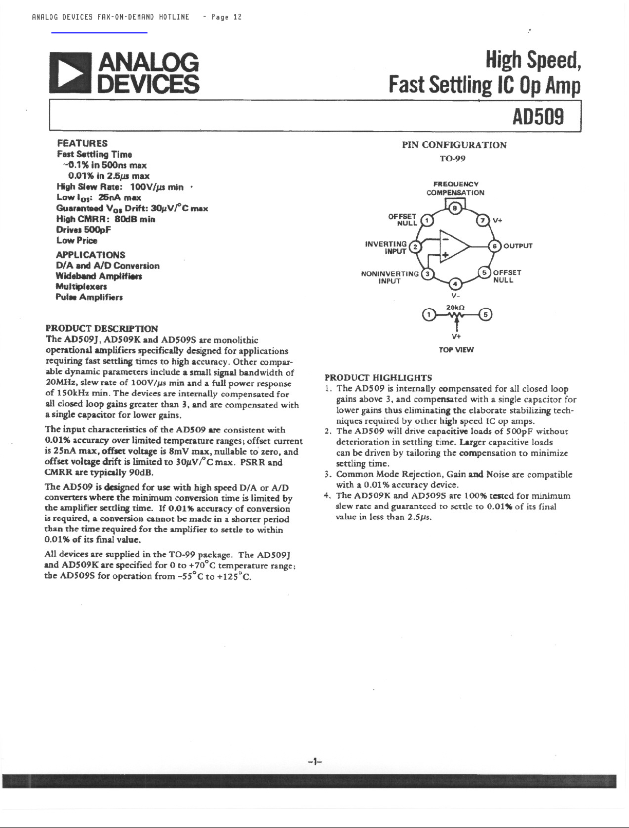
PIN CONFIGURATION
TO-99
FREQUENCY
COMPENSATION
INPUT
~
2.. T !.
TOPVIEW
v-
V+
-1-
Page 2
ANALOGDEVICES fAX-ON-DEMAND HOTLINE
- Page 13
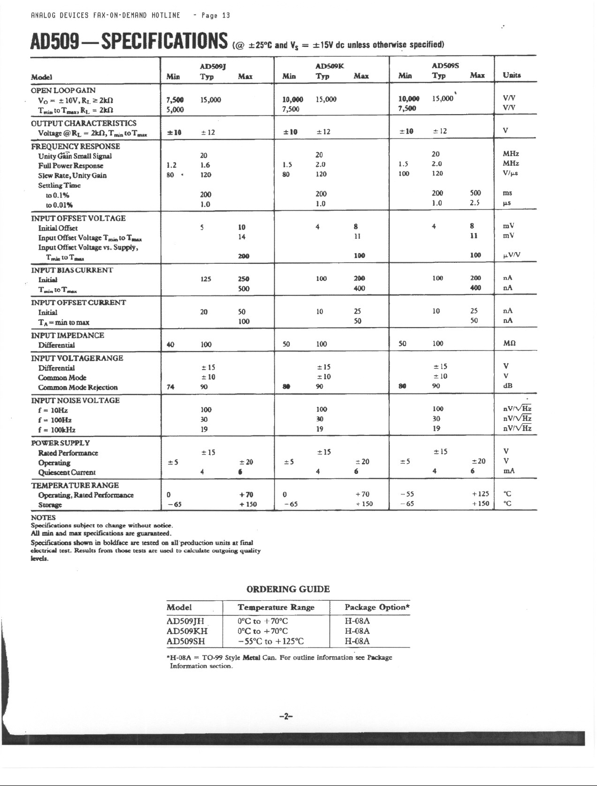
AD509-SPECIFICATIONS(@ %25°&andVs= %15Vdeunlessoth8lWi~e specified)
,.
Model
OPEN LOOP GAIN
Vo = :t10V,RL2:2kO
TmiDtoT...,RL '" 2kO
OUTPUT CHARACTERISTICS
Voltage@RL = 2k.O,T....D[oT-
FREQUENCY RESPONSE
Unity<din Small Sipal
Full Power Response
SlewRate, UnityGain
SettlingTime
100.1%
100.01%
INPUT OFFSET VOLTAGE
InitialOffset
Input Offset Voltage TmiDto T...
Input Off8CIVoltageVI.Supply,
T.....toT...
INPUT BIASCURRENT
l'Di0ai
T...toT-
OBSOLETE
INPUT OFFSET CURRENT
Initial
T,,=minlOmax
INPUT IMPEDANCE
Differential
INPUT VOLTAGE RANGE
Differential
CommooMode
CommonModeRejection
INPUT NOISE VOLTAGE
f = 10Hz
f'" 100Hz
f=]OOIt}h
POWER SUPPLY
Rated Perfonnana:
Opcnting
QuicsceD[Current
TEMPERATURE RANGE
Opcnting. Rated Performanc:e
SIOtllF
NOTES
SpecifICationS subject to cbanae without DOrice,
AU miA and mu specuJCations are guarm>teed,
SpecifJCaDoaSshown ill boldface are tared on all 'prodUCtion units at fmal
dectric:aI tat. Results from t~ tests are used to calculate outgoing quality
Ie¥$.
MiD
7,500 15,000
5,000
:10 :t 12
1.2 J.6
80' 120
4()
74
:5
0 +70
-65 +150 -65
AD5O9J
Typ
20
200
1.0
5
125 250
20
100
: 15 : 15
: 10
90
100
30
19
:!:]5 ::!:15
4 '
Mas MiD
10,000 15,000
7,500
:10
l.5 2,0
80 120
10
14
2OCt
SOO
50 10
100
50 100 50 100
at 90
:20 ::5 :!:20 :!:5
0 +70
AD5O9K
Typ
:!:12
20
200
1.0 1.0
4
100
,dO
100
30
19
Max MiD
10,000
7,500
:tICI :!:12
1.5
100
8 4 8
11 11
100
200 100
400
25 10 25
50 50
80 90 dB
4 6
-55
+ 150 -65
AD509S
Typ
15.000
20
2.0
120
200 500
:!::i5
: 10 V
100
30 nV/Y'Hz
]9
:t 15
4 6
Max Uaita
.
2.5
100
200 nA
400 nA
:!:20
+ 125 .C
+ 150 .C
VN
VN
V
MHz
MHz
VI.,...
ms
,,"5
mV
mV
ILVN
nA
nA
MO
V
nV/Y'Hz
nVIY'Hz
V
V
mA
ORDERING GUIDE
Model
AD509JH ,
AD509KH
AD509SH
"H-O8A = TO-99 Style Metal Can. For outline information see Package
Information section.
Temperature Range
DoCto +70°C
DoCto +70°C
-55"C to +12S"C
-2-
Package Option*
H-o8A
H-o8A
H-o8A
Page 3

ANALOGDEVICES fAX-ON-DEMAND HOTLINE - Page 1~
"
ApplyingtheAD509
APPLYING THE ADS09
MEASURING SETTLING TIME. Settling time is defined as
that period required for an amplifier output to swing from
0 volts to full scale, usually 10 voltS, and to settle to within
a specified percentage of tbe final output voltage. For high
accuracy systems, the accuracy requirement is normally
specified as either 0.1'.16(lo-bit accuracy) or 0.01'.16(12-bit
accuracy) of the 10 volt output level. The settling time
perioo is comprised of an initial propagation delay, an
additional time for the amplifier to slew to the vicinity of
10 volts, and a final time period to'recover from internal
saturation and other effects, and settle within the specified
error band. Because settling time depends on both .linear
and nonlinear factors, there is no simple approach to
predicting itSfinal value to different levels of accuracy, ]n
particular, extremely high slew rates do not assure a rapid
scnling time, since this is only one of many factors affecting
settling time. In most high speed. amplifiers, after the
amplifier has slewed to the vicinity of tbe final output
voltage, it must recover from internal saturation and then
allow any overshoot and ringing to damp out. These
definitions are illustrated in Figure 1.
OBSOLETE
E::~~{r!~~~!~~~:~=:===~--,--
The AD509K and AD509S are guaranteed to settle to 0.1%
in SOOnsand 0.01" in 2.S/JSwhen tested as shown in Figure 2.
There is no appreciable degradation in settling time when
the capacitive load is increa.scd to 500pF, as discussed below.
The settling time is computed by summing the output and the
input into a differential amplifier, which then drives a scope
Eo - AE
DEAO
TIME SLEWING RECOIIERYLINEAR SETTLING
j I
-SETTLING TIME To1:..:lE-1
~: x100%
OR .:!:
Figure 1. Settling Time
5f>f
fin
Figure 2. AD509 Settling Time Test Circuit
~
I
DECOUI'lING CAPACITORS
OMITTED fOR CLARITY
SCOI'£
display. The resultant waveform of (Eo - EIN) of a typical
ADS09 is shown in Figure 3. Note that the waveform crosses
the 1mV point representing 0.01 % ac~uracy in approximately
l.S/JS. The top trace represents the output signal; the bottom
trace represents the error signal.
OUTPUT
ERROR
SIGNAL
Figure 3. Settling Time of AD509
SETTLING TIME VS. Rf AND Ri. Settling time of an
amplifier is a function of the feedback and input resistors,
since they interact with the input capacitance of the amplifier.
When operating in the non-inverting mode, the source
impedance should be kept relatively low; e.g., Sill; in order
to insure optimum performance. The small feedback
capacitor (SpF) is used in the settling time test circuit in
parallel with tbe feedback resistor to reduce ringing. This
capacitor partially cancels the pole formed in the loop gain
response as a result of the feedback and input resistors, and
the input capacitance.
SETTLING TIME VS. CAPACIT]VE LOAD. The ADS09
will drive capacitive loads of SOOpFwithout appreciable
deterioration in settling time. Larger capacitive loads can be
dtiven by tailoring the compensation to minimize settling
time, Figure 4 shows the settling time of a typical ADS09,
compensated for unity gain witb a 1SpF capacitOr, with a
SOOpFcapacitive load on the output. Note that settling time
to 0.01 % is still under 2.01-15.
OIJTP\IT
ERROR
SIGNAL
Figure 4. AD509 with 500pF Capacitive Load
SUGGESTIONS FOR MINIMIZING SETTL]NG TIME. The
ADS09 has been designed to settle to 0.01 % accuracy in
1 to 2.S/JS. However, this amplifier is only a building block
in a circuit that also has a feedback network, input and output
connections, power supply connections, and a number of
external componentS. What has been painsta.kingly gained in
amplifier design can be lost without careful circuit design,
Some of the elements of a good high speed design are..........
CONNECTIONS. It is essential that care be taken in the.
signal and power ground circuits to avoid inducing or
generating extraneous voltages in the ground signal paths.
i
I
.0
II
.
-- t
,..
I ,
1/ i- no
11m'
T n.
I
,
....1--
m
i-
t
f1$
r-
-
-
-3-
Page 4

ANALOGDEVICES fAX-ON-DEMAND HOTLINE
AD509
- Page 15
"
The O.lIlF cetatnic power supply bypass capacitors are
considerably more important for the AD509 than for low
frequency general purpose amplifiers. Their main purpose
is to convert the distributed high frequency ground to a
'lumped singJe point (the V+ point). The V+ to V- O.lIlF
capacitor equalizes the supply grounds while the O.lIlF
capacitor from V+ to signal ground should be returned to
signal common. The signal common, which is bypassed to
pin 7, is defined as that point at which the input signal
source, tltc feedback network, and tbe retUrn side of the load
are joined to the power common,
Note that the diagram shows each individual capacitor
directly connected to the appropriate terminal (pin 7 [V+).
1M
TO SIGNAL
COMMON POINT
OUTPUT
30'
10M 100M
INVERTING
INPUT
_INVERTING
INPUT
OBSOLETE
Figunt 5. Configuration for Unity Gain Applications
DYNAMIC RESPONSE OF ADS09
120
,100
8' 10
..! 80
z'"
~:i <10
...
~ 20
II
-20
.0
100
.. 1011 1OOOt
FREQUENCY-II,
Figure 6. Open Loop Frequency and Phase Response
O.,..F
CEIlAMIe OISe
[n addition, it is suggested that all connections be sbort and
direct, and as physically dose to the case as possible, so that
the length of any conducting path shared by external
components will be minimized. .
COMPONENTS. Resistors are preferably metal fIlm types.
because they have less capacitance and stray inductance
than wirewound types, and are available with excellent
accuracies and temperatUre coefficients.
Diodes are hot carrier types for the very fastest-settling
applications, but lN914 types are suitable for more
routine uses.
Capacitors in critical locations are polystyrene, teflon, or
polycarbonate to minimize dielectric absorption.
CIRCUIT. For the fastest settling times, keep leads short,
orient components to minimize stray capacitance, keep
circuit impedance levels as low as consistent with the out-
put capabilities of the amplifier and the signal source,
reduce all extemalload capacitances to the absolute
minimum. Don't overlook sockets or printed circuit
board mounting as possible sources of dielectric absorption.
Avoid pole-zero mismatches in any feedback networks used
with the amplifier. Minimize noise pickup,
-20
.0 ..
100
101< IOOIt
FREQUENCY-H.
1M
10M
100M
Figure7. Open Loop Frequency Response for VariousCc's
THE ADS09 AS AN OUTPUT AMPLIFIER FOR FAST
CURRENT -OUTPUT D-TO-A CONVERTERS
Most fast integrated circuit digital to analog converters have
current outputs. That is, the digital input code is translated
to an output current proportional to the digital code. In
many applications, that output current isconverted to a volt-
age by connecting an operational amplifier in the current-to-
voltageconvc:;rsionmode. '
, The senling time of the combination depends on the settling
time of the DAC and the output amplifier. A good approxima-
tion is:
Is TOTAL =.JCt~DAC) 2 + ( ts AMP) 2
Some IC DACs settle to final output value in 100-500 nano-
seconds. Since most IC op amps require a longer time to settle
to :1:0.1%or :1:0.01%of final value, amplifier settling time can
dominate total settling time. And for a 12-bit DAC, one least
significant bit is only 0,024% of full-scale, so low drift and
high linearity and precision are also required of tbe output
amplifier.
Figure 8 shows the AD509K connected as an output amplifier
with the ADS65K, high speed 12-bit IC digital-to-analog con-
verter. The 10 picofarad capacitor, Cl, compensates for the
2SpF AD56S output capacitance. The voltage output of the
AD565K/ADS09K combination settles to :to.Ol% in one
microsecond. The low input voltage drift and high open loop
gain of the ADSO9K assures 12-bit accuracy over the operating
temperature range.
AD566K
SkU
~
Figure8. AD509 asan Output Amplifier for BFast Current-
Output D-tO-AConvert",
-4-
 Loading...