

Page 1
Fully Accurate, 12-/14-/16-Bit V
V
V
S
V
V
nanoDAC, Quad,
OUT
FEATURES
Low power quad 12-/14-/16-bit DAC, ±1 LSB INL
Pin compatible and performance upgrade to AD5666
Individual and common voltage reference pin options
Rail-to-rail operation
4.5 V to 5.5 V power supply
Power-on reset to zero scale or midscale
3 power-down functions and per-channel power-down
Hardware
function to programmable code
CLR
SDO daisy-chaining option
14-/16-lead TSSOP
Internal reference buffer and internal output amplifier
APPLICATIONS
Process control
Data acquisition systems
Portable battery-powered instruments
Digital gain and offset adjustment
Programmable voltage and current sources
Programmable attenuators
with software
LDAC
override function
LDAC
SPI Interface, 4.5 V to 5.5 V in TSSOP
AD5024/AD5044/AD5064
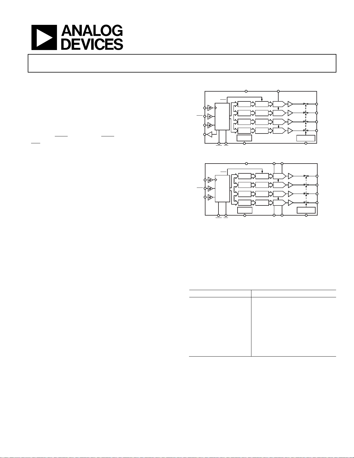
FUNCTIONAL BLOCK DIAGRAMS
DD
AD5064-1
SCLK
YNC
SDO
LDAC
INTERFACE
LOGIC AND
SHIFT
DIN
REGISTER
LDAC
CLR
INPUT
REGISTER
INPUT
REGISTER
INPUT
REGISTER
INPUT
REGISTER
POWER-ON
RESET
POR
REGISTER
REGISTER
REGISTER
REGISTER
Figure 1. AD5064-1 Functional Equivalent and Pin Compatible with AD5666
V
DD
INPUT
REGISTER
INPUT
REGISTER
INPUT
REGISTER
INPUT
REGISTER
POWER-ON
RESET
POR
REGISTER
REGISTER
REGISTER
REGISTER
SCLK
SYNC
AD5024/
AD5044/
AD5064
LDAC
INTERFACE
LOGIC AND
SHIFT
DIN
REGISTER
LDAC
CLR
Figure 2. AD5024/AD5044/AD5064 with Individual Reference Pins
DAC
DAC
DAC
DAC
DAC
DAC
DAC
DAC
REFIN
BUFFER
DAC A
BUFFER
DAC B
BUFFER
DAC C
BUFFER
DAC D
POWER-DOWN
A
B
REF
REF
BUFFER
DAC A
BUFFER
DAC B
BUFFER
DAC C
BUFFER
DAC D
POWER-DOWN
V
C V
D
REF
REF
LOGIC
GND
LOGIC
GND
V
A
OUT
B
V
OUT
C
V
OUT
D
V
OUT
06803-064
V
A
OUT
V
B
OUT
V
C
OUT
V
D
OUT
06803-001
GENERAL DESCRIPTION
The AD5024/AD5044/AD5064/AD5064-1 are low power, quad
12-/14-/16-bit buffered voltage output nanoDAC® converters
that offer relative accuracy specifications of 1 LSB INL and 1 LSB
DNL with the AD5024/AD5044/AD5064 individual reference
pin and the AD5064-1 common reference pin options. The
AD5024/AD5044/AD5064/AD5064-1 can operate from a single
4.5 V to 5.5 V supply. The AD5024/AD5044/AD5064/AD5064-1
also offer a differential accuracy specification of ±1 LSB. The
parts use a versatile 3-wire, low power Schmitt trigger serial
interface that operates at clock rates up to 50 MHz and is compatible with standard SPI, QSPI™, MICROWIRE™, and DSP interface
standards. Integrated reference buffers and output amplifiers are
also provided on-chip. The AD5024/AD5044/AD5064/AD5064-1
incorporate a power-on reset circuit that ensures the DAC
output powers up to zero scale or midscale and remains there
until a valid write takes place to the device. The AD5024/AD5044/
AD5064/AD5064-1 contain a power-down feature that reduces
the current consumption of the device to typically 400 nA at 5 V
and provides software selectable output loads while in powerdown mode. Total unadjusted error for the parts is <2 mV.
PRODUCT HIGHLIGHTS
1. Quad channel available in 14-/16-lead TSSOP packages.
2. 16-bit accurate, 1 LSB INL.
3. High speed serial interface with clock speeds up to 50 MHz.
4. Reset to known output voltage (zero scale or midscale).
Table 1. Related Devices
Part No. Description
AD5666
AD5025/AD5045/AD5065
AD5062, AD5063
AD5061 16-bit nanoDAC, 4 LSB INL, SOT-23
AD5040/AD5060
Quad,16-bit buffered DAC,
16 LSB INL, TSSOP
Dual, 16-bit buffered DACs,
1 LSB INL, TSSOP
16-bit nanoDAC, 1 LSB INL, SOT-23,
MSOP
14-/16-bit nanoDAC, 1 LSB INL,
SOT-23
Rev. C
Information furnished by Analog Devices is believed to be accurate and reliable. However, no
responsibility is assumed by Analog Devices for its use, nor for any infringements of patents or other
rights of third parties that may result from its use. Specifications subject to change without notice. No
license is granted by implication or otherwise under any patent or patent rights of Analog Devices.
Trademarks and registered trademarks are the property of their respective owners.
One Technology Way, P.O. Box 9106, Norwood, MA 02062-9106, U.S.A.
Tel: 781.329.4700 www.analog.com
Fax: 781.461.3113 ©2008–2010 Analog Devices, Inc. All rights reserved.
Page 2

AD5024/AD5044/AD5064
TABLE OF CONTENTS
Features .............................................................................................. 1
Applications ....................................................................................... 1
Functional Block Diagrams ............................................................. 1
General Description ......................................................................... 1
Product Highlights ........................................................................... 1
Revision History ............................................................................... 2
Specifications ..................................................................................... 3
AC Characteristics ........................................................................ 4
Timing Characteristics ................................................................ 5
Absolute Maximum Ratings ............................................................ 7
ESD Caution .................................................................................. 7
Pin Configurations and Function Descriptions ........................... 8
Typical Performance Characteristics ........................................... 10
Terminology .................................................................................... 17
Theory of Operation ...................................................................... 19
Digital-to-Analog Converter .................................................... 19
DAC Architecture ....................................................................... 19
Reference Buffer ......................................................................... 19
Output Amplifier ........................................................................ 19
Serial Interface ............................................................................ 19
Shift Register ............................................................................... 19
Modes of Operation ................................................................... 21
Power-On Reset .......................................................................... 22
Power-Down Modes .................................................................. 22
Clear Code Register ................................................................... 23
LDAC
Function .......................................................................... 23
Power Supply Bypassing and Grounding ................................ 24
Microprocessor Interfacing ....................................................... 25
Applications Information .............................................................. 26
Using a Reference as a Power Supply ....................................... 26
Bipolar Operation....................................................................... 26
Using the AD5024/AD5044/AD5064/AD5064-1 with a
Galvanically Isolated Interface ................................................. 26
Outline Dimensions ....................................................................... 27
Ordering Guide .......................................................................... 28
REVISION HISTORY
5/10—Rev. B to Rev. C
Changes to Power-On Reset Section ............................................ 22
6/09—Rev. A to Rev. B
Changes to Figure 1 .......................................................................... 1
3/09—Rev. 0 to Rev. A
Added 14-Lead TSSOP ...................................................... Universal
Added Figure 1; Renumbered Sequentially .................................. 1
Changes to Features Section, General Description Section,
Product Highlights Section, Figure 2, and Table 1 ....................... 1
Changes to Table 2 ............................................................................ 3
Changes to Timing Characteristics Section and Table 4 ............. 5
Added Circuit and Timing Diagrams Section and Figure 3 ....... 5
Added Figure 5 .................................................................................. 6
Changes to Figure 4 .......................................................................... 6
Added Figure 6 .................................................................................. 8
Added Table 6; Renumbered Sequentially .................................... 8
Changed Input Shift Register to Shift Register Throughout ...... 8
Changes to Table 7 ............................................................................. 9
Changes to Typical Performance Characteristics Section ........ 10
Changes to Terminology Section ................................................. 17
Changes to Digital-to-Analog Converter Section, Reference
Buffer Section, Output Amplifier Section, Serial Interface
Section, Shift Register Section, and Table 8 ................................ 19
Changes to Figure 47, Figure 48, and Figure 49 Captions ........ 20
Added Modes of Operation Section, Daisy-Chaining Section,
Table 10, and Table 11 .................................................................... 21
Changes to Table 13 and Power-Down Mode Section .............. 22
Changes to Table 16 ....................................................................... 24
Changes to Figure 52 to Figure 55 ................................................ 25
Changes to Bipolar Operation Section and Figure 56 to
Figure 58 .......................................................................................... 26
Added Figure 59 ............................................................................. 27
Updated Outline Dimensions ....................................................... 27
Changes to Ordering Guide .......................................................... 28
8/08—Revision 0: Initial Version
Rev. C | Page 2 of 28
Page 3

AD5024/AD5044/AD5064
SPECIFICATIONS
VDD = 4.5 V to 5.5 V, RL = 5 kΩ to GND, CL = 200 pF to GND, 2.5 V ≤ V
T
, unless otherwise noted.
MAX
≤ VDD, unless otherwise specified. All specifications T
REFIN
MIN
to
Table 2.
1, 2
Unit Conditions/Comments
+105°C
+125°C
= 2.5 V, VDD = 5.5 V
REF
All 1s loaded to DAC register, V
V
< VDD
REF
< VDD
REF
FSR/°C
change, R
V
DD
= 5 kΩ to GND or VDD
L
± 10%, DAC = full scale, V
< VDD
REF
option
Parameter
STATIC PERFORMANCE
1
B Grade
Min Typ Max Min Typ Max
3
A Grade
Resolution 16 16 Bits AD5064/AD5064-1
14 Bits AD5044
12 Bits AD5024
Relative Accuracy (INL)4 ±0.5 ±1 ±0.5 ±4 LSB AD5064/AD5064-1; TA = −40°C to
±0.5 ±2 ±0.5 ±4 LSB AD5064/AD5064-1; TA = −40°C to
±0.25 ±1 LSB AD5044
±0.12 ±0.5 LSB AD5024
Differential Nonlinearity (DNL)4
±0.2 ±1 ±0.2 ±1 LSB
Total Unadjusted Error ±2 ±2 mV V
Offset Error
Offset Error Temperature
Coefficient
4, 5
4, 6
Full-Scale Error4
Gain Error4
Gain Temperature Coefficient
DC Crosstalk
4, 6
±0.2 ±1.8 ±0.2 ±1.8 mV
±2 ±2 µV/°C
±0.01 ±0.07 ±0.01 ±0.07 % FSR
±0.005 ±0.05 ±0.005 ±0.05 % FSR
4, 6
±1 ±1 ppm
40 40 µV Due to single-channel, full-scale output
40 40 µV/mA Due to load current change
40 40 µV Due to powering down (per channel)
OUTPUT CHARACTERISTICS6
Output Voltage Range 0 VDD 0 VDD V
Capacitive Load Stability 1 1 nF RL = 5 kΩ, RL =100 kΩ, and RL = ∞
DC Output Impedance
Normal Mode 0.5 0.5 Ω
Power-Down Mode
Output Connected to
100 100 kΩ Output impedance tolerance ± 20 kΩ
100 kΩ Network
Output Connected to
1 1 kΩ Output impedance tolerance ± 400 Ω
1 kΩ Network
Short-Circuit Current 60 60 mA DAC = full scale, output shorted to GND
45 45 mA DAC = zero scale, output shorted to VDD
Power-Up Time7 4.5 4.5 µs
DC PSRR −92 −92 dB
REFERENCE INPUTS
Reference Input Range 2.2 VDD 2.2 VDD V
Reference Current 35 50 35 50 µA Per DAC channel; individual reference
140 160 140 160 µA Single reference option
Reference Input Impedance 120 120 kΩ Individual reference option
32 32 kΩ Single reference option
LOGIC INPUTS
Input Current8 ±1 ±1 µA
Input Low Voltage, V
Input High Voltage, V
Pin Capacitance6
0.8 0.8 V
INL
2.2 2.2 V
INH
4 4 pF
Rev. C | Page 3 of 28
Page 4
AD5024/AD5044/AD5064
1, 2
Unit Conditions/Comments
Parameter
B Grade
1
A Grade
Min Typ Max Min Typ Max
LOGIC OUTPUTS (SDO)9
Output Low Voltage, VOL 0.4 0.4 V I
Output High Voltage, VOH V
High Impedance Leakage
− 1 VDD − 1 I
DD
±0.002 ±1 ±0.002 ±1 A
= 2 mA
SINK
SOURCE
= 2 mA
Current
High Impedance Output
Capacitance
6
7 7 pF
POWER REQUIREMENTS
VDD 4.5 5.5 4.5 5.5 V DAC active, excludes load current
10
I
VIH = VDD, VIL = GND, Code = midscale
DD
Normal Mode 4 6 4 6 mA
All Power-Down Modes11 0.4 2 0.4 2 µA TA = −40°C to +105°C
30 30 µA TA = −40°C to +125°C
1
Temperature range is −40°C to +125°C, typical at 25°C.
2
A grade offered in AD5064 only.
3
Linearity and total unadjusted error are calculated using a reduced code range—AD5064/AD5064-1: Code 512 to Code 65,024; AD5044: Code 128 to Code 16,256;
AD5024: Code 32 to Code 4064. Output unloaded.
4
See the Terminology section.
5
Offset error calculated using a reduced code range—AD5064/AD5064-1: Code 512 to Code 65,024; AD5044: Code 128 to Code 16,256; AD5024: Code 32 to Code 4064.
Output unloaded
6
Guaranteed by design and characterization; not production tested.
7
Time to exit power-down mode to normal mode; 32nd clock edge to 90% of DAC midscale value, output unloaded.
8
Current flowing into individual digital pins. VDD = 5.5 V; V
9
AD5064-1 only.
10
Interface inactive. All DACs active. DAC outputs unloaded.
11
All four DACs powered down.
= 4.096 V; Code = midscale.
REF
AC CHARACTERISTICS
VDD = 4.5 V to 5.5 V, RL = 5 kΩ to GND, CL = 200 pF to GND, 2.5 V ≤ V
noted.
Table 3.
Parameter
Output Voltage Settling Time 5.8 8 µs
1, 2
Min Typ Max Unit Conditions/Comments3
¼ to ¾ scale and ¾ to ¼ scale settling to ±1 LSB, R
single-channel update
10.7 13 µs
¼ to ¾ scale and ¾ to ¼ scale settling to ±1 LSB, R
update
Slew Rate 1.5 V/µs
Digital-to-Analog Glitch Impulse 3 nV-sec 1 LSB change around major carry
Reference Feedthrough −90 dB V
Digital Feedthrough 0.1 nV-sec
Digital Crosstalk 1.9 nV-sec
Analog Crosstalk 2 nV-sec
DAC-to-DAC Crosstalk 3.5 nV-sec
AC Crosstalk 6 nV-sec
Multiplying Bandwidth 340 kHz V
Total Harmonic Distortion −80 dB V
Output Noise Spectral Density 64 nV/√Hz DAC code = 0x8400, frequency = 1 kHz
60 nV/√Hz DAC code = 0x8400, frequency = 10 kHz
Output Noise 6 V p-p 0.1 Hz to 10 Hz
1
Guaranteed by design and characterization; not production tested.
2
See the Terminology section.
3
Temperature range is −40°C to +125°C, typical at 25°C.
≤ VDD. All specifications T
REFIN
= 3 V ± 0.86 V p-p, frequency = 100 Hz to 100 kHz
REF
= 3 V ± 0.86 V p-p
REF
= 3 V ± 0.2 V p-p, frequency = 10 kHz
REF
MIN
to T
, unless otherwise
MAX
= 5 kΩ,
L
= 5 kΩ, all channel
L
Rev. C | Page 4 of 28
Page 5
AD5024/AD5044/AD5064
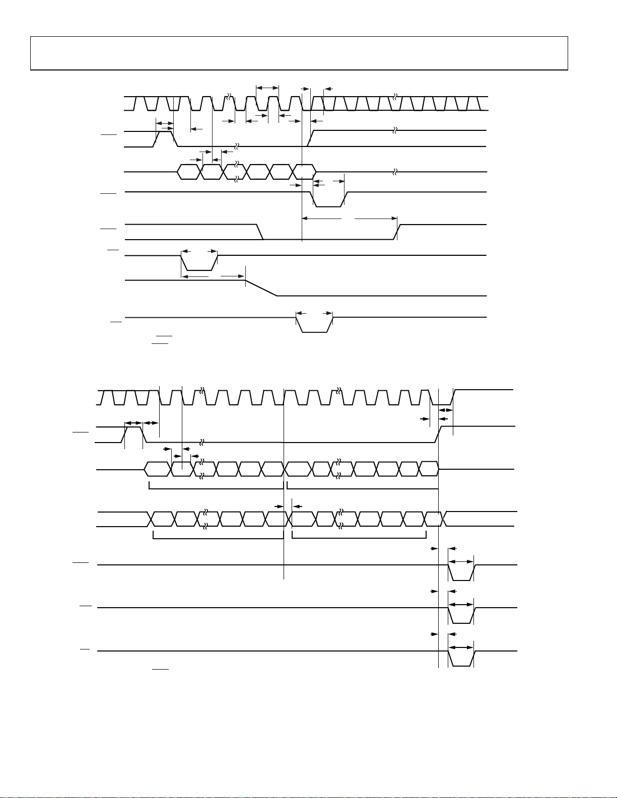
TIMING CHARACTERISTICS
All input signals are specified with tR = tF = 1 ns/V (10% to 90% of VDD) and timed from a voltage level of (VIL + VIH)/2. See Figure 4 and
Figure 5. V
Table 4.
Parameter1 Symbol Min Typ Max Unit
SCLK Cycle Time t1 20 ns
SCLK High Time t2 10 ns
SCLK Low Time t3 10 ns
SYNC to SCLK Falling Edge Setup Time
Data Setup Time t5 5 ns
Data Hold Time t6 5 ns
SCLK Falling Edge to SYNC Rising Edge
Minimum SYNC High Time (Single Channel Update)
Minimum SYNC High Time (All Channel Update)
SYNC Rising Edge to SCLK Fall Ignore
LDAC Pulse Width Low
SCLK Falling Edge to LDAC Rising Edge
CLR Minimum Pulse Width Low
SCLK Falling Edge to LDAC Falling Edge
CLR Pulse Activation Time
SCLK Rising Edge to SDO Valid t
SCLK Falling Edge to SYNC Rising Edge
SYNC Rising Edge to SCLK Rising Edge
SYNC Rising Edge to LDAC/CLR/PDL Falling Edge (Single Channel Update)
SYNC Rising Edge to LDAC/CLR/PDL Falling Edge (All Channel Update)
PDL Minimum Pulse Width Low
Power-up Time4 4.5 µs
1
Maximum SCLK frequency is 50 MHz at VDD = 4.5 V to 5.5 V. Guaranteed by design and characterization; not production tested.
2
Daisy-chain mode only.
3
Measured with the load circuit of Figure 3. t15 determines the maximum SCLK frequency in daisy-chain mode. AD5064-1 only.
4
Time to exit power-down mode to normal mode of AD5024/AD5044/AD5064/AD5064-1, 32nd clock edge to 90% of DAC midscale value, with output unloaded.
Circuit and Timing Diagrams
= 4.5 V to 5.5 V. All specifications T
DD
MIN
to T
, unless otherwise noted.
MAX
t
17 ns
4
t
5 30 ns
7
t
2 µs
8
t
8 µs
8
t
17 ns
9
t
20 ns
10
t
20 ns
11
t
10 ns
12
t
10 ns
13
t
10.6 µs
14
2, 3
15
2
t
5 ns
16
2
t
8 ns
17
2
t
2 µs
18
2
t
8 µs
18
t
19
22 ns
20 ns
2mA I
OL
TO OUTPUT
PIN
50pF
C
L
2mA I
OH
VOH (MIN) + VOL (MAX)
2
06803-002
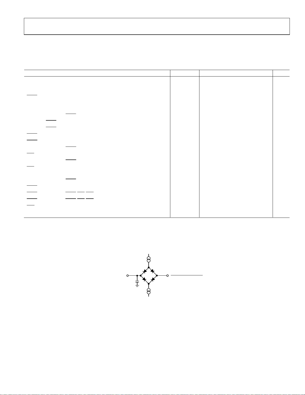
Figure 3. Load Circuit for Digital Output (SDO) Timing Specifications
Rev. C | Page 5 of 28
Page 6
AD5024/AD5044/AD5064
2
SCLK
t
8
SYNC
DIN
1
LDAC
2
LDAC
CLR
V
OUT
PDL
1
ASYNCHRONOUS LDAC UPDAT E MODE.
SYNCHRONOUS LDAC UPDAT E MODE.
DB31
t
4
t
6
t
5
t
12
t
14
t
1
t
t
3
2
DB0
t
9
t
7
t
10
t
13
t
11
t
19
06803-003
Figure 4. Serial Write Operation
SCLK
t8t
4
SYNC
t
5
t
6
DIN
INPUT WORD FOR DAC N
SDO
UNDEFINED
1
LDAC
CLR
PDL
1
IF IN DAISY -CHAIN MODE, LDAC MUST BE USED ASYNCHRONOUSLY.
32 64
t
16
DB0DB31
DB31
INPUT WO RD FOR DAC N + 1
t
15
DB31
INPUT WORD FOR DAC N
t
t
t
DB0
DB0
18
18
18
t
17
t
10
t
12
t
19
06803-004
Figure 5. Daisy-Chain Timing Diagram
Rev. C | Page 6 of 28
Page 7
AD5024/AD5044/AD5064
ABSOLUTE MAXIMUM RATINGS
TA = 25°C, unless otherwise noted.
Table 5.
Parameter Rating
VDD to GND −0.3 V to +7 V
Digital Input Voltage to GND −0.3 V to VDD + 0.3 V
V
to GND −0.3 V to VDD + 0.3 V
OUT
V
to GND −0.3 V to VDD + 0.3 V
REF
Operating Temperature Range
Industrial −40°C to +125°C
Storage Temperature Range −65°C to +150°C
Junction Temperature (TJ
TSSOP Package
Power Dissipation (TJ
θJA Thermal Impedance 113°C/W
Reflow Soldering Peak Temperature
Pb-Free 260°C
) 150°C
MAX
− TA)/θJA
MAX
Stresses above those listed under Absolute Maximum Ratings
may cause permanent damage to the device. This is a stress
rating only; functional operation of the device at these or any
other conditions above those indicated in the operational
section of this specification is not implied. Exposure to absolute
maximum rating conditions for extended periods may affect
device reliability.
ESD CAUTION
Rev. C | Page 7 of 28
Page 8
AD5024/AD5044/AD5064
PIN CONFIGURATIONS AND FUNCTION DESCRIPTIONS
LDAC
SYNC
V
OUT
V
OUT
POR
V
REFIN
V
DD
A
C
1
2
3
AD5064-1
4
TOP VIEW
5
(Not to Scale)
6
7
14
SCLK
DIN
13
12
GND
B
V
11
OUT
D
V
10
OUT
9
CLR
8
SDO
6803-065
Figure 6. 14-Lead TSSOP (RU-14)
Table 6. Pin Function Descriptions
Pin No. Mnemonic Description
1
LDAC can be operated in two modes, asynchronously and synchronously, as shown in . Pulsing
LDAC
this pin low allows any or all DAC registers to be updated if the input registers have new data. This allows
all DAC outputs to simultaneously update. This pin can also be tied permanently low in standalone mode.
When daisy-chain mode is enabled, this pin cannot be tied permanently low; the
used in asynchronous LDAC update mode, as shown in , and the Figure 5 LDAC pin must be brought
high after pulsing.
2
Active Low Control Input. This is the frame synchronization signal for the input data. When SYNC goes
SYNC
low, it powers on the SCLK and DIN buffers and enables the shift register. Data is transferred in on the
falling edges of the next 32 clocks. If SYNC is taken high before the 32nd falling edge, the rising edge of
SYNC
acts as an interrupt and the write sequence is ignored by the device.
3 VDD
Power Supply Input. These parts can be operated from 4.5 V to 5.5 V, and the supply should be decoupled
with a 10 µF capacitor in parallel with a 0.1 µF capacitor to GND.
4 V
5 V
6 POR
A Analog Output Voltage from DAC A. The output amplifier has rail-to-rail operation.
OUT
C Analog Output Voltage from DAC C. The output amplifier has rail-to-rail operation.
OUT
Power-On Reset Pin. Tying this pin to GND powers up all four DACs to zero scale. Tying this pin to V
powers up all four DACs to midscale.
7 V
8 SDO
This is a common pin for reference input for DAC A, DAC B, DAC C, and DAC D.
REFIN
Serial Data Output. Can be used to daisy-chain a number of AD5064-1 devices together. The serial data
is transferred on the rising edge of SCLK and is valid on the falling edge of the clock.
9
Asynchronous Clear Input. The CLR input is falling edge sensitive. When CLR is low, all LDAC pulses are
CLR
ignored. When CLR
is activated, the input register and the DAC register are updated with the data
contained in the clear code register—zero, midscale, or full scale. Default setting clears the output to 0 V.
10 V
11 V
D Analog Output Voltage from DAC D. The output amplifier has rail-to-rail operation.
OUT
B Analog Output Voltage from DAC B. The output amplifier has rail-to-rail operation.
OUT
12 GND Ground Reference Point for All Circuitry on the Part.
13 DIN
Serial Data Input. This device has a 32-bit shift register. Data is clocked into the shift register on the
falling edge of the serial clock input.
14 SCLK
Serial Clock Input. Data is clocked into the shift register on the falling edge of the serial clock input. Data
can be transferred at rates of up to 50 MHz.
Figure 4
LDAC
pin should be
DD
Rev. C | Page 8 of 28
Page 9
AD5024/AD5044/AD5064
V
V
LDAC
SYNC
V
V
REF
V
REF
OUT
OUT
POR
DD
B
A
A
C
1
2
3
AD5024/
AD5044/
4
AD5064
5
TOP VIEW
6
(Not to Scale)
7
8
SCLK
16
15
DIN
14
GND
B
V
13
OUT
D
V
12
OUT
V
D
11
REF
10
CLR
9
C
V
REF
06803-005
Figure 7. 16-Lead TSSOP (RU-16) Pin Configuration
Table 7. Pin Function Descriptions
Pin No. Mnemonic Description
1
LDAC can be operated in two modes, asynchronously and synchronously, as shown in . Pulsing
LDAC
this pin low allows any or all DAC registers to be updated if the input registers have new data. This allows
all DAC outputs to simultaneously update. This pin can also be tied permanently low in standalone mode.
2
Active Low Control Input. This is the frame synchronization signal for the input data. When SYNC goes
SYNC
low, it powers on the SCLK and DIN buffers and enables the shift register. Data is transferred in on the
falling edges of the next 32 clocks. If SYNC
is taken high before the 32nd falling edge, the rising edge of
SYNC acts as an interrupt and the write sequence is ignored by the device.
3 VDD
Power Supply Input. These parts can be operated from 4.5 V to 5.5 V, and the supply should be decoupled
with a 10 µF capacitor in parallel with a 0.1 µF capacitor to GND.
4 V
5 V
6 V
7 V
8 POR
B DAC B Reference Input. This is the reference voltage input pin for DAC B.
REF
A DAC A Reference Input. This is the reference voltage input pin for DAC A.
REF
A Analog Output Voltage from DAC A. The output amplifier has rail-to-rail operation.
OUT
C Analog Output Voltage from DAC C. The output amplifier has rail-to-rail operation.
OUT
Power-On Reset. Tying this pin to GND powers up the part to 0 V. Tying this pin to V
part to midscale.
9 V
10
C DAC C Reference Input. This is the reference voltage input pin for DAC C.
REF
Asynchronous Clear Input. The CLR input is falling edge sensitive. When CLR is low, all LDAC pulses are
CLR
ignored. When CLR
is activated, the input register and the DAC register are updated with the data
contained in the clear code register—zero, midscale, or full scale. Default setting clears the output to 0 V.
11 V
12 V
13 V
D DAC D Reference Input. This is the reference voltage input pin for DAC D.
REF
D Analog Output Voltage from DAC D. The output amplifier has rail-to-rail operation.
OUT
B Analog Output Voltage from DAC B. The output amplifier has rail-to-rail operation.
OUT
14 GND Ground Reference Point for All Circuitry on the Part.
15 DIN
Serial Data Input. This device has a 32-bit shift register. Data is clocked into the shift register on the
falling edge of the serial clock input.
16 SCLK
Serial Clock Input. Data is clocked into the shift register on the falling edge of the serial clock input. Data
can be transferred at rates of up to 50 MHz.
Figure 4
powers up the
DD
Rev. C | Page 9 of 28
Page 10

AD5024/AD5044/AD5064
TYPICAL PERFORMANCE CHARACTERISTICS
1.0
VDD = 5V
V
= 4.096V
REF
0.8
T
= 25°C
A
0.6
0.4
0.2
0
INL (LSB)
–0.2
–0.4
–0.6
–0.8
–1.0
512 16,640 32,768 48, 896 65, 024
DAC CODE
Figure 8. AD5064/AD5064-1 INL
06803-019
1.0
VDD = 5V
= 4.096V
V
REF
0.8
= 25°C
T
A
0.6
0.4
0.2
0
DNL (LSB)
–0.2
–0.4
–0.6
–0.8
–1.0
512 16,640 32, 768 48,896 65,024
DAC CODE
Figure 11. AD5064/AD5064-1 DNL
06803-022
1.0
VDD = 5V
V
= 4.096V
0.8
REF
T
= 25°C
A
0.6
0.4
0.2
0
INL (LSB)
–0.2
–0.4
–0.6
–0.8
–1.0
0 512 1024 1536 2048 2560 3072 3584 4096
DAC CODE
Figure 9. AD5044 INL
1.0
VDD = 5V
V
= 4.096V
0.8
REF
T
= 25°C
A
0.6
0.4
0.2
0
INL (LSB)
–0.2
–0.4
–0.6
–0.8
–1.0
0 512 1024 1536 2048 2560 3072 3584 4096
DAC CODE
Figure 10. AD5024 INL
1.0
VDD = 5V
= 4.096V
V
0.8
REF
= 25°C
T
A
0.6
0.4
0.2
0
DNL (LSB)
–0.2
–0.4
–0.6
–0.8
06803-020
–1.0
0 4096 8192 12,288 16,384
DAC CODE
06803-023
Figure 12. AD5044 DNL
1.00
VDD = 5V
= 4.096V
V
REF
0.75
= 25°C
T
A
0.50
0.25
0
DNL (LSB)
–0.25
–0.50
–0.75
06803-021
–1.00
0 4096 8192 12, 288 16,384
DAC CODE
06803-024
Figure 13. AD5024 DNL
Rev. C | Page 10 of 28
Page 11

AD5024/AD5044/AD5064
0.20
VDD = 5V
V
= 4.096V
REF
0.15
T
= 25°C
A
0.10
0.05
0
TUE (mV)
–0.05
–0.10
–0.15
–0.20
512 16,640 32, 768 48,896 65,024
DAC CODE
Figure 14. Total Unadjusted Error (TUE)
06803-025
1.2
T
= 25°C
A
1.0
0.8
0.6
0.4
0.2
0
–0.2
TUE (mV)
–0.4
–0.6
–0.8
–1.0
–1.2
2.0
MAX TUE @ VDD = 5.5V
MIN TUE @ VDD = 5.5V
06803-028
5.55.04. 54.03.53.02.5
REFERENCE VO LTAGE (V)
Figure 17. TUE vs. Reference Input Voltage
1.6
TA = 25°C
1.4
1.2
1.0
0.8
0.6
0.4
0.2
0
–0.2
–0.4
INL ERROR (LSB)
–0.6
–0.8
–1.0
–1.2
–1.4
–1.6
2.0
MAX INL ERROR @ VDD = 5.5V
MIN INL E RROR @ VDD = 5.5V
06803-026
5.55.04. 54.03.53.02.5
REFERENCE VO LTAGE (V)
Figure 15. INL vs. Reference Input Voltage
1.6
TA = 25°C
1.4
1.2
1.0
0.8
0.6
0.4
0.2
0
–0.2
–0.4
DNL ERROR (LSB)
–0.6
–0.8
–1.0
–1.2
–1.4
–1.6
2.0
MAX DNL ERROR @ VDD = 5.5V
MIN DNL ERROR @ V
REFERENCE VOL TAGE (V)
DD
= 5.5V
06803-027
5.55.04. 54.03.53.02.5
Figure 16. DNL vs. Reference Input Voltage
0.015
0.010
0.005
0
–0.005
GAIN ERROR (%FS R)
–0.010
–0.015
–60 –20 40 80 140
DAC A
DAC B
VDD= 5.5V
= 4.096V
V
REF
–40 0 20 60 100
TEMPERATURE ( °C)
DAC D
DAC C
Figure 18. Gain Error vs. Temperature
0.6
0.5
0.4
0.3
0.2
0.1
0
–0.1
OFFSET ERROR (mV)
–0.2
–0.3
–0.4
–60 0 40 80 140
DAC C
DAC D
DAC A
DAC B
–40 20–20 60 100 120
TEMPERATURE (ºC)
VDD= 5.5V
V
Figure 19. Offset Error vs. Temperature
REF
120
= 4.096V
06803-029
06803-030
Rev. C | Page 11 of 28
Page 12

AD5024/AD5044/AD5064
0.2
0.1
V
REF
T
A
= 4.096V
= 25°C
10
8
VDD = 5.5V
V
= 4.096
REF
T
= 25°C
A
0
ERROR (%FSR)
GAIN ERROR
FULL-SCAL E ERROR
–0.1
–0.2
4.50 4. 75 5. 00 5. 25 5. 50
VDD (V)
Figure 20. Gain Error and Full-Scale Error vs. Supply Voltage
0.12
V
= 4.096V
REF
T
= 25°C
A
0.09
0.06
OFFSET ERROR (mV)
0.03
0
4.50 4. 75 5. 00 5. 25 5. 50
VDD (V)
Figure 21. Offset Error Voltage vs. Supply Voltage
6
(mA)
DD
I
4
2
06803-031
0
0 10,000 20,000 30,000 40,000 50,000 60,000 70,000
DAC CODE
06803-034
Figure 23. Supply Current vs. Code
10
VDD = 5.5V
V
= 4.096
REF
CODE = MIDSCALE
8
6
(mA)
DD
I
4
2
06803-032
0
–40 –20 0 20 40 60 80 100 120
TEMPERATURE (° C)
06803-035
Figure 24. Supply Current vs. Temperature
40
MEAN: 4.11699
SD: 0.0544403
35
LIMITS: LOW: 3 HIGH: 4.3
CPk: LOW: 6.84 HIGH: 1.12
= 4.096V
V
REF
30
= 25°C
T
A
CODE = MIDSCALE
25
20
HITS
15
10
5
0
3.9 4.0 4.1 4.2 4. 3
Figure 22. IDD Histogram, VDD = 5.0 V
I
DD P OWER-UP
(mA)
06803-033
Rev. C | Page 12 of 28
10
VDD = 5.5V
= 4.096
V
REF
T
= 25°C
A
8
6
(mA)
DD
I
4
2
0
4.5 4.6 4.7 4.8 4.9 5.0 5.1 5. 2 5.3 5. 4 5.5
SUPPLY VOLTAGE (V)
Figure 25. Supply Current vs. Supply Voltage
06803-036
Page 13

AD5024/AD5044/AD5064
10
VDD = 5.5V
V
= 4.096
REF
T
= 25°C
A
8
6
(mA)
DD
I
4
2
0
012345
DIGITAL INPUT VOLTAGE (V)
Figure 26. Supply Current vs. Digital Input Voltage
5.0
4.5
4.0
3.5
3.0
2.5
2.0
1.5
OUTPUT VOLTAGE (V)
VDD = 5V, V
= 25ºC
T
A
1/4 SCALE TO 3/4 SCALE
3/4 SCALE TO 1/4 SCALE
OUTPUT LOADED WITH 5kΩ
AND 200pF TO GND
REF
= 4.096V
1.0
0.5
0
02468101214
TIME (µs)
Figure 27. Settling Time
06803-037
06803-038
V
= 4.096V
REF
T
= 25°C
A
OUTPUT UNLO ADED
1
V
DD
DAC A
3
CH1 2V CH3 2V M2ms A CH1 2.52V
T 20.4%
Figure 29. Power-On Reset to Midscale
CH1 = SCLK
1
CH2 = V
OUT
2
VDD = 5V
POWER-UP T O MIDSCAL E
OUTPUT UNL OADED
CH1 5V CH2 500mV M2µ s A CH2 1. 2V
T 55%
Figure 30. Exiting Power-Down to Midscale
06803-040
06803-041
V
= 4.096V
REF
T
= 25°C
A
1
3
CH1 2V CH3 2V M2ms A CH1 2.52V
T 20.4%
V
DD
DAC A
Figure 28. Power-On Reset to 0 V
06803-039
Rev. C | Page 13 of 28
6
5
4
CODE = 0x8000 TO 0x7FFF
OUTPUT UNLO ADED WITH 5kΩ
3
2
1
0
GLITCH AMPLITUDE (mV)
–1
–2
–3
0 2.5 5.0 7.5 10.0
TIME (μs)
Figure 31. Digital-to-Analog Glitch Impulse
VDD = 5V
= 4.096V
V
REF
T
A
AND 200pF
= 25°C
06803-042
Page 14

AD5024/AD5044/AD5064
V
7
VDD = 5V, V
6
T
= 25ºC
A
5
4
3
2
1
0
–1
GLITCH AMPL ITUDE (mV)
–2
–3
–4
0 2.5 5.0 7.5 10.0
REF
= 4.096V
TIME (μs)
Figure 32. Analog Crosstalk
7
6
5
4
3
2
1
0
–1
GLITCH AMPLITUDE (mV)
–2
–3
–4
0 2.5 5.0 7.5 10.0
TIME (μs)
VDD = 5V, V
T
= 25°C
A
Figure 33. DAC-to-DAC Crosstalk
REF
06803-043
= 4.096V
06803-044
0
–10
–20
–30
–40
–50
LEVEL (dB)
–60
OUT
V
–70
–80
–90
–100
5 10 30 40 55
20 50
VDD= 5V,
= 25ºC
T
A
DAC LOADED WITH MIDSCALE
= 3.0V ± 200mV p -p
V
REF
FREQUENCY (kHz)
Figure 35. Total Harmonic Distortion
24
VDD = 5V, V
= 25°C
T
22
A
1/4 SCALE T O 3/4 SCALE
WITHIN ±1LSB
20
18
16
14
12
SETTLING TIME (μs)
10
8
6
4
01 5 7 10
= 3.0V
REF
3924
CAPACITANCE (nF)
6
Figure 36. Settling Time vs. Capacitive Load
06803-046
8
06803-047
VDD = 5V, V
= 25ºC
T
A
DAC LOADED WI TH MIDSCALE
1μV/DI
= 4.096V
REF
4s/DIV
Figure 34. 0.1 Hz to 10 Hz Output Noise Plot
CLR
CLR
DAC A
06803-048
1
2
VDD = 5V
V
= 4.096V
REF
T
= 25ºC
06803-045
A
CH1 5V CH2 2V M2µs A CH1 2.5V
T 11%
Figure 37. Hardware
Rev. C | Page 14 of 28
Page 15

AD5024/AD5044/AD5064
10
0
–10
–20
–30
ATTENUATIO N (dB)
–40
CH A
CH B
–50
CH C
CH D
3dB POINT
–60
10 100 1000 10000
FREQUENCY (kHz)
Figure 38. Multiplying Bandwidth
5.0
4.5
4.0
3.5
3.0
2.5
2.0
1.5
OUTPUT VO LTAGE (V)
1.0
0.5
0
0 2 4 6 8 10 12 14
VDD = 5V, V
T
1/4 SCALE TO 3/4 SCALE
3/4 SCALE TO 1/4 SCALE
OUTPUT L OADED WIT H 5kΩ
AND 200pF TO GND
TIME (µs)
= 25°C
A
REF
= 4.096V
Figure 39. Typical Output Slew Rate
06803-049
06803-050
0.10
CODE = MIDSCAL E
V
= 5V, V
DD
0
–25 –20 –15 –10 –5 0 5 10 15 20 25 30
(V)
ΔV
0.08
0.06
0.04
0.02
OUT
–0.02
–0.04
–0.06
–0.08
–0.10
REF
= 4.096V
I
OUT
06803-052
(mA)
Figure 41. Typical Current Limiting Plot
TA = 25°C
V
= 5V, V
DD
CH1 50mV CH2 5V M4µs A CH2 1.2V
REF
= 4.096V
DAC A 295mV p-p
06803-053
T 8. 6%
Figure 42. Glitch Upon Entering Power-Down (1 kΩ to GND) from Zero Scale,
No Load
0.0010
CODE = MIDSCALE
= 5V, V
V
DD
0.0008
0.0006
0.0004
0.0002
0
ΔVOLTAGE (V)
–0.0002
–0.0004
–0.0006
–0.0008
–25 –20 –15 –10 –5 0 5 10 15 20 25 30
REF
= 4.096V
CURRENT (mA)
Figure 40. Typical Output Load Regulation
06803-051
Figure 43. Glitch Upon Entering Power-Down (1 kΩ to GND) from Zero Scale,
Rev. C | Page 15 of 28
TA = 25°C
V
= 5V, V
DD
CH1 50mV CH2 5V M4µs A CH2 1.2V
REF
= 4.096V
DAC A 200mV p-p
SCLK
T 8. 6%
5 kΩ/200 pF Load
06803-054
Page 16

AD5024/AD5044/AD5064
VDD = 5V,V
T
= 25°C
A
REF
= 4.096V
DAC A 129mV p-p
TA = 25°C
V
= 5V, V
DD
REF
= 4.096V
DAC A 170mV p-p
SCLK
CH1 20mV CH2 5V M4µs A CH2 1.2V
T 8.6%
06803-055
Figure 44. Glitch Upon Exiting Power-Down (1 kΩ to GND) to Zero Scale,
No Load
SCLK
CH1 20mV CH2 5V M4µs A CH2 1.2V
T 8.6%
Figure 45. Glitch Upon Exiting Power-Down (1 kΩ to GND) to Zero Scale,
5 kΩ/200 pF Load
06803-056
Rev. C | Page 16 of 28
Page 17

AD5024/AD5044/AD5064
TERMINOLOGY
Relative Accuracy (INL)
For the DAC, relative accuracy, or integral nonlinearity (INL),
is a measure of the maximum deviation in LSBs from a straight
line passing through the endpoints of the DAC transfer function.
Figure 8, Figure 9, and Figure 10 show plots of typical INL vs.
code.
Differential Nonlinearity (DNL)
DNL is the difference between the measured change and the
ideal 1 LSB change between any two adjacent codes. A specified
differential nonlinearity of ±1 LSB maximum ensures monotonicity. This DAC is guaranteed monotonic by design. Figure 11,
Figure 12, and Figure 13 show plots of typical DNL vs. code.
Offset Error
Offset error is a measure of the difference between the actual
V
and the ideal V
OUT
, expressed in millivolts in the linear
OUT
region of the transfer function. Offset error is calculated using
a reduced code range—AD5064/AD5604-1: Code 512 to Code
65,024; AD5044: Code 128 to Code 16,256; AD5024: Code 32 to
Code 4064, with output unloaded. Offset error can be negative or
positive and is expressed in millivolts.
Gain Error
Gain error is a measure of the span error of the DAC. It is the
deviation in slope of the DAC transfer characteristic from the
ideal, expressed as a percentage of the full-scale range.
Offset Error Temperature Coefficient
Offset error temperature coefficient is a measure of the change
in offset error with a change in temperature. It is expressed in
microvolts per degree Celsius.
Gain Temperature Coefficient
Gain error drift is a measure of the change in gain error with
changes in temperature. It is expressed in parts per million of
full-scale range per degree Celsius.
Full-Scale Error
Full-scale error is a measure of the output error when full-scale
code (0xFFFF) is loaded into the DAC register. Ideally, the
output should be V
percentage of the full-scale range. Measured with V
− 1 LSB. Full-scale error is expressed as a
REF
< VDD.
REF
Digital-to-Analog Glitch Impulse
Digital-to-analog glitch impulse is the impulse injected into the
analog output when the input code in the DAC register changes
state. It is normally specified as the area of the glitch in nanovoltseconds and is measured when the digital input code is changed
by 1 LSB at the major carry transition (0x7FFF to 0x8000). See
Figure 31.
DC Power Supply Rejection Ratio (PSRR)
PSRR indicates how the output of the DAC is affected by changes
in the supply voltage. PSRR is the ratio of the change in V
a change in V
in decibels. V
Measured with V
for full-scale output of the DAC. It is measured
DD
is held at 2.5 V, and VDD is varied by ±10%.
REF
< VDD.
REF
OUT
to
DC Crosstalk
DC crosstalk is the dc change in the output level of one DAC in
response to a change in the output of another DAC. It is measured
with a full-scale output change on one DAC (or soft power-down
and power-up) while monitoring another DAC kept at midscale.
It is expressed in microvolts.
DC crosstalk due to load current change is a measure of the
impact that a change in load current on one DAC has to another
DAC kept at midscale. It is expressed in microvolts per milliamp.
Reference Feedthrough
Reference feedthrough is the ratio of the amplitude of the signal
at the DAC output to the reference input when the DAC output
is not being updated (that is,
LDAC
is high). It is expressed in
decibels.
Digital Feedthrough
Digital feedthrough is a measure of the impulse injected into
the analog output of a DAC from the digital input pins of the
device, but it is measured when the DAC is not being written
SYNC
to (
held high). It is specified in nanovolt-seconds and
measured with one simultaneous data and clock pulse loaded
to the DAC.
Digital Crosstalk
Digital crosstalk is the glitch impulse transferred to the output
of one DAC at midscale in response to a full-scale code change
(all 0s to all 1s or vice versa) in the input register of another
DAC. It is measured in standalone mode and is expressed in
nanovolt-seconds.
Analog Crosstalk
Analog crosstalk is the glitch impulse transferred to the output
of one DAC due to a change in the output of another DAC. It is
measured by loading one of the input registers with a full-scale
code change (all 0s to all 1s or vice versa) while keeping
high, and then pulsing
LDAC
low and monitoring the output of
LDAC
the DAC whose digital code has not changed. The area of the
glitch is expressed in nanovolt-seconds.
Rev. C | Page 17 of 28
Page 18

AD5024/AD5044/AD5064
DAC-to-DAC Crosstalk
DAC-to-DAC crosstalk is the glitch impulse transferred to the
output of one DAC due to a digital code change and subsequent
output change of another DAC. This includes both digital and
analog crosstalk. It is measured by loading one of the DACs
with a full-scale code change (all 0s to all 1s or vice versa) with
LDAC
low and monitoring the output of another DAC. The
energy of the glitch is expressed in nanovolt-seconds.
Multiplying Bandwidth
The multiplying bandwidth is a measure of the finite bandwidth
of the amplifiers within the DAC. A sine wave on the reference
(with full-scale code loaded to the DAC) appears on the output.
The multiplying bandwidth, expressed in kilohertz, is the
frequency at which the output amplitude falls to 3 dB below
the input.
Total Harmonic Distortion (THD)
Total harmonic distortion is the difference between an ideal
sine wave and its attenuated version using the DAC. The sine
wave is used as the reference for the DAC, and the THD is a
measure of the harmonics present on the DAC output. It is
measured in decibels.
Rev. C | Page 18 of 28
Page 19

AD5024/AD5044/AD5064
V
THEORY OF OPERATION
DIGITAL-TO-ANALOG CONVERTER
The AD5024/AD5044/AD5064/AD5064-1 are single 12-/14-/
16-bit, serial input, voltage output DACs with an individual
reference pin. The AD5064-1 model (see the Ordering Guide)
is a 16-bit, serial input, voltage output DAC that is identical to
other AD5064 models but with a single reference pin for all
DACs. The parts operate from supply voltages of 4.5 V to 5.5 V.
Data is written to the AD5024/AD5044/AD5064/AD5064-1 in a
32-bit word format via a 3-wire serial interface. The AD5024/
AD5044/AD5064/AD5064-1 incorporate a power-on reset circuit
that ensures that the DAC output powers up to a known output
state. The devices also have a software power-down mode that
reduces the typical current consumption to typically 400 nA.
Because the input coding to the DAC is straight binary, the ideal
output voltage when using an external reference is given by
REFIN
⎛
×=
⎟
⎜
N
2
⎠
⎝
OUT
VV
D
⎞
where:
D is the decimal equivalent of the binary code that is loaded to
the DAC register (0 to 65,535 for the 16-bit AD5064).
N is the DAC resolution.
DAC ARCHITECTURE
The DAC architecture of the AD5064 consists of two matched
DAC sections. A simplified circuit diagram is shown in Figure 46.
The four MSBs of the 16-bit data word are decoded to drive
15 switches, E1 to E15. Each of these switches connects one of
15 matched resistors to either GND or the V
buffer output.
REF
The remaining 12 bits of the data-word drive the S0 to S11
switches of a 12-bit voltage mode R-2R ladder network.
OUT
2R
2R
2R
2R
S1
S0
V
REF
12-BIT R-2R L ADDER FOUR MSBs DECODED IN TO
Figure 46. DAC Ladder Structure
2R
2R
E1
S11
15 EQUAL SEGMENTS
E2
2R
E15
REFERENCE BUFFER
The AD5024/AD5044/AD5064/AD5064-1 operate with an external reference. For most models, each DAC has a dedicated voltage
reference pin. The AD5064-1 model has a single voltage reference
pin for all DACs. The reference input pin has an input range of
2.2 V to V
provide a reference for the DAC core.
. This input voltage is then buffered internally to
DD
06803-006
OUTPUT AMPLIFIER
The output buffer amplifier can generate rail-to-rail voltages
on its output, which gives an output range of 0 V to V
DD
. The
amplifier is capable of driving a load of 5 kΩ in parallel with
200 pF to GND. The slew rate is 1.5 V/µs with a ¼ to ¾ scale
settling time of 5.8 µs.
SERIAL INTERFACE
The AD5024/AD5044/AD5064/AD5064-1 have a 3-wire serial
interface (
SYNC
, SCLK, and DIN) that is compatible with SPI,
QSPI, and MICROWIRE interface standards as well as most
DSPs. See for a timing diagram of a typical write
Figure 4
sequence. The AD5064-1 model contains an SDO pin to allow
the user to daisy-chain multiple devices together (see the
Chaining
section).
Daisy-
SHIFT REGISTER
The AD5024/AD5044/AD5064/AD5064-1 shift register is 32 bits
wide. The first four bits are don’t cares. The next four bits are the
command bits, C3 to C0 (see Tabl e 8), followed by the 4-bit
DAC address bits, A3 to A0 (see Tab l e 9 ), and finally the bit
data-word. The data-word comprises 12-bit, 14-bit, or 16-bit input
code, followed by eight, six, or four don’t care bits for the AD5024,
AD5044, and AD5064/AD5064-1, respectively (see Figure 47,
Figure 48, and Figure 49). These data bits are transferred to the
DAC register on the 32
executed on individually selected DAC channels or on all DACs.
Table 8. Command Definitions
Command
C3 C2 C1 C0 Description
0 0 0 0 Write to Input Register n
0 0 0 1 Update DAC Register n
0 0 1 0 Write to Input Register n, update all
0 0 1 1 Write to and update DAC Channel n
0 1 0 0 Power down/power up DAC
0 1 0 1 Load clear code register
0 1 1 0
0 1 1 1 Reset (power-on reset)
1 0 0 0 Set up DCEN register1 (daisy-chain enable)
1 0 0 1 Reserved
1 1 1 1 Reserved
1
Available in the AD5064-1 14-lead TSSOP package only.
Table 9. Address Commands
Address (n)
A3 A2 A1 A0
0 0 0 0 DAC A
0 0 0 1 DAC B
0 0 1 0 DAC C
0 0 1 1 DAC D
1 1 1 1 All DACs
nd
falling edge of SCLK. Commands can be
LDAC
(software
LDAC
Load
)
register
Selected DAC Channel
Rev. C | Page 19 of 28
Page 20

AD5024/AD5044/AD5064
DB31 (MSB) DB0 (LSB)
X
XXX
C3 C2 C1 C0 A3 A2 A1 A0 D11 D10 D9 D8 D7 D6 D5 D4 D3 D2 D1 D0 X X X XXXXX
DATA BITS
ADDRESS BIT SCOMMAND BITS
Figure 47. AD5024 Shift Register Content
DB31 (MSB) DB0 (LSB)
X
XXX
C3 C2 C1 C0 A3 A2 A1 A0 D13 D12 D11 D10 D9 D8 D7 D6 D5 D4 D3 D2 D1 D0 X X XXX X
DATA BITS
ADDRESS BITSCOMMAND BITS
Figure 48. AD5044 Shift Register Content
DB31 (MSB) DB0 (LSB)
X
XXX
C3 C2 C1 C0 A3 A2 A1 A0 D15 D14 D13 D12 D11 D10 D9 D8 D7 D6 D5 D4 D3 D2 D1 D0 X X X X
DATA BITS
ADDRESS BITSCO MMAND BITS
Figure 49. AD5064/AD5064-1 Shift Register Content
06803-009
06803-008
06803-007
SCLK
SYNC
DIN
SYNC HIGH BEF ORE 32
DB31 DB0
INVALID WRITE SEQUENCE:
ND
FALLING EDGE
Figure 50.
SYNC
Interrupt Facility
DB31 DB0
VALID WRI TE SEQUE NCE, OUTP UT UPDATES
ON THE 32
ND
FALLING EDGE
06803-010
Rev. C | Page 20 of 28
Page 21

AD5024/AD5044/AD5064
MODES OF OPERATION
There are three main modes of operation: standalone mode
where a single device is used, daisy-chain mode for a system
that contains several DACs, and power-down mode when the
supply current falls to 0.4 µA at 5 V.
Standalone Mode
The write sequence begins by bringing the
from the DIN line is clocked into the 32-bit shift register on the
falling edge of SCLK. The serial clock frequency can be as high
as 50 MHz, making the AD5024/AD5044/AD5064/AD5064-1
compatible with high speed DSPs. On the 32
the last data bit is clocked in and the programmed function is
executed, that is, an
LDAC
-dependent change in DAC register
contents and/or a change in the mode of operation. At this
SYNC
stage, the
line can be kept low or be brought high. In
either case, it must be brought high for a minimum of 2 µs
(single channel, see , t
Tabl e 4
sequence so that a falling edge of
write sequence.
SYNC
parameter) before the next write
8
SYNC
should be idled at rails between write
sequences for even lower power operation of the part.
SYNC
Interrupt
In a normal write sequence, the
SYNC
least 32 falling edges of SCLK, and the DAC is updated on the
nd
falling edge. However, if
32
nd
falling edge, this acts as an interrupt to the write sequence.
32
SYNC
The write sequence is seen as invalid. Neither an update of the
DAC register contents nor a change in the operating mode
occurs (see ). Figure 50
Daisy-Chaining
For systems that contain several DACs the SDO pin can be
used to daisy-chain several devices together and provide serial
readback.
The daisy-chain mode is enabled through a software executable
daisy-chain enable (DCEN) command. Command 1000 is
SYNC
line low. Data
nd
falling clock edge,
can initiate the next
line is kept low for at
is brought high before the
reserved for this DCEN function (see Tabl e 8). The daisy-chain
mode is enabled by setting Bit DB1 in the DCEN register. The
default setting is standalone mode, where DB1 = 0.
Tabl e 10 shows how the state of the bit corresponds to the mode
of operation of the device.
Table 10. DCEN (Daisy-Chain Enable) Register
DB1 DB0 Description
0 X Standalone mode (default)
1 X DCEN mode
The SCLK is continuously applied to the shift register when
SYNC
is low. If more than 32 clock pulses are applied, the data
ripples out of the shift register and appears on the SDO line.
This data is clocked out on the rising edge of SCLK and is valid
on the falling edge. By connecting this line to the DIN input on
the next DAC in the chain, a daisy-chain interface is constructed.
Each DAC in the system requires 32 clock pulses; therefore, the
total number of clock cycles must equal 32N, where N is the
total number of devices that are updated. If
SYNC
is taken high
at a clock that is not a multiple of 32, it is considered an invalid
frame and the data is discarded.
When the serial transfer to all devices is complete,
SYNC
is
taken high. This prevents any further data from being clocked
into the shift register.
In daisy-chain mode, the
low. The
LDAC
pin must be used in asynchronous
mode, as shown in . The Figure 5
LDAC
pin cannot be tied permanently
LDAC
LDAC
pin must be brought
update
high after pulsing. This allows all DAC outputs to simultaneously update.
The serial clock can be continuous or a gated clock. A continuous
SCLK source can be used only if
SYNC
can be held low for the
correct number of clock cycles. In gated clock mode, a burst
clock containing the exact number of clock cycles must be used,
SYNC
and
must be taken high after the final clock to latch the data.
Table 11. 32-Bit Shift Register Contents for Daisy-Chain Enable
MSB
DB31 to DB28 DB27 DB26 DB25 DB24 DB23 DB22 DB21 DB20 DB19 to DB2 DB1 DB0
X 1 0 0 0 X X X X X 1/0 X
Don’t cares Command bits (C3 to C0) Address bits (A3 to A0) Don’t cares DCEN register
LSB
Rev. C | Page 21 of 28
Page 22

AD5024/AD5044/AD5064
POWER-ON RESET
The AD5024/AD5044/AD5064/AD5064-1 contain a power-on
reset circuit that initializes the registers to their default values
and controls the output voltage during power-up. By connecting
the POR pin low, the AD5024/AD5044/AD5064/AD5064-1
output powers up to zero scale. Note that this is outside the
linear region of the DAC; by connecting the POR pin high, the
AD5024/AD5044/AD5064/AD5064-1 output powers up to
midscale. The output remains powered up at this level until a
valid write sequence is made to the DAC. This is useful in
applications where it is important to know the state of the
output of the DAC while it is in the process of powering up.
There is also a software executable reset function that resets the
DAC to the power-on reset code. Command 0111 is designated
for this reset function (see Tab l e 8 ). Any events on
CLR
during power-on reset are ignored. The power-on reset
circuit is triggered when V
passes 2.6 V approximately and
DD
LDAC
or
takes 50 µs to complete. No writes to the AD5024/AD5044/
AD5064/AD5064-1 should take place during this time. For
applications which have a slow V
ramp time (for example,
DD
more than 2 ms to 3ms), it is recommended that a software
reset command is written when the power supplies have
reached their final value.
POWER-DOWN MODES
The AD5024/AD5044/AD5064/AD5064-1 contain three
separate power-down modes. Command 0100 is designated for
the power-down function (see Ta b le 8 ). These power-down
modes are software-programmable by setting two bits, Bit DB9
and Bit DB8, in the shift register. Tabl e 12 shows how the state of
the bits corresponds to the mode of operation of the device.
Table 12. Modes of Operation
DB9 DB8 Operating Mode
0 0 Normal operation
Power-down modes:
0 1 1 kΩ to GND
1 0 100 kΩ to GND
1 1 Three-state
Any or all DACs (DAC D to DAC A) can be powered down to
the selected mode by setting the corresponding four bits (DB3,
DB2, DB1, DB0) to 1. See Table 1 3 for the contents of the shift
register during power-down/power-up operation.
When both Bit DB9 and Bit D8 in the shift register are set to 0,
the part works normally with its normal power consumption of
4 mA at 5 V. However, for the three power-down modes, the
supply current falls to 0.4 A at 5 V. Not only does the supply
current fall, but the output stage is also internally switched from
the output of the amplifier to a resistor network of known values.
This has the advantage that the output impedance of the part is
known while the part is in power-down mode. There are three
different power-down options. The output is connected internally to GND through either a 1 kΩ or a 100 kΩ resistor, or it is
left open-circuited (three-state). The output stage is illustrated in
Figure 51.
DAC
Figure 51. Output Stage During Power-Down
AMPLIFIER
POWER-DOWN
CIRCUITRY
RESISTOR
NETWORK
V
OUT
06803-011
The bias generator, output amplifier, resistor string, and other
associated linear circuitry are shut down when the power-down
mode is activated. However, the contents of the DAC register
are unaffected when in power-down. The DAC register can be
updated while the device is in power-down mode. The time to
exit power-down is typically 4.5 µs for V
= 5 V (see Figure 30).
DD
Table 13. 32-Bit Shift Register Contents for Power-Up/Power-Down Function
MSB LSB
DB31
to
DB28 DB27 DB26 DB25 DB24 DB23 DB22 DB21 DB20
X 0 1 0 0 X X X X X PD1 PD0 X DAC D DAC C DAC B DAC A
Don’t
cares
Command bits (C3 to C0) Address bits (A3 to A0)—
don’t cares
DB19
to
DB10 DB9 DB8
Don’t
cares
Power-
down mode
DB7
to
DB4 DB3 DB2 DB1 DB0
Don’t
cares
Power-down/power-up channel
selection—set bit to 1 to select
Rev. C | Page 22 of 28
Page 23

AD5024/AD5044/AD5064
CLEAR CODE REGISTER
The AD5024/AD5044/AD5064/AD5064-1 have a hardware
CLR
pin that is an asynchronous clear input. The
falling edge sensitive. Bringing the
CLR
line low clears the
CLR
input is
contents of the input register and the DAC registers to the data
contained in the user-configurable
analog outputs accordingly (see ). This function can be
CLR
register and sets the
Tabl e 14
used in system calibration or reset to load zero scale, midscale,
or full scale to all channels together. Note that zero scale and full
scale are outside the linear region of the DAC. These clear code
values are user-programmable by setting two bits, Bit DB1 and
Bit DB0, in the shift register (see ). The default setting
Table 1 4
clears the outputs to 0 V. Command 0101 is designated for
loading the clear code register (see ).
Tabl e 8
Table 14. Clear Code Register
DB1 (CR1) DB0 (CR0) Clears to Code
0 0 0x0000
0 1 0x8000
1 0 0xFFFF
1 1 No operation
The part exits clear code mode on the 32nd falling edge of the
CLR
next write to the part. If hardware
pin is activated during a
write sequence, the write is aborted.
The
CLR
pulse activation time, which is the falling edge of
CLR
to when the output starts to change, is typically 10.6 s. See
Tabl e 16
for contents of the shift register while loading the clear
code register.
LDAC FUNCTION
Hardware
The outputs of all DACs can be updated simultaneously using
the hardware
permanently low or pulsed. There are two methods of using the
hardware
LDAC
Pin
LDAC
pin, as shown in . Figure 4
LDAC
pin, synchronously and asynchronously.
LDAC
can be
Synchronous
are updated on the falling edge of the 32
LDAC
Asynchronous
time that the input registers are written to. When
pulsed low, the DAC registers are updated with the contents of
the input registers.
Software
Alternatively, the outputs of all DACs can be updated simultaneously or individually using the software
writing to Input Register n and updating all DAC registers.
Command 0010 is reserved for this software
Writing to the DAC using Command 0110 loads the 4-bit
LDAC
is 0; that is, the
updates the DAC channel regardless of the state of the hardware
LDAC
being tied low (see for the Tabl e 15
operation.) This flexibility is useful in applications where the
user wants to simultaneously update select channels while the
remainder of the channels are synchronously updating.
Table 15.
Load
Bits
LDAC
(DB3 to DB0)
0 1 or 0
1 X1
1
X = don’t care.
LDAC
The
over the hardware
bits (DB0 to DB3) to 0 for a DAC channel means that this
channel’s update is controlled by the hardware
LDAC
: After new data is read, the DAC registers
nd
SCLK pulse, provided
is held low.
LDAC
: The outputs are not updated at the same
LDAC
is
LDAC
Function
LDAC
function by
LDAC
function.
register (DB3 to DB0). The default for each channel
LDAC
pin works normally. Setting the bits to 1
pin, so that it effectively sees the hardware
LDAC
LDAC
Overwrite Definition
Register
LDAC
LDAC
Pin
Operation
LDAC
Determined by the LDAC
DAC channels update, overrides
the LDAC pin. DAC channels see
LDAC as 0.
LDAC
pin as
register mode of
pin.
register gives the user extra flexibility and control
LDAC
pin (see ). Setting the Table 1 7
LDAC
LDAC
pin.
Table 16. 32-Bit Shift Register Contents for Clear Code Function
MSB
DB31 to DB28 DB27 DB26 DB25 DB24 DB23 DB22 DB21 DB20 DB19 to DB2 DB1 DB0
X 0 1 0 1 X X X X X 1/0 1/0
Don’t cares Command bits (C3 to C0) Address bits (A3 to A0) Don’t cares
Table 17. 32-Bit Shift Register Contents for
MSB LSB
DB31 to
DB28 DB27 DB26 DB25 DB24 DB23 DB22 DB21 DB20
X 0 1 1 0 X X X X X DAC D DAC C DAC B DAC A
Don’t
cares
Clear code register
LDAC
Overwrite Function
DB19
to DB4 DB3 DB2 DB1 DB0
Command bits (C3 to C0)
Address bits (A3 to A0)—
don’t cares
Don’t
cares
Setting LDAC bits to 1 overrides LDAC pin
LSB
(CR1 to CR0)
Rev. C | Page 23 of 28
Page 24

AD5024/AD5044/AD5064
POWER SUPPLY BYPASSING AND GROUNDING
When accuracy is important in a circuit, it is helpful to carefully
consider the power supply and ground return layout on the board.
The printed circuit board (PCB) containing the AD5024/AD5044/
AD5064/AD5064-1 should have separate analog and digital
sections. If the AD5024/AD5044/AD5064/AD5064-1 are in a
system where other devices require an AGND-to-DGND
connection, the connection should be made at one point only.
This ground point should be as close as possible to the
AD5024/AD5044/AD5064/AD5064-1.
The power supply to the AD5024/AD5044/AD5064/AD5064-1
should be bypassed with 10 µF and 0.1 µF capacitors. The capacitors should be as physically close as possible to the device, with
the 0.1 µF capacitor ideally right up against the device. The 10 µF
capacitors are the tantalum bead type. It is important that the
0.1 µF capacitor have low effective series resistance (ESR) and
low effective series inductance (ESI), such as is typical of common
ceramic types of capacitors. This 0.1 µF capacitor provides a low
impedance path to ground for high frequencies caused by
transient currents due to internal logic switching.
The power supply line should have as large a trace as possible to
provide a low impedance path and reduce glitch effects on the
supply line. Clocks and other fast switching digital signals should
be shielded from other parts of the board by digital ground. Avoid
crossover of digital and analog signals, if possible. When traces
cross on opposite sides of the board, ensure that they run at right
angles to each other to reduce feedthrough effects through the
board. The best board layout technique is the microstrip technique, where the component side of the board is dedicated to the
ground plane only and the signal traces are placed on the solder
side. However, this is not always possible with a 2-layer board.
Rev. C | Page 24 of 28
Page 25

AD5024/AD5044/AD5064
MICROPROCESSOR INTERFACING
AD5024/AD5044/AD5064/AD5064-1 to Blackfin ADSPBF53x Interface
Figure 52 shows a serial interface between the AD5024/AD5044/
AD5064/AD5064-1 and the Blackfin® ADSP-BF53x microprocessor. The ADSP-BF53x processor family incorporates two dualchannel synchronous serial ports, SPORT1 and SPORT0, for
serial and multiprocessor communications. Using SPORT0 to
connect to the AD5024/AD5044/AD5064/AD5064-1, the setup
for the interface is as follows: DT0PRI drives the DIN pin of the
AD5024/AD5044/AD5064/AD5064-1, and TSCLK0 drives the
SCLK of the parts. The
ADSP-BF53x*
*ADDITIONAL P INS OMIT TED FOR CL ARITY.
Figure 52. AD5024/AD5044/AD5064/AD5064-1 to Blackfin ADSP-BF53x
AD5024/AD5044/AD5064/AD5064-1 to 68HC11/68L11 Interface
Figure 53 shows a serial interface between the AD5024/AD5044/
AD5064/AD5064-1 and the 68HC11/68L11 microcontroller.
SCK of the 68HC11/68L11 drives the SCLK of the AD5024/
AD5044/AD5064/AD5064-1, and the MOSI output drives the
serial data line of the DAC.
68HC11/68L11*
*ADDITIONAL P INS OMIT TED FOR CL ARITY.
Figure 53. AD5024/AD5044/AD5064/AD5064-1 to 68HC11/68L11 Interface
SYNC
The
signal is derived from a port line (PC7). The setup
conditions for correct operation of this interface are as follows:
The 68HC11/68L11 is configured with its CPOL bit as 0, and its
CPHA bit as 1. When data is being transmitted to the DAC, the
SYNC
line is taken low (PC7). When the 68HC11/68L11 is
configured as described previously, data appearing on the MOSI
output is valid on the falling edge of SCK. Serial data from the
68HC11/68L11 is transmitted in 8-bit bytes with only eight
falling clock edges occurring in the transmit cycle. Data is
transmitted MSB first. To load data to the AD5024/AD5044/
AD5064, PC7 is left low after the first eight bits are transferred,
and a second serial write operation is performed to the DAC.
PC7 is taken high at the end of this procedure.
SYNC
pin is driven from TFS0.
AD5024/
AD5044/
AD5064/
AD5064-1
SYNCTFS0
DINDT0PRI
SCLKTSCLK0
Interface
AD5024/
AD5044/
AD5064/
AD5064-1
SYNCPC7
SCLKSCK
DINMOSI
*
06803-012
*
06803-013
AD5024/AD5044/AD5064/AD5064-1 to 80C51/80L51 Interface
Figure 54 shows a serial interface between the AD5024/AD5044/
AD5064/AD5064-1 and the 80C51/80L51 microcontroller. The
setup for the interface is as follows: TxD of the 80C51/80L51
drives SCLK of the AD5024/AD5044/AD5064/AD5064-1, and
RxD drives the serial data line of the part. The
SYNC
signal is
again derived from a bit-programmable pin on the port. In this
case, Port Line P3.3 is used. When data is to be transmitted to the
AD5024/AD5044/AD5064/AD5064-1, P3.3 is taken low. The
80C51/80L51 transmit data in 8-bit bytes only; thus, only eight
falling clock edges occur in the transmit cycle. To load data to
the DAC, P3.3 is left low after the first eight bits are transmitted,
and a second write cycle is initiated to transmit the second byte of
data. P3.3 is taken high following the completion of this cycle.
The 80C51/80L51 output the serial data in a format that has the
LSB first. The AD5024/AD5044/AD5064/AD5064-1 must
receive data with the MSB first. The 80C51/80L51 transmit
routine should take this into account.
80C51/80L51*
*ADDITIONAL PINS OMITTED FOR CLARITY.
Figure 54. AD5024/AD5044/AD5064/AD5064-1 to 80C512/80L51 Interface
AD5024/
AD5044/
AD5064/
AD5064-1
SYNCP3.3
SCLKTxD
DINRxD
*
06803-014
AD5024/AD5044/AD5064/AD5064-1 to MICROWIRE Interface
Figure 55 shows an interface between the AD5024/AD5044/
AD5064/AD5064-1 and any MICROWIRE-compatible device.
Serial data is shifted out on the falling edge of the serial clock and is
clocked into the AD5024/AD5044/AD5064/AD5064-1 on the
rising edge of the SCLK.
MICROWIRE*
*ADDITIONAL PINS OMITTED FOR CLARITY.
Figure 55. AD5024/AD5044/AD5064/AD5064-1 to MICROWIRE Interface
AD5024/
AD5044/
AD5064/
AD5064-1
SYNCCS
DINSK
SCLKSO
*
06803-015
Rev. C | Page 25 of 28
Page 26

AD5024/AD5044/AD5064
V
V
APPLICATIONS INFORMATION
USING A REFERENCE AS A POWER SUPPLY
Because the supply current required by the AD5024/AD5044/
AD5064/AD5064-1 is extremely low, an alternative option is to
use a voltage reference to supply the required voltage to the parts
(see Figure 56). This is especially useful if the power supply is
quite noisy or if the system supply voltages are at some value
other than 5 V (for example, 15 V). The voltage reference outputs
a steady supply voltage for the AD5024/AD5044/AD5064/
AD5064-1. If the low dropout REF195 is used, it must supply
3 mA of current to the AD5024/AD5044/AD5064/AD5064-1,
with no load on the output of the DAC. When the DAC output is
loaded, the REF195 also needs to supply the current to the load.
The total current required (with a 5 kΩ load on the DAC output) is
3 mA + (5 V/5 kΩ) = 4 mA
The load regulation of the REF195 is typically 2 ppm/mA,
which results in a 3 ppm (15 µV) error for the 4 mA current
drawn from it. This corresponds to a 0.196 LSB error.
15
REF195
3-WIRE
SERIAL
INTERFACE
SYNC
SCLK
DIN
Figu re 56. REF195 as Power Supply to the AD5024/AD5044/AD5064/AD5064-1
5V
V
DD
AD5024/
AD5044/
AD5064/
AD5064-1
V
OUT
= 0V TO 5
06803-016
BIPOLAR OPERATION
The AD5024/AD5044/AD5064/AD5064-1 have been designed
for single-supply operation, but a bipolar output range is also
possible using the circuit shown in Figure 57. The circuit gives an
output voltage range of ±5 V. Rail-to-rail operation at the
amplifier output is achievable using an AD8638 or an AD8639
as the output amplifier.
Assuming V
be calculated as follows:
OUT
where D represents the input code in decimal (0 to 65,535).
With V
V
OUT
= V
DD
⎡
⎢
⎣
= 5 V, R1 = R2 = 10 kΩ,
DD
⎛
⎜
⎝
, the output voltage for any input code can
REF
⎛
VV
×=
⎜
536,65
⎝
10
×=D
⎞
−
V5
⎟
536,65
⎠
⎞
⎛
×
⎟
⎜
⎝
⎠
R1
⎞
V
⎟
DDDD
⎠
R2R1D
+
⎤
R2
⎞
⎛
×−
⎟
⎜
⎥
R1
⎠
⎝
⎦
This is an output voltage range of ±5 V, with 0x0000 corresponding to a −5 V output, and 0xFFFF corresponding to a
+5 V output.
R2 = 10kΩ
+5V
V
10µF
REF
5V
0.1µF
R1 = 10kΩ
V
REFA
V
DDVOUTA
AD5024/
AD5044/
AD5064/
AD5064-1
3-WIRE
SERIAL INT ERFACE
+5V
AD8638/
AD8639
–5V
±5V
6803-017
Figure 57. Bipolar Operation
USING THE AD5024/AD5044/AD5064/AD5064-1 WITH A GALVANICALLY ISOLATED INTERFACE
In process control applications in industrial environments, it
is often necessary to use a galvanically isolated interface to
protect and isolate the controlling circuitry from any hazardous
common-mode voltages that can occur in the area where the
DAC is functioning. iCoupler® provides isolation in excess of
2.5 kV. The AD5024/AD5044/AD5064/AD5064-1 use a 3-wire
serial logic interface, so the ADuM1300 three-channel digital
isolator provides the required isolation (see Figure 58). The
power supply to the part also needs to be isolated, which is done
by using a transformer. On the DAC side of the transformer, a
5 V regulator provides the 5 V supply required for the AD5024/
AD5044/AD5064/AD5064-1.
5V
POWER
SCLK
SDI
DATA
V
IA
ADuM1300
V
IB
V
IC
V
V
V
OA
OB
OC
REGULATOR
SCLK
AD5064-1
SYNC
DIN
AD5024/
AD5044/
AD5064/
V
GND
10µF
DD
V
OUT
Figure 58. AD5024/AD5044/AD5064/AD5064-1 with a Galvanically Isolated
Interface
0.1µF
x
06803-018
Rev. C | Page 26 of 28
Page 27

AD5024/AD5044/AD5064
OUTLINE DIMENSIONS
5.10
5.00
4.90
4.50
4.40
4.30
PIN 1
1.05
1.00
0.80
0.15
0.05
COPLANARITY
0.10
14
1
0.65 BSC
0.30
0.19
COMPLIANT TO JEDEC STANDARDS MO-153-AB-1
8
6.40
BSC
7
1.20
0.20
MAX
SEATING
PLANE
0.09
8°
0°
0.75
0.60
0.45
061908-A
Figure 59. 14-Lead Thin Shrink Small Outline Package [TSSOP]
(RU-14)
Dimensions shown in millimeters
5.10
5.00
4.90
0.15
0.05
4.50
4.40
4.30
PIN 1
16
0.65
BSC
COPLANARITY
COMPLIANT TO JEDEC STANDARDS MO-153-AB
0.10
0.30
0.19
9
81
1.20
MAX
SEATING
PLANE
6.40
BSC
0.20
0.09
8°
0°
0.75
0.60
0.45
Figure 60. 16-Lead Thin Shrink Small Outline Package [TSSOP]
(RU-16)
Dimensions shown in millimeters
Rev. C | Page 27 of 28
Page 28

AD5024/AD5044/AD5064
ORDERING GUIDE
Model1 Temperature Range Accuracy Resolution Package Description Package Option
AD5064ARUZ-1 −40°C to +125°C ±4 LSB INL 16 Bits 14-lead TSSOP RU-14
AD5064ARUZ-1REEL7 −40°C to +125°C ±4 LSB INL 16 Bits 14-lead TSSOP RU-14
AD5064BRUZ-1 −40°C to +125°C ±1 LSB INL 16 Bits 14-lead TSSOP RU-14
AD5064BRUZ-1REEL7 −40°C to +125°C ±1 LSB INL 16 Bits 14-lead TSSOP RU-14
AD5064BRUZ −40°C to +125°C ±1 LSB INL 16 Bits 16-Lead TSSOP RU-16
AD5064BRUZ-REEL7 −40°C to +125°C ±1 LSB INL 16 Bits 16-Lead TSSOP RU-16
AD5044BRUZ −40°C to +125°C ±1 LSB INL 14 Bits 16-Lead TSSOP RU-16
AD5044BRUZ-REEL7 −40°C to +125°C ±1 LSB INL 14 Bits 16-Lead TSSOP RU-16
AD5024BRUZ −40°C to +125°C ±0.5 LSB INL 12 Bits 16-Lead TSSOP RU-16
AD5024BRUZ-REEL7 −40°C to +125°C ±0.5 LSB INL 12 Bits 16-Lead TSSOP RU-16
EVAL-AD5064-1EBZ 14-Lead TSSOP Evaluation Board
EVAL-AD5064EBZ 16-Lead TSSOP Evaluation Board
1
Z = RoHS Compliant Part.
©2008–2010 Analog Devices, Inc. All rights reserved. Trademarks and
registered trademarks are the property of their respective owners.
D06803-0-5/10(C)
Rev. C | Page 28 of 28
 Loading...