

Page 1
Rail-to-Rail Upstream ADSL Line Driver
FEATURES
Dual op amp
Voltage feedback
Wide supply range: From 3.3 V to 24 V
Rail-to-rail output
Output swing to within 0.5 V of supply rails @ 230 mA
23 V p-p differential, R
High output current
Linear output current of 230 mA peak into 25 Ω
−68 dBc MTPR @ 15 dBm (100 Ω telephone line)
Low noise
4.5 nV/√Hz voltage noise density @ 100 kHz
1.5 pA/√Hz current noise density @ 100 kHz
High speed
65 MHz bandwidth (A
55 V/µs slew rate (R
APPLICATIONS
Consumer xDSL modems
Twisted pair line drivers
ADSL CPE applications
(Drop in replacement for TS613ID and EL1519CS)
Audio applications
of 50 Ω from 12 V supply
LOAD
= 1, −3 dB)
V
= 25 Ω)
LOAD
PIN CONFIGURATION
OUT1
1
–IN1
2
+IN1
3
4
–V
S
Figure 1. 8-Lead SOIC
10
0
–10
–20
–30
–40
dBm
–50
–60
–70
–80
–90
CENTER 86.31174378kHz 1kHz/ SPAN 10kHz
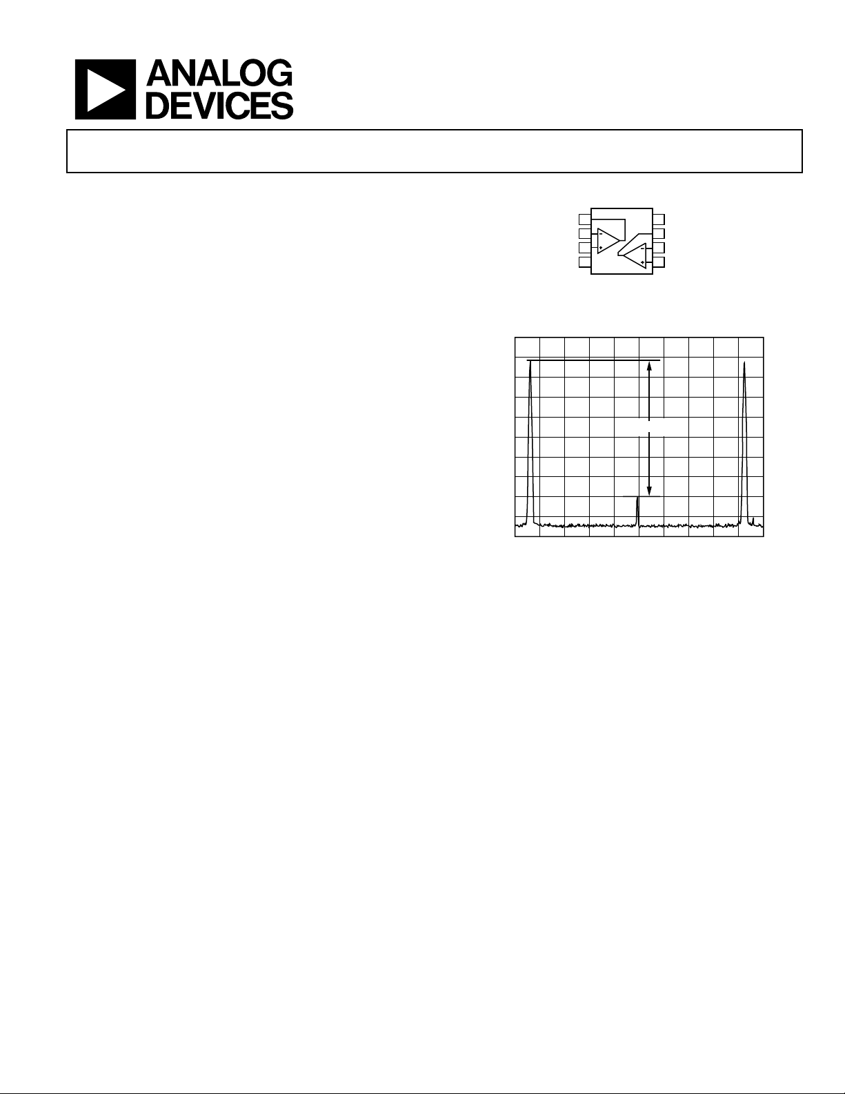
Figure 2. AD45048AR Upstream ADSL MTPR (13 dBm, CF = 5.3)
–68dB
+V
8
S
OUT2
7
6
–IN2
5
+IN2
AD45048
04817-Sp0-001
04817-Sp0-002
GENERAL DESCRIPTION
The AD45048 ADSL CPE line driver is a dual operational
amplifier capable of driving high output current (230 mA) and
features a rail-to-rail output stage that swings to within 0.5 V of
the supply rails. The AD45048 rail-to-rail output stage surpasses
the output voltage capability of typical emitter-follower output
stages and can deliver up to 23 V p-p differentially from a single
12 V supply in ADSL CPE line driving applications. The low
distortion, high output current, and wide output dynamic range
make the AD45048 ideal for driving upstream signals in ADSL
CPE applications.
Fabricated with ADI’s high speed XFCB-HV (eXtra Fast
Complementary Bipolar-High Voltage) process, the high
bandwidth and fast slew rate of the AD45048 keep distortion to
a minimum while dissipating minimum power. The AD45048 is
available in a standard 8-lead SOIC package that can operate
from −40°C to +85°C.
Rev. 0
Information furnished by Analog Devices is believed to be accurate and reliable.
However, no responsibility is assumed by Analog Devices for its use, nor for any
infringements of patents or other rights of third parties that may result from its use.
Specifications subject to change without notice. No license is granted by implication
or otherwise under any patent or patent rights of Analog Devices. Trademarks and
registered trademarks are the property of their respective owners.
One Technology Way, P.O. Box 9106, Norwood, MA 02062-9106, U.S.A.
Tel: 781.329.4700
Fax: 781.326.8703 © 2004 Analog Devices, Inc. All rights reserved.
www.analog.com
Page 2

AD45048
TABLE OF CONTENTS
Specifications..................................................................................... 3
Layout Considerations..................................................................7
Absolute Maximum Ratings............................................................ 4
ESD Caution.................................................................................. 4
Typical Performance Characteristics............................................. 5
General Description......................................................................... 7
Power Supply and Decoupling.................................................... 7
REVISION HISTORY
7/04—Revision 0: Initial Version
CPE ADSL Application.................................................................7
Transformer Sel ecti on ..................................................................7
Receive Channel Considerations.................................................7
Outline Dimensions..........................................................................8
Ordering Guide .............................................................................8
Rev. 0 | Page 2 of 8
Page 3

AD45048
SPECIFICATIONS
VS = ±6 V or 12 V (@ TA = 25°C, G = +10, RL = 100 Ω, unless otherwise noted).
Table 1.
Parameter Test Conditions/Comments Min Typ Max Unit
DYNAMIC PERFORMANCE
−3 dB Bandwidth G = +1, V
0.1 dB Flatness V
Large Signal Bandwidth V
Large Signal Slew Rate V
OUT
OUT
OUT
NOISE/DISTORTION PERFORMANCE
Distortion (Worst Harmonic) fC = 40 kHz, V
Multitone Power Ratio 26 kHz to 134 kHz, Z
Input Voltage Noise f = 100 kHz 4.5 nV/√Hz
Input Current Noise f = 100 kHz 1.5 pA/√Hz
DC PERFORMANCE
Input Offset Voltage 1 2.5 mV
T
MIN
− T
Input Offset Voltage Match 1 2.0 mV
Input Bias Current 200 900 nA
T
MIN
− T
Input Offset Current 50 300 nA
Open-Loop Gain 85 94 dB
INPUT CHARACTERISTICS
Input Resistance f = 100 kHz 87 kΩ
Input Capacitance 1.4 pF
OUTPUT CHARACTERISTICS
Output Resistance 1.4 MHz; G = +1 0.2 Ω
Output Voltage Swing Maximum Swing (Differential) V
Minimum Swing (Differential) V
Differential Output Voltage Swing ∆V
Single-Ended +Swing R
Single-Ended -Swing R
Single-Ended +Swing R
Single-Ended –Swing R
OUT
LOAD
LOAD
LOAD
LOAD
Operating Range (Dual Supply) ±1.5 ±12.6 V
Supply Current 7 9 12 mA
Power Supply Rejection Ratio ±0.5 V −85 −75 dB
Common-Mode Rejection Ratio ±1 V −86 −79 dB
= 0.1 V p-p, RFB = 0 Ω, R
OUT
= 0.1 V p-p Single-Ended, G = +1, R
= 1 V p-p Single-Ended, G = +10, R
= 5 V p-p, G = +1, R
= 6 V p-p, Single-Ended, R
OUT
LINE
MAX
MAX
= V
− V
OMAX
OMIN
= 25 Ω 55 V/µs
LOAD
= 100 Ω, XFMR = 1:2 turns, P
= 25 Ω 65 MHz
LOAD
= 25 Ω 3.35 MHz
LOAD
= 25 Ω 4.5 MHz
LOAD
= 25 Ω −80 dBc
LOAD
= 13 dBm −68 dBc
LINE
2.5 mV
1.3 µA
, R
OMAX
OMIN
= 50 Ω Differential +11.25 +11.5 V diff
LOAD
, R
= 50 Ω Differential −11.5 −11.25 V diff
LOAD
22.5 23 V p-p
= 25 Ω +5.68 +5.76 Vp
= 25 Ω −5.67 −5.58 V
= 100 Ω +5.92 +5.95 V
= 100 Ω −5.91 −5.86 V
p
p
p
Rev. 0 | Page 3 of 8
Page 4

AD45048
ABSOLUTE MAXIMUM RATINGS
Table 2.
Parameter Rating
Supply Voltage 26.4 V
Power Dissipation (T
Storage Temperature −65°C to +125°C
Operating Temperature Range −40°C to +85°C
Lead Temperature Range
(Soldering 10 sec)
Junction Temperature 150°C
JMAX
300°C
– TA)/θ
1
JA
ESD CAUTION
ESD (electrostatic discharge) sensitive device. Electrostatic charges as high as 4000 V readily accumulate
on the human body and test equipment and can discharge without detection. Although this product features
proprietary ESD protection circuitry, permanent damage may occur on devices subjected to high energy electrostatic discharges. Therefore, proper ESD precautions are recommended to avoid performance degradation
or loss of functionality.
Stresses above those listed under Absolute Maximum Ratings
may cause permanent damage to the device. This is a stress
rating only; functional operation of the device at these or any
other conditions above those indicated in the operational
section of this specification is not implied. Exposure to absolute
maximum rating conditions for extended periods may affect
device reliability.
1
θJA = 112.7°C/W for SOIC package in still air based on 2S2P JEDEC PCB.
Rev. 0 | Page 4 of 8
Page 5

AD45048
TYPICAL PERFORMANCE CHARACTERISTICS
25
G = +10
20
G = +5
15
10
G = +2
5
G = +1
0
GAIN (dB)
–5
–10
–15
–20
–25
10k 100k 1M 10M 1G100M
FREQUENCY (Hz)
R
G
Figure 3. Noninverting Small Signal Bandwidth
= ±6 V, VO = 0.1 V p-p, RL = 25 Ω)
(V
S
25
G = –10
20
G = –5
15
10
G = –2
5
G = –1
0
GAIN (dB)
–5
–10
–15
–20
–25
10k 100k 1M 10M 100M 1G
FREQUENCY (Hz)
R
G
Figure 4. Inverting Small Signal Bandwidth
= ±6 V, VO = 0.1 V p-p, RL = 25 Ω)
(V
S
–40
–50
–60
MTPR
–70
–80
0 5 10 15 20
dBm (100Ω)
Figure 5. MTPR vs. Line Power (See Schematic in Figure 8)
499Ω
–
+
5kΩ
–
+
25Ω
04817-Sp0-017
25Ω
04817-Sp0-025
04817-Sp0-027
25
G = +10
20
G = +5
15
10
G = +2
5
G = +1
0
GAIN (dB)
–5
–10
–15
–20
–25
10k 100k 1M 10M 100M 1G
FREQUENCY (Hz)
R
G
Figure 6. Noninverting Large Signal Bandwidth
= ±6 V, VO = 1 V p-p, RL = 25 Ω)
(V
S
25
G = –10
20
G = –5
15
10
G = –2
5
G = –1
0
GAIN (dB)
–5
–10
–15
–20
–25
10k 100k 1M 10M 100M 1G
FREQUENCY (Hz)
R
G
Figure 7. Inverting Large Signal Bandwidth
= ±6 V, VO = 1 V p-p, RL = 25 Ω)
(V
S
R2
3kΩ
+12V
R5
3kΩ
4.7µF
TANT
R3
1
7
12.5Ω
R6
12.5Ω
R1
499Ω
+V
IN
+6V
R4
499Ω
–V
IN
0.1µF
8
2
V+
OUT
3
5
6
AD45048
OUT
V–
AD45048
4
U1A
U1B
Figure 8. Differential Test Circuit for MTPR
499Ω
–
+
5kΩ
–
+
TX1
1:2
25Ω
25Ω
R3
100Ω
04817-Sp0-026
04817-Sp0-018
04817-Sp0-014
Rev. 0 | Page 5 of 8
Page 6

AD45048
100
100
10
VOLTAGE NOISE (nV/ Hz)
1
10 100 1k 10k 100k 1M 10M 100M
Figure 9. Voltage Noise vs. Frequency, V
0
–20
–40
–60
–80
DISTORTION (dBc)
–100
–120
13579246810
Figure 10. Single-Ended Harmonic Distortion, V
R
= 499 Ω, RG = 100 Ω, RL = 25 Ω, Fundamental Frequency = 40 kHz
F
FREQUENCY (Hz)
SECOND
THIRD
OUTPUT VOLTAGE (p-p)
= ±6 V
S
= ±6 V dc, G = +6,
S
04817-Sp0-019
04817-Sp0-028
11
10
CURRENT NOISE (pA/ Hz)
1
10 100 1k 10k 100k 1M 10M
Figure 12. Input Current Noise vs. Frequency, V
1000
100
10
1
0.1
OUTPUT IMDEDANCE (Ω)
0.01
0.001
10k 100k 1M 10M 100M
FREQUENCY (Hz)
FREQUENCY (Hz)
= ±6 V
S
Figure 13. Output Impedance vs. Frequency
04817-Sp0-020
04817-Sp0-030
2V/DIV
M 5.00µs
Figure 11. Discrete Multitone Modulation Overdrive Recovery
(See Schematic in Figure 8)
04817-Sp0-029
Rev. 0 | Page 6 of 8
50mV/DIV
M 100ns
Figure 14. Small Signal Pulse Response R
= 1 kΩ, RFB = 500 Ω
LOAD
04817-Sp0-031
Page 7

AD45048
GENERAL DESCRIPTION
The AD45048 is a voltage feedback, rail-to-rail output amplifier
with high output current capability. Fabricated on Analog
Devices’ proprietary high speed, eXtra Fast Complementary
Bipolar High Voltage process (XFCB-HV), the high bandwidth
and fast slew rate of the AD45048 keep distortion to a minimum while dissipating minimum power. The XFCB-HV, Silicon
on Insulator (SOI) process prevents latch-up problems and enables the construction of high frequency, low distortion
amplifiers, such as the AD45048.
POWER SUPPLY AND DECOUPLING
The AD45048 can be powered with a good quality, well
regulated, low noise supply anywhere in the range from +3 V to
±12.6 V. In order to optimize the AD45048 in standard ADSL
CPE line driver applications (see Figure 8), power the amplifier
with a well regulated 12 V supply. Careful attention should be
paid to decoupling the power supply. High quality capacitors
with low equivalent series resistance (ESR), such as multilayer
ceramic capacitors (MLCCs), should be used to minimize the
supply voltage ripple and power dissipation. A 0.1 µF MLCC
decoupling capacitor(s) should be located no more than
1/8-inch away from the power supply pin(s). A large, usually
tantalum, 10 µF to 47 µF capacitor is recommended to provide
good decoupling for lower frequency signals and to supply
current for fast, large signal changes at the AD45048 outputs.
LAYOUT CONSIDERATIONS
As is the case with all high speed applications, careful attention
to printed circuit board layout details prevent associated board
parasitics from becoming problematic. Proper RF layout and
printed circuit board design techniques are strongly recommended. The PCB should have a low impedance return path (or
ground) to the supply. Removing the ground plane from all
layers in the immediate area of the amplifier reduces stray
capacitances. The signal routing should be short and direct in
order to minimize the parasitic inductance and capacitance
associated with these traces. Termination resistors and loads
should be located as close as possible to their respective inputs
and outputs. Input traces should be kept as far apart as possible
from the output traces to minimize coupling (crosstalk) though
the board.
Wherever there are complementary signals, a symmetrical
layout should be provided to the extent possible in order to
maximize balanced performance. When running differential
signals over a long distance, the traces on the PCB should be
close together or any differential wiring should be twisted
together to minimize the area of the loop that is formed. This
reduces the radiated energy and makes the circuit less
susceptible to RF interference. Adherence to stripline design
techniques for long signal traces (greater than about 1 inch) is
recommended.
CPE ADSL APPLICATION
The low cost, high output current dual AD45048 xDSL line
driver amplifiers have been specifically designed to drive high
fidelity xDSL signals to within 0.5 V of the power rails on a
single 12 V supply. The AD45048 may be used in transformercoupled bridge hybrid circuits designed to drive modulated
signals, including discrete multitone (DMT), upstream to the
central office.
TRANSFORMER SELECTION
Customer premise ADSL applications require the transmission
of a 13 dBm DMT signal (20 mW into 100 Ω). DMT signals can
have a crest factor (V peak/V rms ratio) as high as 5.3, requiring
the line driver to provide peak power of 560 mW. The line
driver is required to drive a 7.5 V peak onto the 100 Ω telephone line while maintaining about −65 dBc to −70 dBc of
MTPR. Since the maximum, low distortion output swing available from the AD45048 line driver is approximately 11.5 V on a
12 V supply (depending on the load), and taking into account
the power lost in the transformer and termination resistors, a
step-up transformer with a minimum turns ratio of 1.5 or
greater is needed. In the simplified differential driver circuit
shown in Figure 8, the AD45048 is driving a 25 Ω impedance
reflected by 1:2 step-up transformer. R3 and R6 are 12.5 Ω each
and are back-termination or load-matching resistors whose
values can be calculated by
2
(100 Ω/(N
where 100 Ω is the approximate phone line impedance and N is
the transformer turns ratio. In Figure 8, the total differential
load including the termination resistors is 50 Ω, and under
these conditions, the AD45048 is capable of driving low
distortion signals to within 0.5 V of the power rails.
))/2
RECEIVE CHANNEL CONSIDERATIONS
A step-up transformer of N turns used at the output of the
differential line driver increases the differential output voltage
to the line (see Figure 8). However, the inverse effect is seen in
the receive channel as the amplitude of signal on the driver side
of the transformer is divided by N turns. The decision to use a
particular transformer turns ratio may be impacted by the
ability of the receive circuitry to resolve low level signals in the
noisy twisted pair telephone plant. Higher turns ratio transformers reduce the effective receive channel SNR (signal-tonoise ratio) due to the reduction in the received signal strength.
An amplifier with low RTI noise, such as the AD8022
(2.5 nV/√Hz), is recommended for the receive channel. For a
complete selection of amplifiers and other related components,
www.analog.com.
see
Rev. 0 | Page 7 of 8
Page 8

AD45048
Y
OUTLINE DIMENSIONS
4.00 (0.1574)
3.80 (0.1497)
5.00 (0.1968)
4.80 (0.1890)
85
6.20 (0.2440)
5.80 (0.2284)
41
1.27 (0.0500)
BSC
0.25 (0.0098)
0.10 (0.0040)
COPLANARIT
0.10
CONTROLLING DIMENSIONS ARE IN MILLIMETERS; INCH DIMENSIONS
(IN PARENTHESES) ARE ROUNDED-OFF MILLIMETER EQUIVALENTS FOR
REFERENCE ONLY AND ARE NOT APPROPRIATE FOR USE IN DESIGN
SEATING
PLANE
COMPLIANT TO JEDEC STANDARDS MS-012AA
1.75 (0.0688)
1.35 (0.0532)
0.51 (0.0201)
0.31 (0.0122)
0.25 (0.0098)
0.17 (0.0067)
0.50 (0.0196)
0.25 (0.0099)
8°
1.27 (0.0500)
0°
0.40 (0.0157)
× 45°
Figure 15. 8-Lead Standard Small Outline Package [SOIC]
Narrow Body (R-8)
Dimensions shown in millimeters and (inches)
ORDERING GUIDE
Model Temperature Range Package Description Package Option
AD45048AR −40°C to +85°C 8-Lead Standard Small Outline Package (SOIC) R-8
AD45048AR-REEL −40°C to +85°C 8-Lead Standard Small Outline Package (SOIC) R-8
AD45048AR-REEL7 −40°C to +85°C 8-Lead Standard Small Outline Package (SOIC) R-8
© 2004 Analog Devices, Inc. All rights reserved. Trademarks and registered trademarks are the property of their respective owners.
D04817–0–7/04(0)
Rev. 0 | Page 8 of 8
 Loading...