

Page 1
Serial Input 16-Bit
V
FEATURES
4 mA–20 mA, 0 mA–20 mA or 0 mA–24 mA
current output
16-bit resolution and monotonicity
±0.012% max integral nonlinearity
±0.05% max offset (trimmable)
±0.15% max total output error (trimmable)
Flexible serial digital interface (3.3 MBPS)
On-Chip loop fault detection
On-chip 5 V reference (25 ppm/°C max)
Asynchronous CLEAR function
Maximum power supply range of 32 V
Output loop compliance of 0 V to V
24-Lead SOIC and PDIP packages
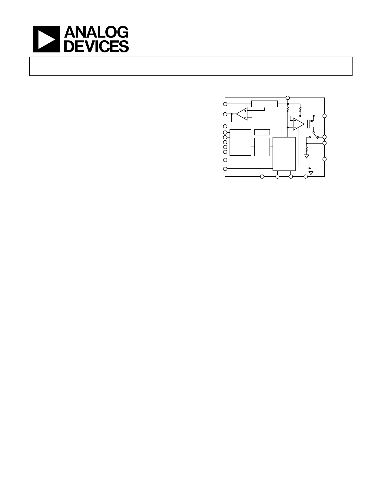
GENERAL DESCRIPTION
The AD420 is a complete digital to current loop output
converter, designed to meet the needs of the industrial control
market. It provides a high precision, fully integrated, low cost
single-chip solution for generating current loop signals in a
compact 24-lead SOIC or PDIP package.
The output current range can be programmed to 4 mA to
20 mA, 0 mA to 20 mA or to an overrange function of 0 mA to
24 mA. The AD420 can alternatively provide a voltage output from
a separate pin that can be configured to provide 0 V to 5 V, 0 V
to 10 V, ±5 V, or ±10 V with the addition of a single external
buffer amplifier.
The 3.3 M Baud serial input logic design minimizes the cost of
galvanic isolation and allows for simple connection to commonly
used microprocessors. It can be used in 3-wire or asynchronous
mode and a serial-out pin is provided to allow daisy chaining of
multiple DACs on the current loop side of the isolation barrier.
The AD420 uses sigma-delta (Σ-Δ) DAC technology to achieve
16-bit monotonicity at very low cost. Full-scale settling to 0.1%
occurs within 3 ms. The only external components that are
required (in addition to normal transient protection circuitry)
are two low cost capacitors which are used in the DAC output filter.
If the AD420 is used at extreme temperatures and supply
voltages, an external output transistor can be used to minimize
power dissipation on the chip via the BOOST pin. The FAULT
DETECT pin signals when an open circuit occurs in the loop.
The on-chip voltage reference can be used to supply a precision
+5 V to external components in addition to the AD420 or, if the
Rev. H
Information furnished by Analog Devices is believed to be accurate and reliable. However, no
responsibility is assumed by Anal og Devices for its use, nor for any infringements of patents or ot her
rights of third parties that may result from its use. Specifications subject to change without notice. No
license is granted by implication or otherwise under any patent or patent rights of Analog Devices.
Trademarks and registered trademarks are the property of their respective owners.
− 2.75 V
CC
4 mA–20 mA, 0 mA–20 mA DAC
AD420
FUNCTIONAL BLOCK DIAGRAM
CC
V
LL
REF OUT
REF IN
DATA OUT
CLEAR
LATCH
CLOCK
DATA IN
RANGE
SELECT 1
RANGE
SELECT 2
DATA I/P
REGISTER
user desires temperature stability exceeding 25 ppm/°C, an
external precision reference such as the AD586 can be used as
the reference. The AD420 is available in a 24-lead SOIC and
PDIP over the industrial temperature range of −40°C to +85°C.
PRODUCT HIGHLIGHTS
1. The AD420 is a single chip solution for generating 4 mA to
20 mA or 0 mA to 20 mA signals at the controller end of
the current loop.
2. The AD420 is specified with a power supply range from
12 V to 32 V. Output loop compliance is 0 V to V
3. The flexible serial input can be used in 3-wire mode
with SPI® or MICROWIRE® microcontrollers, or in
asynchronous mode, which minimizes the number of
control signals required.
4. The serial data out pin can be used to daisy chain any
number of AD420s together in 3-wire mode.
5. At power-up, the AD420 initializes its output to the low
end of the selected range.
6. The AD420 has an asynchronous CLEAR pin, which sends
the output to the low end of the selected range (0 mA, 4 mA,
or 0 V).
7. The AD420 BOOST pin accommodates an external
transistor to off-load power dissipation from the chip.
8. The offset of ±0.05% and total output error of ±0.15% can
be trimmed if desired, using two external potentiometers.
One Technology Way, P.O. Box 9106, Norwood, MA 02062-9106, U.S.A.
Tel: 781.329.4700 www.analog.com
Fax: 781.461.3113 ©1999–2011 Analog Devices, Inc. All rights reserved.
REFERENCE
AD420
CLOCK
16-BIT
DAC
OFFSET
TRIM
Figure 1.
4kΩ
SWITCHED
CURRENT
SOURCES
AND
FILTERING
CAP 1 CAP 2 GND
40Ω
1.25kΩ
− 2.75 V.
CC
BOOST
I
OUT
V
OUT
FAULT
DETECT
00494-001
Page 2

AD420
TABLE OF CONTENTS
Features.............................................................................................. 1
Functional Block Diagram .............................................................. 1
General Description ......................................................................... 1
Product Highlights ........................................................................... 1
Revision History ............................................................................... 2
Specifications..................................................................................... 3
Absolute Maximum Ratings............................................................ 5
ESD Caution.................................................................................. 5
Pin Configuration and Function Descriptions............................. 6
Timing Requirements ...................................................................... 7
Three-Wire Interface ................................................................... 7
Three-Wire Interface Fast Edges on Digital Input................... 7
Asynchronous Interface............................................................... 7
Terminology ...................................................................................... 8
Theory of Operation ........................................................................ 9
Applications Information .............................................................. 10
Current Output........................................................................... 10
Driving Inductive Loads............................................................ 10
Voltage-Mode Output................................................................ 10
Optional Span and Zero Trim .................................................. 10
Three-Wire Interface ................................................................. 11
Using Multiple DACS with Fault Detect ................................. 11
Asynchronous Interface Using Optocouplers ........................ 11
Microprocessor Interface............................................................... 12
AD420-To-MC68HC11 (SPI Bus) Interface........................... 12
AD420 to Microwire Interface ................................................. 12
External Boost Function ........................................................... 13
AD420 Protection........................................................................... 14
Transient Voltage Protection .................................................... 14
Board Layout And Grounding ................................................. 14
Power Supplies and Decoupling............................................... 14
Outline Dimensions....................................................................... 15
Ordering Guide .......................................................................... 15
REVISION HISTORY
1/11—Rev. G to Rev. H
Changes to Figure 13...................................................................... 13
Changes to Ordering Guide.......................................................... 15
11/09—Rev. F to Rev. G
Updated Format..................................................................Universal
Changes to Table 2............................................................................ 5
Updated Outline Dimensions....................................................... 15
Changes to Ordering Guide.......................................................... 15
9/99—Rev. E to Rev. F
Rev. H | Page 2 of 16
Page 3

AD420
SPECIFICATIONS
TA = T
Table 1.
AD420-32 Version
Parameter Min Typ Max Units Comments
RESOLUTION 16 Bits
I
OUT
V
OUT
VOLTAGE REFERENCE
DIGITAL INPUTS
DIGITAL OUTPUTS
− T
MIN
CHARACTERISTICS RL = 500 Ω
Operating Current Ranges 4 20 mA
0 20 mA
0 24 mA
Current Loop Voltage Compliance 0 VCC − 2.75 V V
Settling Time (to 0.1% of FS)1 2.5 3 ms
Output Impedance (Current Mode) 25 MΩ
Accuracy2
Monotonicity 16 Bits
Integral Nonlinearity ±0.002 ±0.012 %
Offset (0 mA or 4 mA) (TA = +25°C) ±0.05 %
Offset Drift 20 50 ppm/° C
Total Output Error (20 mA or 24 mA) (TA = +25°C) ±0.15 %
Total Output Error Drift 20 50 ppm/° C
PSRR3 5 10 μA/V
CHARACTERISTICS
FS Output Voltage Range (Pin 17) 0 5 V
REF OUT
Output Voltage (TA = +25° C) 4.995 5.0 5.005 V
Drift ±25 ppm/° C
Externally Available Current 5 mA
Short Circuit Current 7 mA
REF IN
Resistance 30 kΩ
VLL
Output Voltage 4.5 V
Externally Available Current 5 mA
Short Circuit Current 20 mA
VIH (Logic 1) 2.4 V
VIL (Logic 0) 0.8 V
IIH (VIN = 5.0 V) ±10 μA
IIL (VIN = 0 V) ±10 μA
Data Input Rate (3-Wire Mode) No Minimum 3.3 MBPS
Data Input Rate (Asynchronous Mode) No Minimum 150 kBPS
FAU LT D EFEC T
VOH (10 kΩ Pull-Up Resistor to VLL) 3.6 4.5 V
VOL (10 kΩ Pull-Up Resistor to VLL) 0.2 0.4 V
VOL @ 2.5 mA 0.6 V
DATA OUT
VOH (IOH = −0.8 mA) 3.6 4.3 V
VOL (IOL = 1.6 mA) 0.3 0.4 V
, VCC = +24 V, unless otherwise noted.
MAX
Rev. H | Page 3 of 16
Page 4

AD420
AD420-32 Version
Parameter Min Typ Max Units Comments
POWER SUPPLY
Operating Range VCC 12 32 V
Quiescent Current 4.2 5.5 mA
Quiescent Current (External VLL) 3 mA
TEMPERATURE RANGE
Specified Performance −40 +85 °C
1
External capacitor selection must be as described in Figure 6.
2
Total Output Error includes Offset and Gain Error. Total Output Error and Offset Error are with respect to the Full-Scale Output and are measured with an ideal +5 V
reference. If the internal reference is used, the reference errors must be added to the Offset and Total Output Errors.
3
PSRR is measured by varying VCC from 12 V to its maximum 32 V.
Rev. H | Page 4 of 16
Page 5
AD420
ABSOLUTE MAXIMUM RATINGS
Table 2.
Parameter Rating
VCC to GND 32 V
I
to GND VCC
OUT
Digital Inputs to GND −0.5 V to +7 V
Digital Output to GND −0.5 V to VLL + 0.3 V
VLL and REF OUT: Outputs Safe for
Indefinite Short to Ground
Storage Temperature −65°C to +150°C
Lead Temperature (Soldering, 10 sec) +300°C
Lead Temperature, Soldering Reflow +260°C
Thermal Impedance:
SOIC (R) Package θJA = 75°C/W
PDIP (N) Package θJA = 50°C/W
Stresses above those listed under Absolute Maximum Ratings
may cause permanent damage to the device. This is a stress
rating only; functional operation of the device at these or any
other conditions above those indicated in the operational
section of this specification is not implied. Exposure to absolute
maximum rating conditions for extended periods may affect
device reliability.
Table 3. Truth Table
Inputs
Range
CLEAR
0 X X Normal operation
1 X X
X 0 0 0 V–5 V range
X 0 1 4 mA–20 mA range
X 1 0 0 mA–20 mA range
X 1 1 0 mA–24 mA range
Select 2
Range
Select 1 Operation
Output at bottom of
span
ESD CAUTION
Rev. H | Page 5 of 16
Page 6

AD420
PIN CONFIGURATION AND FUNCTION DESCRIPTIONS
1
NC
V
2
LL
CLEAR
LATCH
CLOCK
DATA IN
GND
NC
3
4
AD420
5
TOP VIEW
6
(Not to Scale)
7
8
9
10
11
12
NC = NO CONNECT
FAULT DETECT
RANGE SELECT 2
RANGE SELECT 1
DATA OUT
Figure 2. Pin Configuration
Table 4. Pin Function Descriptions
Pin No. Mnemonic Function
1, 12,
NC No Connection. No internal connections inside device.
13, 24
2 VLL
Auxiliary buffered +4.5 V digital logic voltage. This pin is the internal supply voltage for the digital
circuitry and can be used as a termination for pull-up resistors. An external +5 V power supply can be
connected to V
pin should be decoupled to GND with a 0.1 μF capacitor. See the Power Supplies and Decoupling
V
LL
. It will override this buffered voltage, thus reducing the internal power dissipation. The
LL
section.
3 FAULT DETECT
FAULT DETECT, connected to a pull-up resistor, is asserted low when the output current does not match
the DAC’s programmed value, for example, in case the current loop is broken.
4 RANGE SELECT 2 Selects the converter’s output operating range. One output voltage range and three
5 RANGE SELECT 1 output current ranges are available.
6 CLEAR
unconditionally forces the output to go to the minimum of its programmed range. After CLEAR
Valid V
IH
is removed the DAC output will remain at this value. The data in the input register is unaffected.
7 LATCH
In the 3-wire interface mode a rising edge parallel loads the serial input register data into the DAC. To
use the asynchronous mode connect LATCH through a current limiting resistor to V
8 CLOCK
Data Clock Input. The clock period is equal to the input data bit rate in the 3-wire interface mode and is
16 times the bit rate in asynchronous mode.
9 DATA IN Serial Data Input.
10 DATA OUT
Serial Data Output. In the 3-wire interface mode, this output can be used for daisy-chaining multiple
AD420s. In the asynchronous mode a positive pulse will indicate a framing error after the stop-bit is
received.
11 GND Ground (Common).
14 REF OUT +5 V Reference Output.
15 REF IN Reference Input.
16 OFFSET TRIM Offset Adjust.
17 V
18 I
19 BOOST
Voltage Output.
OUT
Current Output.
OUT
Connect to an external transistor to reduce the power dissipated in the AD420 output transistor, if
desired.
20 CAP 1 These pins are used for internal filtering. Connect capacitors between each of these
21 CAP 2 pins and VCC. Refer to the description of current output operation.
22 NC No Connection. Do not connect anything to this pin.
23 VCC
Power Supply Input. The V
pin should always be decoupled to GND with a 0.1 μF capacitor. See the
CC
Power Supplies and Decoupling section.
24
NC
V
23
CC
22
NC
CAP 2
21
CAP 1
20
BOOST
19
I
18
OUT
V
17
OUT
OFFSET TRIM
16
15
REF IN
REF OUT
14
13
NC
00494-002
.
CC
Rev. H | Page 6 of 16
Page 7

AD420
TIMING REQUIREMENTS
TA = −40°C to +85°C, VCC = +12 V to +32 V.
THREE-WIRE INTERFACE
CLOCK
WORD “N” WORD “N + 1”
DATA IN
LATCH
DATA OUT
CLOCK
DATA IN
LATCH
DATA OUT
1011001 1 100 111110 0 00
B8
B15
(MSB)
B11
B14
B13
B12
B10
WORD “N – 1” WORD “N”
t
CK
t
CL
t
CH
t
t
DH
DS
t
DW
B7
B9
B3B2B1
B5B4B6
t
LD
t
LL
t
SD
B0
B15
(LSB)
1101
B14
B15
t
LH
B14
B13
B12
B13
B12
Figure 3. Timing Diagram for 3-Wire Interface
Table 5. Timing Specification for 3-Wire Interface
Parameter Label Limit Units
Data Clock Period t
300 ns min
CK
Data Clock Low Time tCL 80 ns min
Data Clock High Time tCH 80 ns min
Data Stable Width tDW 125 ns min
Data Setup Time t
Data Hold Time t
Latch Delay Time t
Latch Low Time t
Latch High Time t
40 ns min
DS
5 ns min
DH
80 ns min
LD
80 ns min
LL
80 ns min
LH
Serial Output Delay Time tSD 225 ns max
Clear Pulse Width t
50 ns min
CLR
THREE-WIRE INTERFACE FAST EDGES ON DIGITAL INPUT
With a fast rising edge (<10 ns) on one of the serial inputs
(CLOCK, DATA IN, LATCH) while another input is logic high,
the part may be triggered into a test mode and the contents of
the data register may become corrupted, which may result in
the output being loaded with an incorrect value. If fast edges are
expected on the digital input lines, it is recommended that the
latch line remain at Logic 0 during serial loading of the DAC.
Similarly, the clock line should remain low during updates of
the DAC via the latch pin. Alternatively, the addition of small
value capacitors on the digital lines will slow down the edge.
00494-003
CLOCK
DATA IN
(INTERNALLY GENERATED LATCH)
CLOCK
DATA IN
CLOCK
DATA IN
01
BIT
START
EXPANDED TIME VIEW BELOW
CLOCK COUNTER ST ARTS HERE
012 8 16 24
START BIT
001
BIT14
t
ACH
t
ADH
BIT13
DATA BIT 15
BIT15
CONFIRM START BIT
EXPANDED TIME VIEW BELOW
t
ACK
t
ACL
t
ADS
t
ADW
BIT0
TO BIT1
SAMPLE BIT 15
STOP
BIT
BIT 14
NEXT
BIT
START
Figure 4. Timing Diagram for Asynchronous Interface
Table 6. Timing Specifications for Asynchronous Interface
Parameter Label Limit Units
Asynchronous Clock Period t
Asynchronous Clock Low Time t
Asynchronous Clock High Time t
Data Stable Width (Critical Clock Edge) t
Data Setup Time (Critical Clock Edge) t
Data Hold Time (Critical Clock Edge) t
Clear Pulse Width t
400 ns min
ACK
50 ns min
ACL
150 ns min
ACH
300 ns min
ADW
60 ns min
ADS
20 ns min
ADH
50 ns min
CLR
ASYNCHRONOUS INTERFACE
Note that in the timing diagram for asynchronous mode operation each data word is framed by a START (0) bit and a STOP
(1) bit. The data timing is with respect to the rising edge of the
CLOCK at the center of each bit cell. Bit cells are 16 clocks
long, and the first cell (the START bit) begins at the first clock
following the leading (falling) edge of the START bit. Thus, the
MSB (D15) is sampled 24 clock cycles after the beginning of
the START bit, D14 is sampled at clock number 40, and so on.
During any dead time before writing the next word the DATA
IN pin must remain at Logic 1.
The DAC output updates when the STOP bit is received. In
the case of a framing error (the STOP bit sampled as a 0) the
AD420 will output a pulse at the DATA OUT pin one clock
period wide during the clock period subsequent to sampling
the STOP bit. The DAC output will not update if a framing
error is detected.
00494-004
Rev. H | Page 7 of 16
Page 8

AD420
TERMINOLOGY
Resolution
For 16-bit resolution, 1 LSB = 0.0015% of the FSR. In the
4 mA–20 mA range 1 LSB = 244 nA.
Integral Nonlinearity
Analog Devices defines integral nonlinearity as the maximum
deviation of the actual, adjusted DAC output from the ideal
analog output (a straight line drawn from 0 to FS – 1 LSB) for
any bit combination. This is also referred to as relative accuracy.
Differential Nonlinearity
Differential nonlinearity is the measure of the change in the
analog output, normalized to full scale, associated with an LSB
change in the digital input code. Monotonic behavior requires
that the differential linearity error be greater than –1 LSB over
the temperature range of interest.
Monotonicity
A DAC is monotonic if the output either increases or remains
constant for increasing digital inputs with the result that the
output will always be a single-valued function of the input.
Gain Error
Gain error is a measure of the output error between an ideal
DAC and the actual device output with all 1s loaded after offset
error has been adjusted out.
Offset Error
Offset error is the deviation of the output current from its ideal
value expressed as a percentage of the fullscale output with all
0s loaded in the DAC.
Drift
Drift is the change in a parameter (such as gain and offset) over
a specified temperature range. The drift temperature coefficient,
specified in ppm/°C, is calculated by measuring the parameter
at T
, 25°C, and T
MIN
and dividing the change in the
MAX
parameter by the corresponding temperature change.
Current Loop Voltage Compliance
The voltage compliance is the maximum voltage at the I
OUT
pin for
which the output current will be equal to the programmed value.
Rev. H | Page 8 of 16
Page 9

AD420
V
THEORY OF OPERATION
The AD420 uses a sigma-delta (Σ-Δ) architecture to carry out
the digital-to-analog conversion. This architecture is particularly
well suited for the relatively low bandwidth requirements of the
industrial control environment because of its inherent
monotonicity at high resolution.
In the AD420 a second order modulator is used to keep complexity and die size to a minimum. The single bit stream from
the modulator controls a switched current source that is then
filtered by two, continuous time resistor-capacitor sections.
The capacitors are the only external components that have to be
added for standard current-out operation. The filtered current
is amplified and mirrored to the supply rail so that the application
simply sees a 4 mA–20 mA, 0 mA–20 mA, or 0 mA–24 mA
current source output with respect to ground. The AD420
is manufactured on a BiCMOS process that is well suited to
implementing low voltage digital logic with high performance
and high voltage analog circuitry.
The AD420 can also provide a voltage output instead of a current
loop output if desired. The addition of a single external amplifier
allows the user to obtain 0 V–5 V, 0 V–10 V, ±5 V, or ±10 V.
The AD420 has a loop fault detection circuit that warns if the
voltage at I
attempts to rise above the compliance range, due
OUT
to an open-loop circuit or insufficient power supply voltage. The
FAULT DETECT is an active low open drain signal so that one
can connect several AD420s together to one pull-up resistor for
global error detection. The pull-up resistor can be tied to the
V
pin, or an external +5 V logic supply.
LL
The I
current is controlled by a PMOS transistor and an
OUT
internal amplifier as shown in the functional block diagram.
The internal circuitry that develops the fault output avoids
using a comparator with window limits since this would require
an actual output error before the FAULT DETECT output
becomes active. Instead, the signal is generated when the
internal amplifier in the output stage of the AD420 has less than
approximately one volt remaining of drive capability (when
the gate of the output PMOS transistor nearly reaches ground).
Thus the FAULT DETECT output activates slightly before the
compliance limit is reached. Since the comparison is made
within the feedback loop of the output amplifier, the output
accuracy is maintained by its open-loop gain, and no output
error occurs before the fault detect output becomes active.
The 3-wire digital interface, comprising DATA IN, CLOCK,
and LATCH, interfaces to all commonly used serial microprocessors without the addition of any external glue logic. Data is
loaded into an input register under control of CLOCK and is
loaded to the DAC when LATCH is strobed. If a user wants to
minimize the number of galvanic isolators in an intrinsically
safe application, the AD420 can be configured to run in
asynchronous mode. This mode is selected by connecting the
LATCH pin to V
through a current limiting resistor. The data
CC
must then be combined with a start and stop bit to frame the
information and trigger the internal LATCH signal.
CC
V
REF OUT
REF IN
DATA OUT
CLEAR
LATCH
CLOCK
DATA IN
RANGE
SELECT 1
RANGE
SELECT 2
2
LL
14
15
10
6
DATA I/P
7
REGISTER
8
9
5
4
REFERENCE
AD420
CLOCK
16-BIT
DAC
OFFSET
TRIM
23
4kΩ
SWITCHED
CURRENT
SOURCES
AND
FILTERING
CAP 1 CAP 2 GND
40Ω
21 112016
1.25kΩ
19
18
17
3
BOOST
I
OUT
V
OUT
FAULT
DETECT
Figure 5. Functional Block Diagram
00494-005
Rev. H | Page 9 of 16
Page 10

AD420
V
V
V
APPLICATIONS INFORMATION
CURRENT OUTPUT
The AD420 can provide 4 mA–20 mA, 0 mA–20 mA, or 0 mA–
24 mA output without any active external components. Filter
capacitors C1 and C2 can be any type of low cost ceramic
capacitors. To meet the specified full-scale settling time of 3 ms,
low dielectric absorption capacitors (NPO) are required.
Suitable values are C1 = 0.01 μF and C2 = 0.01 μF.
CC
0.1µF0. 1µF
GND
I
(4mA TO 20mA)
OUT
R
LOAD
00494-006
RANGE
SELECT 1
RANGE
SELECT 2
CLEAR
LATCH
CLOCK
DATA IN
V
LL
C1 C2
2 20
5
4
6 18
7
8
9
14 15 11
21 23
AD420
REF INREF OUT
Figure 6. Standard Configuration
DRIVING INDUCTIVE LOADS
When driving inductive or poorly defined loads ,connect a 0.01 μF
capacitor between I
(Pin 18) and GND (Pin 11). This ensures
OUT
stability of the AD420 with loads beyond 50 mH. There is no
maximum capacitance limit. The capacitive component of the
load may cause slower settling, though this may be masked by
the settling time of the AD420. A programmed change in the
current may cause a back EMF voltage on the output that may
exceed the compliance of the AD420. To prevent this voltage
from exceeding the supply rails connect protective diodes
between I
and each of VCC and GND.
OUT
VOLTAGE-MODE OUTPUT
Since the AD420 is a single supply device, it is necessary to add
an external buffer amplifier to the V
of bipolar output voltage ranges as shown in Figure 7.
V
LL
0.1µF
RANGE
SELECT 1
RANGE
SELECT 2
CLEAR
LATCH
CLOCK
DATA IN
C1 C2
2 20
5
4
6 17
7
8
9
14 15 11
21 23
AD420
REF INREF OUT
Figure 7.
pin to obtain a selection
OUT
CC
0.1µF
V
OUT
R3
R2
R1
GND
V
OUT
00494-007
Table 7. Buffer Amplifier Configuration
R1 R2 R3 V
OUT
Open Open 0 0 V − 5 V
Open R R
R Open R ±5 V
R 2R 2R ±10 V
Suitable R = 5 kΩ.
OPTIONAL SPAN AND ZERO TRIM
For users who would like lower than the specified values of
offset and gain error, Figure 8 shows a simple way to trim these
parameters. Care should be taken to select low drift resistors
because they affect the temperature drift performance of
the DAC.
The adjustment algorithm is iterative. The procedure for
trimming the AD420 in the 4 mA–20 mA mode can be
accomplished as follows:
1. Offset adjust. Load all zeros. Adjust RZERO for
4.00000 mA of output current.
2. Gain adjust. Load all ones. Adjust RSPAN for 19.99976 mA
(FS − 1 LSB) of output current.
Return to Step I and iterate until convergence is obtained.
GND
CC
19
I
OUT
18
5kΩ
RSPAN2
BOOST
(4mA TO 20mA)
R
LOAD
0.1µF
00494-008
V
LL
0.1µF
RANGE
SELECT 1
RANGE
SELECT 2
CLEAR
LATCH
CLOCK
DATA IN
REF OUT
C1 C2
2 20
5
4
6
7
8
9
AD420
14 15 16 11
500Ω
RSPAN
21 23
10kΩ
RZERO
Figure 8. Offset and Gain Adjust
Variation of RZERO between REF OUT (5 V) and GND leads
to an offset adjust range from −1.5 mA to 6 mA, (1.5 mA/V
centered at 1 V).
The 5 kΩ RSPAN2 resistor is connected in parallel with the
internal 40 W sense resistor, which leads to a gain increase of
+0.8%.
As RSPAN is changed to 500 Ω, the voltage on REF IN is
attenuated by the combination of RSPAN and the 30 kΩ REF IN
input resistance. When added together with RSPAN2 this
results in an adjustment range of −0.8% to +0.8%.
Rev. H | Page 10 of 16
Page 11

AD420
V
THREE-WIRE INTERFACE
Figure 9 shows the AD420 connected in the 3-wire interface
mode. The AD420 data input block contains a serial input shift
register and a parallel latch. The contents of the shift register
are controlled by the DATA IN signal and the rising edges of the
CLOCK. Upon request of the LATCH pin the DAC and internal
latch are updated from the shift register parallel outputs. The
CLOCK should remain inactive while the DAC is updated.
Refer to the timing requirements for 3-wire interface.
FAULT DETECT
LATCH
CLOCK
DATA IN
AD420
DAC1
FAU LT
DETECT
LATCH
CLOCK
DATA
IN
GND
V
CC
DATA
OUT
I
OUT
V
CC
10kΩ
R
LOAD
Figure 9. Three-Wire Interface Using Multiple DACs with Joint Fault Detect
AD420
V
LL
FAU LT
DETECT
LATCH
CLOCK
DATA
IN
GND
DAC2
V
DATA
OUT
I
OUT
V
CC
CC
R
LOAD
USING MULTIPLE DACS WITH FAULT DETECT
The 3-wire interface mode can utilize the serial DATA OUT for
easy interface to multiple DACs. To program the two AD420s in
Figure 9, 32 data bits are required. The first 16 bits are clocked
into the input shift register of DAC1. The next 16 bits
transmitted pass the first 16 bits from the DATA OUT pin of
DAC1 to the input register of DAC2. The input shift registers of
the two DACs operate as a single 32-bit shift register, with the
leading 16 bits representing information for DAC2 and the
trailing 16 bits serving for DAC1. Each DAC is then updated
upon request of the LATCH pin. The daisy-chain can be
extended to as many DACs as required.
00494-009
ASYNCHRONOUS INTERFACE USING OPTOCOUPLERS
The AD420 connected in asynchronous interface mode with
optocouplers is shown in Figure 10. Asynchronous operation
minimizes the number of control signals required for isolation
of the digital system from the control loop. The resistor connected
between the LATCH pin and V
mode. For operation with V
resistor; from 18 V to 32 V, use 100 kΩ.
Asynchronous mode requires that the clock run at 16 times the
data bit rate, therefore, to operate at the maximum input data rate
of 150 kBPS, an input clock of 2.4 MHz is required. The actual
data rate achieved may be limited by the type of optocouplers
chosen. The number of control signals can be further reduced
by creating the appropriate clock signal on the current loop
side of the isolation barrier. If optocouplers with relatively slow
rise and fall times are used, Schmitt triggers may be required on
the digital inputs to prevent erroneous data being presented to
the DAC.
+5V
CLOCK
DATA
GALVANIC
BARRIER
ISOLATION
Figure 10. Asynchronous Interface Using Optocouplers
is required to activate this
CC
below 18 V use a 50 kΩ pull-up
CC
+24
V
23
CC
100kΩ
7
2
8
9
11
LATCH
V
LL
CLOCK
DATA IN
GND
AD420
00494-010
Rev. H | Page 11 of 16
Page 12

AD420
MICROPROCESSOR INTERFACE
AD420-TO-MC68HC11 (SPI BUS) INTERFACE
The AD420 interface to the Motorola serial peripheral interface
SS
(SPI) is shown in Figure 11. The MOSI, SCK, and
HC11 are respectively connected to the DATA IN, CLOCK, and
LATCH pins of the AD420. The majority of the interfacing
issues are done in the software initialization. A typical routine,
such as the one shown below, begins by initializing the state of
the various SPI data and control registers.
INIT LDAA #$2F
SS
= 1; SCK = 0;
;
MOSI = 1
STAA PORTD ;SEND TO S PI OUTPU TS
LDAA #$38
SS
;
, SCK, MOSI =
OUTPUTS
STAA DDRD
;SEND DATA DIRECTION
INFO
LDAA #$50 ;DABL INTRPTS, SPI
IS MASTER & ON
STAA SPCR ;CPOL = 0, CPHA = 0,
1MHZ BAUDRATE
NEXTPT LDAA MSBY ;LOAD ACCUM W/UPPER
8 BITS
BSR SENDAT ;JUMP TO DAC OUTPUT
ROUTINE
JMP NEXTPT ;INFINITE LOOP
SENDAT LDY #$1000
BCLR $08,Y,$20
;POINT AT ON-CHIP
REGISTERS
;DRIVE
LOW
STAA SPDR ;SEND MS-BYTE TO SPI
DATA REG
WAIT1 LDAA SPSR
;CHECK STATUS OF
SPIE
BPL WAIT1 ;POLL FOR END OF X-
MISSION
LDAA LSBY ;GET LOW 8 BITS FROM
MEMORY
STAA SPDR
;SEND LS-BYTE TO SPI
DATA REG
WAIT2 LDAA SPSR ;CHECK STATUS OF
SPIE
BPL WAIT2; ;POLL FOR END OF X-
MISSION
BSET $08,Y,$20
;DRIVE
LATCH DATA
RTS
pins of the
SS
(LATCH)
SS
HIGH TO
The SPI data port is configured to process data in 8-bit bytes.
The most significant data byte (MSBY) is retrieved from
memory and processed by the SENDAT routine. The
SS
pin is
driven low by indexing into the PORTD data register and clear
Bit 5. The MSBY is then sent to the SPI data register where it is
automatically transferred to the AD420 internal shift resister.
The HC11 generates the requisite eight clock pulses with data
valid on the rising edges. After the MSBY is transmitted, the
least significant byte (LSBY) is loaded from memory and
transmitted in a similar fashion. To complete the transfer, the
LATCH pin is driven high when loading the complete 16-bit
word into the AD420.
MOSI
68HC11
SCK
SS
Figure 11. AD420-to-68HC11 (SPI) Interface
DATA IN
CLOCK
LATCH
AD420
00494-011
AD420 TO MICROWIRE INTERFACE
The flexible serial interface of the AD420 is also compatible
with the National Semiconductor MICROWIRE interface. The
MICROWIRE interface is used in microcontrollers such as the
COP400 and COP800 series of processors. A generic interface
to use the MICROWIRE interface is shown in Figure 12. The
G1, SK, and SO pins of the MICROWIRE interface are
respectively connected to the LATCH, CLOCK, and DATA IN
pins of the AD420.
MICROWIRE
Figure 12. AD420-to-MICROWIRE Interface
SO
SK
G1
DATA IN
CLOCK
LATCH
AD420
00494-012
Rev. H | Page 12 of 16
Page 13

AD420
EXTERNAL BOOST FUNCTION
The external boost transistor reduces the power dissipated in
the AD420 by reducing the current flowing in the on-chip
output transistor (dividing it by the current gain of the external
circuit). A discrete NPN transistor with a breakdown voltage,
BV
, greater than 32 V can be used as shown in Figure 13.
CEO
MJD31C
OR
1kΩ
2N3053
R
LOAD
00494-013
19
BOOST
AD420
18
I
OUT
0.022µF
Figure 13. External Boost Configuration
The external boost capability has been developed for those
users who may wish to use the AD420, in the SOIC package, at
the extremes of the supply voltage, load current, and
temperature range. The PDIP package (because of its lower
thermal resistance) will operate safely over the entire specified
voltage, temperature, and load current ranges without the boost
transistor. The plot in Figure 14 shows the safe operating region
for both package types. The boost transistor can also be used to
reduce the amount of temperature induced drift in the part.
This will minimize the temperature induced drift of the on-chip
voltage reference, which improves drift and linearity.
V
CC
32V
28V
20V
AD420 OR AD420-32
12V
4V
–60 –40 –20 0 20 40 60 80 100
Figure 14. Safe Operating Region
WHEN USING SOIC PACKAGED DEVICES,
AN EXTERNAL BOO ST TRANSI STOR IS
REQUIRED FO R OPERATIO N IN THIS AREA.
TEMPERATURE (° C)
25V
00494-014
Rev. H | Page 13 of 16
Page 14

AD420
V
AD420 PROTECTION
TRANSIENT VOLTAGE PROTECTION
The AD420 contains ESD protection diodes, which prevent
damage from normal handling. The industrial control environment can, however, subject I/O circuits to much higher
transients. To protect the AD420 from excessively high voltage
transients, such as those specified in IEC 801, external power
diodes and a surge current limiting resistor may be required, as
shown in Figure 15. The constraint on the resistor is that during
normal operation the output voltage level at I
within its voltage compliance limit
(I
× (Rp + R
OUT
) ≤ VCC − 2.75 V)
LOAD
and the two protection diodes and resistor must have
appropriate power ratings.
CC
V
CC
AD420
Figure 15. Output Transient Voltage Protection
GND
I
OUT
R
P
must remain
OUT
R
LOAD
00494-015
BOARD LAYOUT AND GROUNDING
The AD420 ground pin, designated GND, is the high quality
ground reference point for the device. Any external loads on the
REF OUT and V
pins of the AD420 should be returned to
OUT
this reference point. Analog and digital ground currents should
not share a common path. Each signal should have an appropriate
analog or digital signal return routed close to it. Using this
approach, signal loops enclose a small area, minimizing the
inductive coupling of noise. Wide PC tracks, large gauge wire,
and ground planes are highly recommended to provide low
impedance signal paths.
POWER SUPPLIES AND DECOUPLING
The AD420 supply pins, VCC (Pin 23) and VLL (Pin 2), should be
decoupled to GND with 0.1 μF capacitors to eliminate high
frequency noise that may otherwise get coupled into the analog
system. High frequency ceramic capacitors are recommended.
The decoupling capacitors should be located in close proximity
to the pins and the ground line to have maximum effect. Further
reductions in noise, and improvements in performance, may be
achieved by using a larger value capacitor on the V
LL
pin.
Rev. H | Page 14 of 16
Page 15

AD420
OUTLINE DIMENSIONS
0.210 (5.33)
MAX
0.150 (3.81)
0.130 (3.30)
0.115 (2.92)
0.022 (0.56)
0.018 (0.46)
0.014 (0.36)
1.280 (32.51)
1.250 (31.75)
1.230 (31.24)
24
1
0.100 (2.54)
BSC
0.070 (1.78)
0.060 (1.52)
0.045 (1.14)
CONTROLL ING DIMENS IONS ARE IN INCHES; MILLIMETE R DIMENSIO NS
(IN PARENTHESES) ARE ROUNDED-O FF INCH EQ UIVALENTS FOR
REFERENCE ONLY AND ARE NOT APPROPRI ATE FOR USE IN DESIGN.
CORNER LEADS M AY BE CONFIGURED AS WHOLE O R HALF LEADS.
COMPLIANT TO JEDEC STANDARDS MS-001
13
12
0.280 (7. 11)
0.250 (6.35)
0.240 (6.10)
0.015
(0.38)
MIN
SEATING
PLANE
0.005 (0.13)
MIN
0.060 (1.52)
MAX
0.015 (0.38)
GAUGE
PLANE
0.325 (8.26)
0.310 (7.87)
0.300 (7.62)
0.430 (10.92)
MAX
Figure 16. 24-Lead Plastic Dual In-Line Package [PDIP]
Narrow Body
(N-24-1)
Dimensions shown in inches and (millimeters)
15.60 (0.6142)
15.20 (0.5984)
0.195 (4.95)
0.130 (3.30)
0.115 (2.92)
0.014 (0.36)
0.010 (0.25)
0.008 (0.20)
071006-A
13
7.60 (0.2992)
7.40 (0.2913)
12
10.65 (0.4193)
10.00 (0.3937)
2.65 (0.1043)
2.35 (0.0925)
SEATING
PLANE
8°
0°
0.33 (0.0130)
0.20 (0.0079)
0
0
.
7
.
2
(
0
5
(
5
0
.
0
2
9
5
)
0
9
8
)
.
0
1.27 (0.0500)
0.40 (0.0157)
45°
06-07-2006-A
0.30 (0.0118)
0.10 (0.0039)
COPLANARITY
0.10
24
1
1.27 (0.0500)
BSC
CONTROLLING DIMENSIONS ARE IN MILLIMETERS; INCH DIMENSIONS
(IN PARENTHESES) ARE ROUNDED-OFF MILLIMETER EQUIVALENTS FOR
REFERENCE ONLY AND ARE NOT APPROPRIATE FOR USE IN DESIGN.
0.51 (0.0201)
0.31 (0.0122)
COMPLIANT TO JEDEC STANDARDS MS-013-AD
Figure 17. 24-Lead Standard Small Outline [SOIC_W]
Wide Body
(RW-24)
Dimensions shown in millimeters and (inches)
ORDERING GUIDE
Model1 Temperature Range Max Operating Voltage Package Description Package Option
AD420AN-32 −40°C to +85° C 32 V 24-Lead PDIP N-24-1
AD420ANZ-32 −40°C to +85° C 32 V 24-Lead PDIP N-24-1
AD420AR-32 −40°C to +85° C 32 V 24-Lead SOIC_W RW-24
AD420AR-32-REEL −40°C to +85° C 32 V 24-Lead SOIC_W RW-24
AD420ARZ-32 −40°C to +85° C 32 V 24-Lead SOIC_W RW-24
AD420ARZ-32-REEL −40°C to +85° C 32 V 24-Lead SOIC_W RW-24
1
Z = RoHS Compliant Part.
Rev. H | Page 15 of 16
Page 16

AD420
NOTES
©1999–2011 Analog Devices, Inc. All rights reserved. Trademarks and
registered trademarks are the property of their respective owners.
D00494-0-1/11(H)
Rev. H | Page 16 of 16
 Loading...