

Page 1
µP-Compatible Multiplying
FEATURES
Four, complete, 12-bit CMOS DACs with buffer registers
, T
Linearity error: ±1/2 LSB T
Factory-trimmed gain and offset
Precision output amplifiers for V
Full four-quadrant multiplication per DAC
Monoticity guaranteed over full temperature range
Fast settling: 15 µs maximum to ±1/2 LSB
Available in MIL-STD-883B
MIN
PRODUCT DESCRIPTION
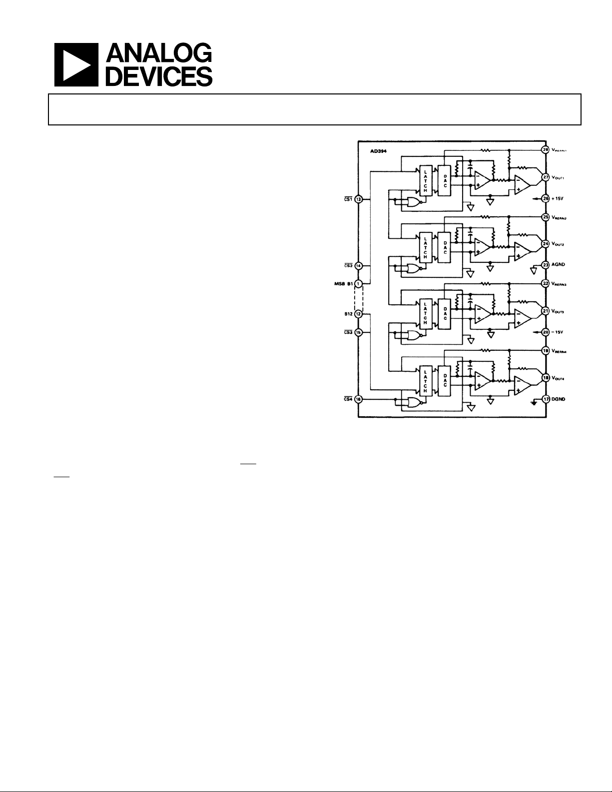
The AD394 contains four 12-bit, high-speed, low power, voltage
output, multiplying digital-to-analog converters in a compact
28-pin hybrid package. The design is based on a proprietary,
latched, 12-bit, CMOS DAC chip, which reduces chip count and
provides high reliability. The AD394 is ideal for systems
requiring digital control of many analog voltages where board
space is at a premium and low power consumption is a necessity. Such applications include automatic test equipment, process
controllers, and vector stroke displays.
(AD394T)
MAX
OUT
Quad 12-Bit D/A Converter
AD394
The AD394 is laser-trimmed to ±1/2 LSB maximum differential
and integral linearity (AD394T) and full-scale accuracy of
±0.05 percent at 25°C. The high initial accuracy is possible
because of the use of precision, laser-trimmed, thin-film scaling
resistors.
CS1
The individual DAC registers are accessed by the
CS4
control pins. These control signals allow any combination
through
of the DAC select matrix to occur (see Table 3). Once selected,
the DAC is loaded with a single 12-bit wide word. The 12-bit
parallel digital input interfaces to most 12- and 16-bit bus
systems.
The AD394 outputs (V
= 10 V) provide a ±10 V bipolar
REFIN
output range with positive-true offset binary input coding.
The AD394 is packaged in a 28-lead ceramic package and is
available for operation over a −55°C to +125°C temperature
range.
Figure 1. Functional Block Diagram
PRODUCT HIGHLIGHTS
1. The AD394 offers a dramatic reduction in printed circuit
board space in systems using multiple low power DACs.
2. Each DAC is independently addressable and provides
versatile control architecture for a simple interface to
microprocessors. All latch enable signals are leveltriggered.
3. The output voltage is trimmed to a full-scale accuracy of
±0.05%. Settling time to ±1/2 LSB is 15 µs maximum.
4. A maximum gain TC of 5 ppm/°C is achievable.
5. Two- or four-quadrant multiplication can be achieved
simply by applying the appropriate input voltage signal to
the selected DAC's reference (V
6. The AD394TD features guaranteed accuracy and linearity
over the −55°C to +125°C temperature range.
REFIN
).
Rev. A
Information furnished by Analog Devices is believed to be accurate and reliable.
However, no responsibility is assumed by Analog Devices for its use, nor for any
infringements of patents or other rights of third parties that may result from its use.
Specifications subject to change without notice. No license is granted by implication
or otherwise under any patent or patent rights of Analog Devices. Trademarks and
registered trademarks are the property of their respective owners.
One Technology Way, P.O. Box 9106, Norwood, MA 02062-9106, U.S.A.
Tel: 781.329.4700
Fax: 781.326.8703 © 2004 Analog Devices, Inc. All rights reserved.
www.analog.com
Page 2

AD394
TABLE OF CONTENTS
Specifications..................................................................................... 3
Analog Circuit Details ..................................................................8
Absolute Maximum Ratings............................................................ 5
ESD Caution.................................................................................. 5
Pin Configuration and Functional Block Diagram...................... 6
Theory of Operation ........................................................................ 7
Multiplying Mode ......................................................................... 7
Data and Control Signal Format ................................................7
Timing............................................................................................ 8
REVISION HISTORY
9/04–Rev. 0 Changed to Rev. A
Updated format....................................................................... Universal
Deleted AD395 part................................................................ Universal
Change to Product Description...........................................................1
Changes to Specifications table............................................................3
Delete Figure 3 .......................................................................................4
Delete Figure 6 .......................................................................................5
Change to Theory of Operation section.............................................7
Operation From ±12 V Supplies..................................................9
Power Supply Decoupling ............................................................9
Improving Full-Scale Stability .....................................................9
Applications ...................................................................................9
Applications ................................................................................ 10
Package Outline .............................................................................. 12
Ordering Guide .......................................................................... 12
7/85–Initial Version: Revision 0
Rev. A | Page 2 of 12
Page 3

AD394
SPECIFICATIONS
Table 1. TA = 25°C, V
Model Min Typ Max Units
DATA INPUTS (Pins 1-16)
TTL or 5 V CMOS-Compatible
Input Voltage
Bit ON (Logic 1) 2.4 5.5 V
Bit OFF (Logic 0) 0 0.8 V
Input Current ±4 ±40 µA
RESOLUTION 12 Bits
OUTPUT
Voltage Range
3
Current 5 mA
STATIC ACCURACY
Gain Error ±0.025 ±0.05 % of FSR
Offset ±0.012 ±0.025 % of FSR
Bipolar Zero ±0.012 % of FSR
Integral Linearity Error
Differential Linearity Error ±1/4 ±1/2 LSB
TEMPERATURE PERFORMANCE
Gain Drift ±5 ppm FSR/°C
Offset Drift ±5 ppm FSR/°C
Integrated Linearity Error5
T
to T
MIN
MAX
Differential Linearity Error
REFERENCE INPUTS
Input Resistance 5 25 kΩ
Voltage Range −11 +11 V
DYNAMIC PERFORMACE
Setting Time (to ±1/2 LSB)
V
= 10 V, Change All Digital Inputs from 5.0 V
PREFIN
to 0 V
V
= 0 V to 5 V Step, All Digital Inputs = 0 V 10 15 µs
REFIN
Reference Feedthrough Error See Figure 2
Digital-to-Analog Glitch Impulse
Crosstalk
Digital Input (Static)
Reference
8
POWER REQUIREMENTS
Supply Voltage
9
Current (All Digital Inputs 0 V or 5 V)
+V
S
−V
S
Power Dissipation 570 750 mW
= 10 V, VS = ±15 V, unless otherwise specified
REFIN
2
±V
5
±1/8 ±1/2 LSB
±1/4 ±1/2 LSB
10 15 µs
6
7
250 nV-s
0.1 LSB
2.0 mV p-p
±13.5 ±16.5 V
40 48 mA
18 28 mA
AD394TD and AD394TD/883B
REFIN
MONOTONICITY GUARANTEED
OVER FULL TEMPERATURE RANGE
1
V
4
Rev. A | Page 3 of 12
Page 4

AD394
AD394TD and AD394TD/883B
1
Model Min Typ Max Units
POWER SUPPLY GAIN SENSITIVITY
+V
−V
S
S
0.002 %FS/%
0.0025 %FS/%
TEMPERATURE RANGE
Operating (Full Specifications)
T −55 125 °C
Storage −65 150 °C
1
The AD394 T grade is available to MIL-STD-883, Method 5008, Class B. See Analog Devices Military Catalog (1985) for proper part number and detail specification.
2
Timing specifications appear in Table 5 and Figure 6.
3
See the Theory of Operation section for code tables and graphs.
4
FSR means full-scale range and is equal to 20 V for a ±10 V bipolar range and 10 V for a 0 V to 10 V unipolar range.
5
Integral nonlinearity is a measure of the maximum deviation from a straight line passing through the endpoints of the DAC transfer function.
6
This is a measure of the amount of charge injected from the digital inputs to the analog outputs when the inputs change state. It is usually specified as the area of the
glitch in nVs and is measured with V
7
Digital crosstalk is defined as the change in any one output’s steady state value as a result of any other output being driven from V
means of varying the digital input code.
8
Reference crosstalk is defined as the change in any one output as a result of any other output being driven from V
of varying the amplitude of the reference signal.
9
The AD394 can be used with supply voltages as low as ±11.4 V. See . Figure 10
= AGND.
REFIN
OUTMIN
to V
to V
OUTMIN
@10 kHz into a 2 kΩ load by means
OUTMAX
into a 2kΩ load by
OUTMAX
Rev. A | Page 4 of 12
Page 5

AD394
ABSOLUTE MAXIMUM RATINGS
Table 2.
Parameter Rating
+VS to DGND −0.3 V to +17 V
−VS to DGND −17 V to +0.3 V
Digital Inputs (Pins 1-16) to DNGD −0.3 V to +7 V
V
to DGND ±25 V
REFIN
AGND to DGND ±0.6 V
Analog Output (Pins 18, 21, 24, 27)
Indefinite short to AGND
or DGND momentary
short to ±V
S
ESD CAUTION
ESD (electrostatic discharge) sensitive device. Electrostatic charges as high as 4000 V readily accumulate on
the human body and test equipment and can discharge without detection. Although this product features
proprietary ESD protection circuitry, permanent damage may occur on devices subjected to high energy
electrostatic discharges. Therefore, proper ESD precautions are recommended to avoid performance
degradation or loss of functionality.
Stresses above those listed under “Absolute Maximum Ratings”
may cause permanent damage to the device. This is a stress
rating only and functional operation at or above this specification is not implied. Exposure to above maximum rating
conditions for extended periods may affect device reliability.
MIL-STD-883
The rigors of the military and aerospace environment, temperature extremes, humidity, mechanical stress, etc., demand the
utmost in electronic circuits. The AD394, with the inherent
reliability of an integrated circuit construction, was designed
with these applications in mind. The hermetically-sealed, low
profile DIP package takes up a fraction of the space required by
equivalent modular designs and protects the chips from
hazardous environments. To further insure reliability, the
AD394 is fully compliant to MIL-STD-833 Class B, Method
5008.
Figure 2. Feedthrough V
The Sine-Wave Digital Code Is Set at 1000 000 0000. Scale: Reference Input Is
5 V/DIV (Thin Trace). Feedthrough Output Is 5 mV/DIV. Time: 5 ms/DIV (Top
= 60 Hz (Top Photo) and 400 Hz (Bottom Photo).
REFIN
Photo), 500 µs/DIV (Bottom Photo).
Rev. A | Page 5 of 12
Page 6

AD394
PIN CONFIGURATION AND FUNCTIONAL BLOCK DIAGRAM
Figure 3. Pin Configuration
Figure 4. Functional Block Diagram (Bipolar)
Rev. A | Page 6 of 12
Page 7

AD394
THEORY OF OPERATION
The AD394 quad DAC provides four-quadrant multiplication.
It is a hybrid IC comprised of four, monolithic, 12-bit, CMOS,
multiplying DACs and eight precision output amplifiers. Each
of the four independent-buffered channels has an independent
reference input capable of accepting a separate dc or ac signal
for multiplying or for function generation applications. The
CMOS DACs act as digitally programmable attenuators when
used with a varying input signal or, if used with a fixed dc
reference, the DAC would act as a standard bipolar output DAC.
In addition, each DAC has a 12-bit wide data latch to buffer the
converter when connected to a microprocessor data bus.
REFIN
= 10 V
MULTIPLYING MODE
Figure 5 shows the transfer function. The diagram indicates an
area over which many different combinations of the reference
input and digital input can result in a particular analog output
voltage. The highlighted transfer line in the diagram indicates
the transfer function if a fixed reference is at the input. The
digital code above the diagram indicates the midpoint and
endpoints of each function. The relationship between the
reference input (V
output is given in Table 4. Note that the reference input signal
sets the slope of the transfer function (and determines the fullscale output at code 111...111), while the digital input selects the
horizontal position in each diagram.
), the digital input code, and the analog
REFIN
DATA AND CONTROL SIGNAL FORMAT
The AD394 accepts 12-bit parallel data in response to Control
Signals
lines are used to address the DAC register of interest. It is permissible to have more than one chip select active at any time. If
CS1–CS4
will be updated to the value located on the data bus. All control
inputs are level-triggered and may be hard-wired low to render
any register (or group of registers) transparent.
Table 3. DAC Select Matrix
CS1 CS2 CS3 CS4
Figure 5. The AD394 as a Four-Quadrant Multiplier
CS1–CS4
of Reference and Digital Input
. As detailed in Table 3, the four chip select
are all brought low coincident, all four DAC outputs
Operation
1 1 1 1 All DACs latched
0 1 1 1 Load DAC 1 from data bus
1 0 1 1 Load DAC 2 from data bus
1 1 0 1 Load DAC 3 from data bus
1 1 1 0 Load DAC 4 from data bus
0 0 0 0 All DACs simultaneously loaded
Table 4. Bipolar Code Table
Data Input Analog Output Analog Output Voltage, V
2047
⎫
1111 1111 1111 1 × (V
1100 0000 0000 1 × (V
1000 0000 0001 1 × (V
1000 0000 0000 1 × (V
0111 1111 1111 −1 × (V
0100 0000 0000 −1 × (V
0000 0000 0000 −1 × (V
REFIN
REFIN
REFIN
REFIN
REFIN
REFIN
REFIN
)
)
)
)
)
)
)
⎧
⎬
⎨
2048
⎭
⎩
1024
⎫
⎧
5.000 V 1/2 Scale
⎬
⎨
2048
⎭
⎩
1
⎫
⎧
4.88 mV 1 LSB
⎬
⎨
2048
⎭
⎩
0
⎧
⎫
⎨
⎬
2048
⎩
⎭
1
⎫
⎧
−4.88 mV −1LSB
⎬
⎨
2048
⎭
⎩
1024
⎫
⎧
−5.000 V −1/2 Scale
⎬
⎨
2048
⎭
⎩
2048
⎫
⎧
−10.000 V −Full Scale
⎬
⎨
2048
⎭
⎩
9.9951 V Full Scale − 1 LSB
0.000 V Zero
Rev. A | Page 7 of 12
Page 8

AD394
TIMING
The AD394 control signal timing is very straightforward.
CS4
must maintain a minimum pulse width of at least 400 ns
for a desired operation to occur. When loading data from a bus
into a 12-bit wide data latch, the data must be stable for at least
210 ns before returning CS to a high state. When
CS
data latch is transparent, allowing the data at the input to propagate through to the DAC. Data can change immediately after the
chip select returns high. DAC settling time is measured from
the falling edge of the active chip select.
Table 5. AD394 Timing Specifications, T
MIN
to T
Symbol Parameter Typ Units
t
CS
t
DA
t
DS
t
DH
Chip Select Pulse Width 170 ns min
Data Access Time 0 ns min
Data Setup Time 150 ns min
Data Hold Time 5 ns min
CS1
is low, the
MAX
–
the DAC outputs are accurately developed between the output
pin and Pin 23 (AGND), delivering these signals to remote
loads can be a problem. These problems are compounded if a
current booster stage is used, or if multiple packages are used.
Figure 8 illustrates the parasitic impedances that influence
output accuracy.
Figure 7. Recommended Ground Connections
Figure 6. Timing Diagram
ANALOG CIRCUIT DETAILS
Grounding Rules
The AD394 includes two ground connections to minimize
system accuracy degradation arising from grounding errors.
The two ground pins are designated DGND (Pin 17) and
AGND (Pin 23). The DGND pin is the return for the supply
current and serves as the reference point for the digital input
thresholds. Thus, DGND should be connected to the same
ground as the circuitry that drives the digital inputs.
Pin 23, AGND, is a high quality analog ground connection.
This pin should serve as the reference point for all analog
circuitry associated with the AD394. It is recommended that
any analog signal path carrying significant currents have its
own return connection to Pin 23, as shown in Figure 7.
Several complications arise in practical systems, particularly if
the load is referred to a remote ground. These complications
include dc gain errors due to wiring resistance between DAC
and load, noise due to currents from other circuits flowing in
power ground return impedances, and offsets due to multiple
load currents sharing the same signal ground returns. While
Figure 8. Grounding Errors in Multiple AD394 Systems
An output buffer configured as a subtracter, as shown in
Figure 9, can greatly reduce these errors. First, sensing the
voltage directly at the load with R4 eliminates the effects of
voltage drops in wiring resistance. Second, sensing the remote
ground directly with R3 eliminates the voltage drops caused by
currents flowing through Z
. Resistors R1 through R4 should
GA
be well matched to achieve maximum rejection of the voltage
appearing across Z
. Resistors matched to within 1 percent
GA
(including the effects of RW2 and RW3) reduce ground interaction errors by a factor of 100.
Rev. A | Page 8 of 12
Page 9

AD394
The AD2710 is a suitable reference source for such systems. It
features a guaranteed maximum temperature coefficient of
±1 ppm/°C. The combination of the AD2710LN and AD394, as
shown in Figure 11, yields a multiple DAC system with maximum full-scale drift of ±6 ppm/°C and excellent tracking.
Figure 9. Use of Subtracter Amplifier to Preserve Accuracy
OPERATION FROM ±12 V SUPPLIES
The AD394 may be used with ±12 V ±5% power supplies if
certain conditions are met. The most important limitation is the
output swing available from the output op amps. These amplifiers are capable of swinging only up to 3 V from either supply.
Thus, the normal ±10 V output range cannot be used. Changing
the output scale is accomplished by changing the reference
voltage. With a supply of ±11.4 V (5% less than ±12 V), the
output range is restricted to a maximum ±8.4 V swing. It may
be useful to scale the output at ±8.192 V (yielding a scale factor
of 4 mV per LSB).
Figure 10 shows a suggested circuit to set up a ±8.192 V output
range. To help prevent poor gain drift due to a possible mismatch between R
and R
IN
recommended to buffer R
of the divider network, it is
THEVENIN
, the potentiometer wiper voltage,
IN
with an OP-07.
Figure 10. Connections for ±8.192 V Full Scale
(Recommended for ±12 V Power Supplies)
POWER SUPPLY DECOUPLING
The power supplies used with the AD394 should be well-filtered
and regulated. Local supply decoupling consisting of a 10 µF
tantalum capacitor in parallel with 0.1 µF ceramic capacitor is
suggested. The decoupling capacitors should be connected
between the supply pins and the AGND pin. If an output
booster is used, its supplies should also be decoupled to the
load ground.
Figure 11. Low Drift Configuration
APPLICATIONS
Interfacing the AD394 to Microprocessors
The AD394 control logic provides a simple interface to microprocessors. The individual latches allow for multi-DAC interfacing to a single data bus.
16-Bit Processors
The AD394 is a 12-bit resolution DAC system and is easily
interfaced to 16-bit wide data buses. Several possible addressing
configurations exist.
In the circuit shown in Figure 12, a system write signal is used
to control the decoded address lines and a 74LS139 decoder
driven from the least significant address bits provides the
CS1
active-low
through
address lines A0 and A1 each select a single DAC of the four
contained in the AD394. The use of a separate address line for
each DAC allows several DACs to be accessed simultaneously.
The address lines are gated by the simultaneous occurrence of a
WR
system
and the appropriately decoded base address.
In the addressing scheme shown in Figure 12, A0 represents the
least significant word address bit. Data may reside in either the
12 MSBs (left-justified) or the 12 LSBs (right-justified). Left
justification is useful when the data-word represents a binary
fraction of full scale, while right-justified data usually represents
an integer value between 0 and 4095.
CS4
signals. In the circuit in Figure 12,
IMPROVING FULL-SCALE STABILITY
In large systems using multiple DACs, it may be desirable for all
devices to share a common reference. A precision reference can
greatly improve system accuracy and temperature stability.
Rev. A | Page 9 of 12
Figure 12. 16-Bit Bus Interface
Page 10

AD394
8-Bit Processors
The circuit of Figure 13 shows the general principles for
connecting the AD394 to an 8-bit data bus. The 74LS244 buffers
the data bus; its outputs are enabled when the DAC address
appears on the address bus. The first byte sent to the DAC is
loaded to the 74LS373 octal latch and, when the second byte is
sent to the DAC, it is combined with the first byte to create a
12-bit word. The connections shown are for right-hand justified
CS
data.
active, the DAC is loaded. Pull-up resistors at the output of the
74LS244 buffer ensure that the inputs to the DAC do not float at
an ill-defined level when the DAC is not being addressed. This
method of connecting 12-bit DACs to an 8-bit data bus is most
cost effective when multiple DACs are utilized for 8-bit data bus
applications.
and WR inputs to the DAC are also gated, and when
the ADC function since the processor can perform the required
digital operations under software control. A suitable circuit is
shown in Figure 14. The AD311 comparator compares the
unknown input voltage to one of the AD394 outputs for the
analog-to-digital conversion, while the other three outputs are
used as normal DACs. The diode clamp shown limits the
voltage swing at the comparator input and improves conversion
speed. With careful layout, a new compar-ison can be
performed in less than 15 µs, resulting in a 12-bit successive
approximation conversion in under 180 µs. The benefit of using
the AD394 in this application is that one ADC and three DACs
can be implemented with only two IC packages (the AD394 and
the comparator).
Figure 13. 8-Bit Data Bus Interface
APPLICATIONS
The functional density of the AD394 permits complex analog
functions to be produced under digital control, where board
space requirements would otherwise be prohibitive. Multipleoutput plotters, multichannel displays, complex waveform
generation, and multiple programmable voltage sources can all
be implemented with the AD394 in a fraction of the space that
would be needed if separate DACs were used.
Using the AD394 for Analog-to-Digital Conversion
Many systems require both analog output and analog input
capability. While complete integrated circuit analog-to-digital
converters (such as the AD574A) are readily available, the
AD394 can be used as the precision analog section of an ADC
if some external logic is available. Several types of analog-todigital converters can be built with a DAC, comparator, and
control logic, including staircase, tracking, and successiveapproximation types. In systems that include a micropro-cessor,
only a comparator must be added to the AD394 to accomplish
Figure 14. Using One AD394 Output for A/D Conversion
Programmable Window Comparator
The AD394 can be used to perform limit testing of responses to
digitally controlled input signals. For example, two DACs may
be used to generate software-controlled test conditions for a
component or circuit. The response to these input conditions
can be either completely converted from analog to digital or
simply tested against high and low limits generated by the two
DACs in the AD394.
Figure 15. Programmable Window Comparator
Used in Power-Supply Testing
In the circuit shown in Figure 15, two AD311 voltage comparators are used within the AD394 to test the output of a 5 V
power-supply regulator. The AD394 V
output (through an
OUT1
appropriate current booster) drives the input to the regulator to
simulate variations in input voltage. The output of the regulator
is applied to Comparators 1 and 2, with their outputs wire-
Rev. A | Page 10 of 12
Page 11

AD394
OR’ed with LED indicators as shown. The test limits for each
comparator are programmed by the AD394 V
OUT2
and V
OUT3
outputs. When the output of the device under testing is within
the limits, both comparators are off and D1 lights. If the output
is above or below the limits, either D4 or D5 lights.
AD394 as a Multiplier and Attenuator
So far, it has been assumed that the reference voltage V
fixed. In fact, V
−11 V < V
REFIN
can be any voltage within the range of
REFIN
< +11 V. It can be negative, positive, sinusoidal, or
REFIN
is
whatever the user prefers. This leads to the name “multiplying
D/A converters” because the output voltage, V
, is propor-
OUT
tional to the product of the digital input word and the voltage at
the V
terminal.
REFIN
OUT
()
V1V
REFIN
D
()
4096
()
4095 D 0
<<−=
D is the fractional binary value of the digital word applied to the
converter. The AD394 multiplies the digital input value by the
analog input voltage at V
for any value of V
REFIN
REFIN
up to
22 V p-p. This in itself is a powerful tool. Applications requiring
precision multiplication with minimal zero offset and very low
distortion should consider the AD394 as a candidate. One popular use for the AD394 is as an audio frequency attenuator. The
audio signal is applied to the V
input and the attenuation
REFIN
code is applied to the DAC; the output voltage is the product of
the two—an attenuated version of the input. The maximum
attenuation range obtainable utilizing 12 bits is 4096:1 or 72 dB.
Figure 16. AD394 as a Multiplier or Attenuator
Rev. A | Page 11 of 12
Page 12

AD394
PACKAGE OUTLINE
28
1.575 (40.01) MAX
15
0.810 (20.57)
0.770 (19.56)
1
PIN 1
SEE NOTE 1
0.225 (5.72)
MAX
0.145 (3.68)
MIN
0.023 (0.58)
0.014 (0.36)
NOTES
1. INDEX AREA; A NOTCH OR A LEAD ONE IDENTIFICATION MARK IS LOCATED ADJACENT TO LEAD ONE.
2. THE MINIMUM LIMIT FOR DIMENSION MAY BE 0.023" (0.58 mm) FOR ALL FOUR CORNER LEADS ONLY.
3. DIMENSION SHALL BE MEASURED FROM THE SEATING PLANE TO THE BASE PLANE.
4. THE BASIC PIN SPACING IS 0.100" (2.54 mm) BETWEEN CENTERLINES.
5. APPLIES TO ALL FOUR CORNERS.
6. MEASURED AT THE CENTERLINE OF THE LEADS.
7. TWENTY SIX SPACES.
8. CONTROLLING DIMENSIONS ARE IN INCHES. MILLIMETER DIMENSIONS ARE ROUNDED-OFF MILLIMETER
EQUIVALENTS FOR REFERENCE ONLY AND ARE NOT APPROPRIATE FOR USE IN DESIGN
0.100 (2.54)
BSC
SEE NOTE 4, 7
0.070 (1.78)
0.030 (0.76)
SEE NOTE 2
14
0.035 (0.89)
0.015 (0.38)
SEE NOTE 3
0.180 (4.57)
MIN
0.137 (3.48)
MAX
SEE NOTE 5
0.620 (15.75)
0.550 (13.97)
SEE NOTE 6
Figure 17. 28-Lead Bottom-Brazed Ceramic DIP for Hybrid [BBDIP/H]
(DH-28A)
Dimensions Shown in Inches and (Millimeters)
Note: Squared Corner and Dot in Shaded Area Indicate Pin 1.
ORDERING GUIDE
Model Temperature Range Gain Error Linearity Error (T
AD394TD −55°C to +125°C ±2 LSB ±1/2 LSB
AD394TD/883B −55°C to +125°C ±2 LSB ±1/2 LSB
0.015 (0.38)
0.008 (0.20)
MIN–TMAX
)
© 2004 Analog Devices, Inc. All rights reserved. Trademarks and
registered trademarks are the property of their respective owners.
C04851-0-9/04(A)
Rev. A | Page 12 of 12
 Loading...