

Page 1
Three-Phase
I
S1
Vds
Vqs
SECTOR
MULTIPLIER
SINE AND
COSINE
MULTIPLIER
INPUT
DATA
STROBE
HOMOPOLAR
OUTPUT
HOMOPOLAR
REFERENCE
+5V GND –5V
φ
POSITION
PARALLEL
DATA
12 BITS
3
φ-2φ
Cos (θ + 120°)
Cos (θ + 240°)
SinθCosθ
Cosθ
Sinθ
Cos θ + φ
CONV1
CONV2
DECODE
BUSY
Vds'
Vqs'
Sin
θ + φ
SECTOR
MULTIPLIER
SINE AND
COSINE
MULTIPLIER
Ia + Ib + Ic
3
I
S2
I
S3
a
FEATURES
Current Conditioning
Complete Vector Transformation on Silicon
Three-Phase 120° and Orthogonal 90° Signal
Transformation
Three-Phase Balance Diagnostic–Homopolar Output
DQ Manipulation
Real-Time Filtering
APPLICATIONS
AC Induction Motor Control
Spindle Drive Control
Pump Drive Control
Compressor Drive Control and Diagnostics
Harmonic Measurement
Frequency Analysis
Three-Phase Power Measurement
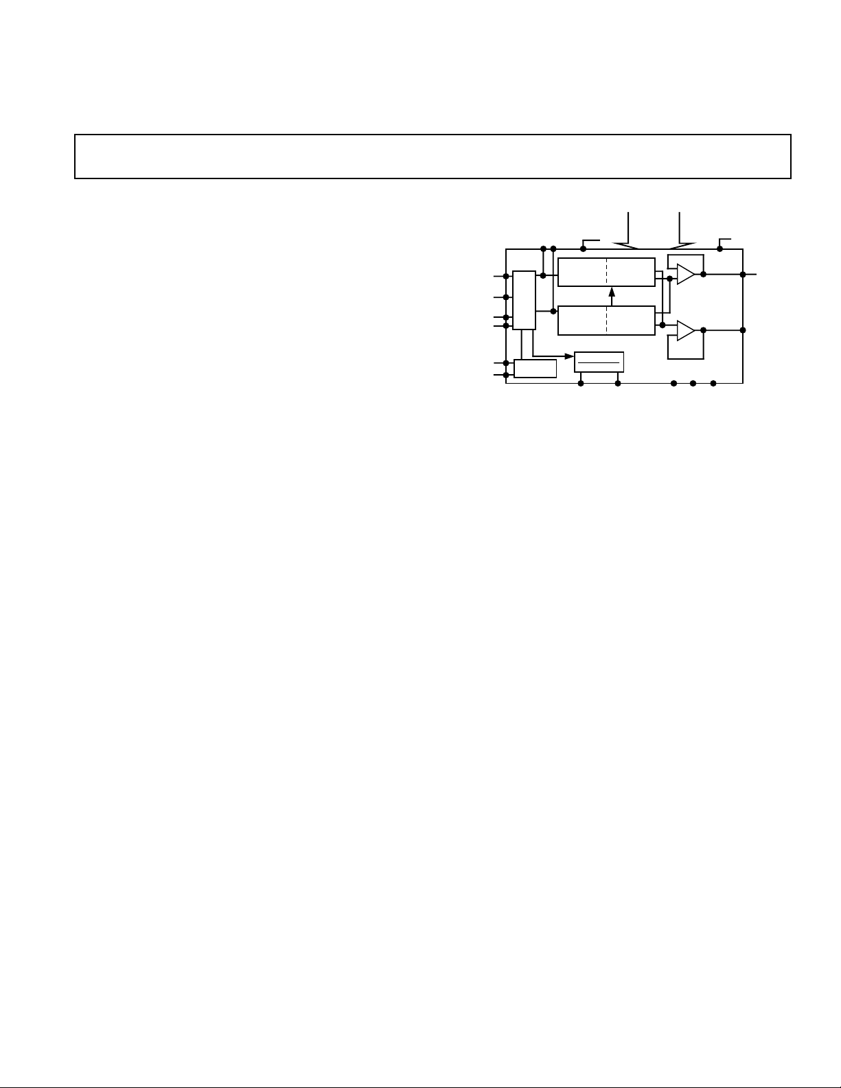
GENERAL DESCRIPTION
The AD2S105 performs the vector rotation of three-phase 120
degree or two-phase 90 degree sine and cosine signals by transferring these inputs into a new reference frame which is controlled
by the digital input angle φ. Two transforms are included in the
AD2S105. The first is the Clarke transform which computes
the sine and cosine orthogonal components of a three-phase input. These signals represent real and imaginary components
which then form the input to the Park transform. The Park
transform relates the angle of the input signals to a reference
frame controlled by the digital input port. The digital input
port on the AD2S105 is a 12-bit/parallel natural binary port.
If the input signals are represented by Vds and Vqs, respectively,
where Vds and Vqs are the real and imaginary components, then
the transformation can be described as follows:
Vds' = Vds Cosφ – Vqs Sinφ
Vqs' = Vds Sinφ + Vqs Cosφ
Where Vds' and Vqs' are the output of the Park transform
and Sinφ, and Cosφ are the trigonometric values internally calculated by the AD2S105 from the binary digital data φ.
The input section of the device can be configured to accept
either three-phase inputs, two-phase inputs of a three-phase
system, or two 90 degree input signals. The homopolar output
indicates an imbalance of a three-phase input only at a userspecified level.
The digital input section will accept a resolution of up to 12 bits.
An input data strobe signal is required to synchronize the position
data and load this information into the device counters.
REV. 0
Information furnished by Analog Devices is believed to be accurate and
reliable. However, no responsibility is assumed by Analog Devices for its
use, nor for any infringements of patents or other rights of third parties
which may result from its use. No license is granted by implication or
otherwise under any patent or patent rights of Analog Devices.
Current Conditioner
AD2S105
FUNCTIONAL BLOCK DIAGRAM
A two-phase rotated output facilitates the implementation of
multiple rotation blocks.
The AD2S105 is fabricated on LC
±5 volt power supplies.
PRODUCT HIGHLIGHTS
Current Conditioning
The AD2S105 transforms the analog stator current signals (I
I
, I
) using the digital angular signal (reference frame) into dc
2
3
s
s
values which represent direct current (I
rent (I
). This transformation of the ac signals into dc values
qs
simplifies the design of the analog-to-digital (A/D) conversion
scheme. The A/D conversion scheme is simplified as the bandwidth sampling issues inherent in ac signal processing are
avoided and in most drive designs, simultaneous sampling of the
stator currents may not be necessary.
Hardware Peripheral for Standard Microcontroller and DSP
Systems
The AD2S105 off-loads the time consuming Cartesian transformations from digital processors and benchmarks show a significant speed improvement over single processor designs. AD2S105
transformation time = 2 µs.
Field Oriented Control of AC Motors
The AD2S105 accommodates all the necessary functions to provide a hardware solution for current conditioning in variable
speed control of ac synchronous and asynchronous motors.
Three-Phase Imbalance Detection
The AD2S105 can be used to sense imbalances in a three-phase
system via the homopolar output.
One Technology Way, P.O. Box 9106, Norwood. MA 02062-9106, U.S.A.
Tel: 617/329-4700 Fax: 617/326-8703
2
MOS and operates on
) and quadrature cur-
ds
,
s1
Page 2

(VDD = +5 V ± 5%; VSS = –5 V ± 5% AGND = DGND = O V;
AD2S105–SPECIFICATIONS
TA = –40°C to +85°C, unless otherwise noted)
Parameter Min Typ Max Units Conditions
SIGNAL INPUTS
PH/IP1, 2, 3, 4 Voltage Level ±2.8 ±3.3 V p-p DC to 50 kHz
PH/IPH1, 2, 3 Voltage Level ±4.25 V p-p DC to 50 kHz
Input Impedance
PH/IP1, 2, 3 7.5 10 kΩ
PH/IPH1, 2, 3 13.5 18 kΩ
PH/IP1, 4 1 MΩ Mode 1 Only (2 Phase)
Sin & Cos
Gain
PH/IP1, 2, 3, 4 0.95 1 1.05
PH/IPH1, 2, 3 0.56
VECTOR PERFORMANCE
3-Phase Input-Output
Radius Error (Any Phase) ±0.4 ±1 % DC to 600 Hz
Angular Error
1, 2
PH/IP 15 30 arc min DC to 600 Hz
PH/IPH 30 arc min DC to 600 Hz
Differential Nonlinearity ±1 LSB
Full Power Bandwidth 50 kHz
Small Signal Bandwidth 200 kHz
ANALOG SIGNAL OUTPUTS
PH/OP1, 4 PH/IP, PH/IPH INPUTS
Output Voltage
3
±2.8 ±3.3 V p-p DC to 50 kHz
Offset Voltage 2 10 mV Inputs = 0 V
Slew Rate 2 V/µs
Small Signal Step Response 1 µs1° Input to Settle to
±1 LSB (Input to Output)
Output Impedance 15 Ω
Output Drive Current 3.0 4.0 mA Outputs to AGND
Resistive Load 2 kΩ
Capacitive Load 50 pF
STROBE
Write 100 ns Positive Pulse
Max Update Rate 366 kHz
BUSY
Pulse Width 1.7 2.5 µs Conversion in Process
V
OH
V
OL
4V dcI
1V dcI
= 0.5 mA
OH
= 0.5 mA
OL
DIGITAL INPUTS
DB1–DB12
V
IH
V
IL
Input Current, I
IN
Input Capacitance, C
IN
3.5 V dc
1.5 V dc
±10 µA
10 pF
CONV MODE
(CONV1, CONV2)
V
IH
V
IL
3.5 V dc
1.5 V dc
Input Current 100 µA Internal 50 kΩ
Input Capacitance 10 pF Pull-Up Resistor
–2–
REV. 0
Page 3

AD2S105
WARNING!
ESD SENSITIVE DEVICE
Parameter Min Typ Max Units Conditions
HOMOPOLAR OUTPUT
HPOP–OUTPUT
V
OH
V
OL
HPREF–REFERENCE 0.5 V dc Homopolar Output-Internal
POWER SUPPLY
V
DD
V
SS
I
DD
I
SS
NOTES
1
Angular accuracy includes offset and gain errors, measured with a stationary digital input and maximum analog frequency inputs.
2
The angular error does not include the additional error caused by the phase delay as a function of input frequency. For example, if f
to the error due to phase delay is: 650 ns × f
3
Output subject to input voltage and gain.
Specifications subject to change without notice.
× 60 × 360 = 8.4 arc minutes.
INPUT
4V dcI
1V dcI
= 0.5 mA
OH
= 0.5 mA
OL
I
= 25 µA and 20 kΩ to AGND
SOURCE
4.75 5 5.25 V dc
–5.25 –5 –4.75 V dc
4 10 mA Quiescent Current
4 10 mA Quiescent Current
= 600 Hz, the contribution
INPUT
RECOMMENDED OPERATING CONDITIONS
Power Supply Voltage (+VDD, –V
) . . . . . . . . . ±5 V dc ± 5%
SS
Analog Input Voltage (PH/IP1, 2, 3, 4) . . . . . . 2 V rms ± 10%
Analog Input Voltage (PH/IPH1, 2, 3) . . . . . . 3 V rms ± 10%
Ambient Operating Temperature Range
Industrial (AP) . . . . . . . . . . . . . . . . . . . . . . .–40°C to +85°C
ABSOLUTE MAXIMUM RATINGS (TA = +25°C)
VDD to AGND . . . . . . . . . . . . . . . . . . . . . . . –0.3 V to +7 V dc
V
to AGND . . . . . . . . . . . . . . . . . . . . . . . +0.3 V to –7 V dc
SS
AGND to DGND . . . . . . . . . . . . . . . . . . . . . . . . . . . ±0.3 V dc
Analog Input Voltage to AGND . . . . . . . . . . . . . . . V
Digital Input Voltage to DGND . . . . –0.3 V to V
Digital Output Voltage to DGND . . . . . . –0.3 V to V
to V
SS
+ 0.3 V dc
DD
DD
DD
+ V dc
Analog Output Voltage to AGND
. . . . . . . . . . . . . . . . . . . . . . V
– 0.3 V to VDD + 0.3 V dc
SS
Analog Output Load Condition (PH/OP1, 4
Sinθ, Cosθ) . . . . . . . . . . . . . . . . . . . . . . . . . . . . . . . . . . . . . . . 2 kΩ
Power Dissipation . . . . . . . . . . . . . . . . . . . . . . . . . . . .140 mW
Operating Temperature
Industrial (AP) . . . . . . . . . . . . . . . . . . . . . . . –40°C to +85°C
Storage Temperature . . . . . . . . . . . . . . . . .–65°C to +150°C
Lead Temperature (Soldering, 10 sec) . . . . . . . . . . . . . +300°C
CAUTION
1. Absolute Maximum Ratings are those values beyond which
damage to the device will occur.
2. Correct polarity voltages must be maintained on the +V
DD
and –VSS pins
ORDERING GUIDE
Model Temperature Range Accuracy Option*
AD2S105AP –40°C to +85°C 30 arc min P-44A
*P = Plastic Leaded Chip Carrier.
CAUTION
ESD (electrostatic discharge) sensitive device. Electrostatic charges as high as 4000 V readily
accumulate on the human body and test equipment and can discharge without detection.
Although the AD2S105 features proprietary ESD protection circuitry, permanent damage may
occur on devices subjected to high energy electrostatic discharges. Therefore, proper ESD
precautions are recommended to avoid performance degradation or loss of functionality.
REV. 0
–3–
Page 4
AD2S105
6 5 4 3 2 1 44 43 42 41 40
18 19 20 21 22 23 24 25 26 27 28
29
30
31
32
33
34
35
36
37
38
39
V
SS
V
DD
STROBE
NC
NC
BUSY
DGND
V
DD
NC
NC
V
SS
HPREF
HPOP
CONV1
CONV2
COS
DB12
HPFILT
DB11
NC = NO CONNECT.
TOP VIEW
(NOT TO SCALE)
AD2S105
PH/OP4
NC
SIN
7
8
11
12
13
14
15
16
17
9
10
NC
DB1
DB2
DB3
DB4
DB5
DB6
DB7
DB8
DB9
DB10
PH/OP1
NC
NC
AGND
PH/IP4
PH/IPH3
PH/IP3
PH/IPH2
PH/IP2
PH/IPH1
PH/IP1
PIN DESIGNATIONS
1, 2, 3
Pin Mnemonic Description
3 STROBE Begin Conversion
4V
5V
DD
SS
Positive Power Supply
Negative Power Supply
6 PH/OP4 Sin (θ + φ)
7 PH/OP1 Cos (θ + φ)
10 AGND Analog Ground
11 PH/IP4 Sin θ Input
12 PH/IPH3 High Level Cos
(θ + 240°) Input
13 PH/IP3 Cos (θ + 240°) Input
14 PH/IPH2 High Level Cos
(θ + 120°) Input
15 PH/IP2 Cos (θ + 120°) Input
16 PH/IPH1 High Level Cos θ Input
17 PH/IP1 Cos (θ) Input
19 V
SS
Negative Power Supply
20 HPREF Homopolar Reference
21 HPOP Homopolar Output
22 HPFILT Homopolar Filter
23 CONV1 Select Analog Input
Format
24 CONV2 Select Analog Input
Format
25 COS Cos Output
26 SIN Sin Output
27–38 DB12 to DB1 (DB1 = MSB, DB12 =
LSB Parallel Input Data)
41 V
DD
Positive Power Supply
42 DGND Digital Ground
44 BUSY Internal Logic Setup
Time
NOTES
1
90° orthogonal signals = Sin θ, Cos θ (Resolver) = PH/IP4 and PH/IP1.
2
Three phase, 120°, three-wire signals = Cos θ, Cos (θ + 120°), Cos (θ + 240°).
= PH/IP1, PH/IP2, PH/IP3
High Level = PH/IPH1, PH/IPH2, PH/IPH3.
3
Three Phase, 120°, two-wire signals = Cos (θ + 120°), Cos (θ + 240°) =
PH/IP2, PH/IP3.
In all cases where any of the input Pins 11 through 17 are not used, they must
be left unconnected.
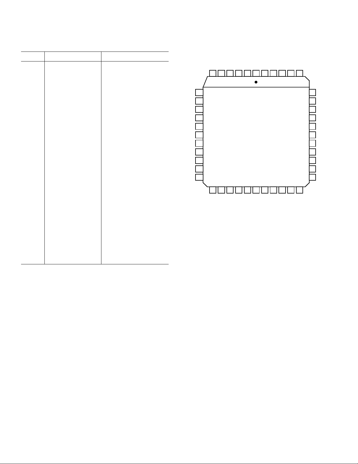
PIN CONFIGURATION
–4–
REV. 0
Page 5

AD2S105
I
ds
I
qs
Ids'
I
qs
'
φ
e
j
φ
THEORY OF OPERATION
A fundamental requirement for high quality induction motor
drives is that the magnitude and position of the rotating air-gap
rotor flux be known. This is normally carried out by measuring
the rotor position via a position sensor and establishing a rotor
oriented reference frame.
To generate a flux component in the rotor, stator current is applied. A build-up of rotor flux is concluded which must be
maintained by controlling the stator current, i
, parallel to the
ds
rotor flux. The rotor flux current component is the magnetizing
current, i
mr
.
Torque is generated by applying a current component which is
perpendicular to the magnetizing current. This current is normally called the torque generating current, i
qs
.
To orient and control both the torque and flux stator current
vectors, a coordinate transformation is carried out to establish a
new reference frame related to the rotor. This complex calculation is carried out by the AD2S105.
To expand upon the vector operator a description of a single
vector rotation is of assistance. If it is considered that the
moduli of a vector is OP and that through the movement of rotor position by f, we require the new position of this vector it
can be deduced as follows:
Let original vector OP = A (Cos u + jSIN u) where A is a
constant;
if OQ = OP e
and: e
jF
jF
= Cos f + jSin f
(1)
OQ = A (Cos (u + f) + jSin (u + f))
= A [Cos u Cos φ – Sin u Sin φ + jSin u Cos φ + jCos u Sin φ]
= A [(Cos u + jSin u) (Cos f + jSin f)] (2)
a
Q
θ + φ
φ
O
P
θ
d
To relate these stator current to the reference frame the rotor
currents assume the same rectangular coordinates, but are now
rotated by the operator e
jf
, where ejf = Cos f + jSin f.
Here the term vector rotator comes into play where the stator
current vector can be represented in rotor-based coordinates or
vice versa.
The AD2S105 uses e
mathematical function, it rotates the orthogonal i
jf
as the core operator. In terms of the
and iqs com-
ds
ponents as follows:
i
' + jiqs' = (Ids + jIqs) e
ds
jf
where ids', iqs' = stator currents in the rotor reference frame. And
jf
= Cos f + jSin f
e
+ jIqs)(Cos f + jSin f)
= (I
ds
The output from the AD2S105 takes the form of:
' = Ids Cos f – Iqs Sin f
i
ds
' = Ids Sin f + Iqs Cos f
i
qs
The matrix equation is:
ids']
[
iqs'
Cos f – Sin f
=
[
Sin f
Cos f I
I
ds
][
]
qs
and it is shown in Figure 2.
Figure 2. AD2S105 Vector Rotation Operation
INPUT CLARK
COSθ COSθ + 120° COS θ + 240°
SINθ
3φ TO 2φ
TRANSFORMATION
PARK
SINE AND
COSINE
MULTIPLIER
(DAC)
SINE AND
COSINE
MULTIPLIER
(DAC)
COS (θ + φ)
SIN (θ + φ)
Figure 1. Vector Rotation in Polar Coordinate
The complex stator current vector can be represented as is = i
+ aibs + a2ics where a = e
j2π
3
and a2 = e
j4π
. This can be re-
3
as
placed by rectangular coordinates as
In this equation i
= ids + ji
i
s
and iqs represent the equivalent of a two-
ds
qs
(3)
phase stator winding which establishes the same magnitude of
MMF in a three-phase system. These inputs can be seen after
the three-phase to two-phase transformation in the AD2S105
LATCH
DIGITAL
LATCH
φ
LATCH
Figure 3. Converter Operation Diagram
block diagram. Equation (3) therefore represents a three-phase
to two-phase conversion.
REV. 0
–5–
Page 6

AD2S105
CONVERTER OPERATION
The architecture of the AD2S105 is illustrated in Figure 3. The
AD2S105 is configured in the forward transformation which rotates the stator coordinates to the rotor reference frame.
Vector Rotation
Position data, f, is loaded into the input latch on the positive
edge of the strobe pulse. (For detail on the timing, please refer
to the “timing diagram.”) The negative edge of the strobe signifies that conversion has commenced. A busy pulse is subsequently produced as data is passed from the input latches to the
Sin and Cos multipliers. During the loading of the multiplier,
the busy pulse remains high preventing further updates of f in
both the Sin and Cos registers.
The negative edge of the busy pulse signifies that the multipliers
are set up and the orthogonal analog inputs are then multiplied
real time. The resultant two outputs are accessed via the
PH/OP1 (Pin 7) and PH/OP4 (Pin 6).
For other configurations, please refer to “Transformation
Configuration.”
CONNECTING THE CONVERTER
Power Supply Connection
The power supply voltages connected to VDD and VSS pins
should be +5 V dc and –5 V dc and must not be reversed. Pin 4
(V
) and Pin 41 (VDD) should both be connected to +5 V;
DD
similarly, Pin 5 (V
) and Pin 19 (VSS) should both be con-
SS
nected to –5 V dc.
It is recommended that decoupling capacitors, 100 nF (ceramic)
and 10 µF (tantalum) or other high quality capacitors, are con-
nected in parallel between the power line V
, VSS and AGND
DD
adjacent to the converter. Separate decoupling capacitors should
be used for each converter. The connections are shown in Figure 4.
+5V
DD
V
AD2S105
TOP VIEW
1
23
DD
V
GND
10µF
–5V
10µF
SS
100nF
+
+
100nF
V
AGND
12 34
SS
V
Figure 4. AD2S105 Power Supply Connection
ANALOG SIGNAL INPUT AND OUTPUT CONNECTIONS
Input Analog Signals
All analog signal inputs to AD2S105 are voltages. There are two
different voltage levels of three-phase (0°, 120°, 240°) signal inputs. One is the nominal level, which is ± 2.8 V dc or 2 V rms
and the corresponding input pins are PH/IP1 (Pin 17), PH/IP2
(Pin 15), PH/IP3 (Pin 13) and PH/IP4 (Pin 11).
The high level inputs can accommodate voltages from nominal
up to a maximum of ±V
. The corresponding input pins
DD/VSS
are PH/IPH1 (Pin 16), PH/IPH2 (Pin 14) and PH/IPH3 (Pin
12). The homopolar output can only be used in the three-phase
connection mode.
The converter can accept both two-phase format and threephase format input signals. For the two-phase format input, the
two inputs must be orthogonal to each other. For the threephase format input, there is the choice of using all three inputs
or using two of the three inputs. In the latter case, the third input signal will be generated internally by using the information
of other two inputs. The high level input mode, however, can
only be selected with three-phase/three-input format. All these
different conversion modes, including nominal/high input level
and two/three-phase input format can be selected using two select pins (Pin 23, Pin 24). The functions are summarized in
Table I.
Table I. Conversion Mode Selection
CONV1 CONV2
Mode Description (Pin 23) (Pin 24)
MODE1 2-Phase Orthogonal with 2 Inputs NC DGND
Nominal Input Level
MODE2 3-Phase (0°, 120°, 240°) with 3 Inputs DGND V
Nominal/High Input Level*
MODE3 3-Phase (0°, 120°, 240°) with 2 Inputs V
Nominal Input Level
*The high level input mode can only be selected with MODE2.
DD
DD
V
DD
MODE1: 2-Phase/2 Inputs with Nominal Input Level
In this mode, PH/IP1 and PH/IP4 are the inputs and the Pins
12 through 16 must be left unconnected.
MODE2: 3-Phase/3 Inputs with Nominal/High Input Level
In this mode, either nominal or high level inputs can be used.
For nominal level input operation, PH/IP1, PH/IP2 and PH/IP3
are the inputs, and there should be no connections to PH/IPH1,
PH/IPH2 and PH/IPH3; similarly, for high level input operation, the PH/IPH1, PH/IPH2 and PH/IPH3 are the inputs, and
there should be no connections to PH/IP1, PH/IP2 and PH/IP3.
In both cases, the PH/IP4 should be left unconnected. For high
level signal input operation, select MODE2 only.
MODE3: 3-Phase/2 Inputs with Nominal Input Level
In this mode, PH/IP2 and PH/IP3 are the inputs and the third
signal will be generated internally by using the information of
other two inputs. It is recommended that PH/IP1, PH/IPH1,
PH/IPH2, PH/IP4 and PH/IPH3 should be left unconnected.
–6–
REV. 0
Page 7

AD2S105
Output Analog Signals
There are two sets of analog output from the AD2S105.
Sin/Cos orthogonal output signals are derived from the Clark/
three-to-two-phase conversion before the Park angle rotation.
These signals are available on Pin 25 (Cos u) and Pin 26 (Sin
u), and occur before Park angle rotation.
Two-Phase (Sin (u + f), Cos (u + f)) Signals
These represent the output of the coordinate transformation.
These signals are available on Pin 6 (PH/OP4, Sin (u + f)) and
Pin 7 (PH/OP1, Cos (u + f)).
HOMOPOLAR OUTPUT
HOMOPOLAR Reference
In a three-phase ac system, the sum of the three inputs to the
converter can be used to indicate whether or not the phases are
balanced.
If V
= PH/IP1 + PH/IP2 + PH/IP3 (or PH/IPH1 + PH/
SUM
IPH2 + PH/IPH3) this can be rewritten as V
= [Cosu, +
SUM
Cos (u + 120°) + Cos (u + 240°)] = 0. Any imbalances in the
line will cause the sum V
output (HPOP) goes high when V
≠ 0. The AD2S105 homopolar
SUM
SUM
> 3 × V
. The voltage
ts
level at which the HPOP indicates an imbalance is determined
by the HPREF threshold, V
. This is set internally at ±0.5 V dc
ts
(±0.1 V dc). The HPOP goes high when
(Cosθ+Cos(θ+120°)+ Cos(θ+240°))
Vts<
3
×V
where V is the nominal input voltage.
With no external components V
must exceed ±1.5 V dc in
SUM
order for HPOP to indicate an imbalance. The sensitivity of the
threshold can be reduced by connecting an external resistor between HPOP and ground in Figure 5 where
0.5 R
EXT
EXT
+20,000
R
EXT
is in Ω.
Vts=
R
Example: From the equivalent circuit, it can be seen that the inclusion of a 20 kΩ resistor will reduce V
to ±0.25 V dc. This
ts
corresponds to an imbalance of ±0.75 V dc in the inputs.
Homopolar Filtering
The equation V
= 0 denotes an imbalance when V
= Cosu + Cos (u + 120°) + Cos (u + 240°)
SUM
≠ 0. There are conditions,
SUM
however, when an actual imbalance will occur and the conditions as defined by V
will be valid. For example, if the first
SUM
phase was open circuit when u = 90° or 270°, the first phase is
valid at 0 V dc. V
is valid, therefore, when Cosu is close to 0.
SUM
In order to detect an imbalance u has to move away from 90° or
270°, i.e., when on a balanced line Cos u ≠ 0.
Line imbalance is detected as a function of HPREF, either set
by the user or internally set at ± 0.5 V dc. This corresponds to a
dead zone when f = 90° or 270° ± 30°, i.e., V
= 0, and,
SUM
therefore, no indicated imbalance. If an external 20 kΩ resistor
is added, this halves V
and reduces the zone to ±15°. Note this
ts
example only applies if the first phase is detached.
In order to prevent this false triggering an external capacitor
needs to be placed from HPFILT to ground, as shown in Figure
5. This averages out the perceived imbalance over a complete
cycle and will prevent the HPOP from alternatively indicating
balance and imbalance over u = 0° to 360°.
For
dθ
=1000 rpm C
dt
dθ
=100 rpm C
dt
EXT
EXT
= 220 nF
= 2. 2 µF
Note: The slower the input rotational speed, the larger the time
constant required over which to average the HPOP output. Use
of the homopolar output at slow rotational speeds becomes impractical with respect to the increased value for C
34
EXT
.
25µA
HOMOPOLAR
REFERENCE
EXTERNAL
RESISTOR
TO TRIGGER
20kΩ
Figure 5. The Equivalent Homopolar Reference Input
Circuitry
REV. 0
–7–
DGND
AD2S105
TOP VIEW
1
HPFILT
HPOP
HPREF
AGND
12
C
EXT
23
220nF
HPOP
HPREF
R
EXT
GND
Figure 6. AD2S105 Homopolar Output Connections
Page 8

AD2S105
THREE PHASE INPUT
AD2S105
TOP VIEW
141
38
30
27
23
12
16
DIGITAL ANGLE INPUT
LSB
SIN
COS
10µF
100nF
10µF100nF
–5V
+5V
GND
TWO PHASE OUTPUT
STROBE
BUSY
HPOP
HPFILT
HPREF
MSB
PH/OP1
AGND
PH/IP4
PH/IP3
PH/IP2
PH/IP1
34
TIMING DIAGRAMS
Busy Output
The BUSY output will go HI at the negative edge of the
STROBE input. This is used to synchronize digital input data
and load the digital angular rotation information into the device
counter. The BUSY output will remain HI for 2 µs, and go LO
until the next strobe negative edge occurs.
Strobe Input
The width of the positive STROBE pulse should be at least
100 ns, in order to successfully start the conversion. The maximum frequency of STROBE input is 366 kHz, i.e., there should
be at least 2.73 µs from the negative edge of one STROBE pulse
to the next rising edge. This is illustrated by the following timing diagram and table.
t
STROBE
BUSY
t
1
t
2
t
r
4
t
f
t
3
Figure 7. AD2S105 Timing Diagram
Note: Digital data should be stable 25 ns before and after positive strobe edge.
Table II. AD2S105 Timing Table
Parameter Min Typ Max Condition
t
1
t
2
t
3
t
4
t
r
100 ns STROBE Pulse Width
30 ns STROBE ↓ to BUSY ↑
1.7 µs 2.5 µs BUSY Pulse Width
100 ns BUSY ↓ to STROBE ↑
20 ns BUSY Pulse Rise Time
with No Load
150 ns BUSY Pulse Rise Time
with 68 pF Load
t
f
10 ns BUSY Pulse Fall Time
with No Load
120 ns BUSY Pulse Fall Time
with 68 pF Load
TYPICAL CIRCUIT CONFIGURATION
Figure 8 shows a typical circuit configuration for the AD2S105
in a three phase, nominal level input mode (MODE2).
Figure 8. Typical Circuit Configuration
APPLICATIONS
Transformation Configuration
The AD2S105 can perform both forward and reverse transformations. The section “Theory of Operation” explains how the
chip operates with the core operator e
ward transformation. The reverse transformation, e
+jf
, which performs a for-
–jf
, is per-
formed by providing a negative angle φ. Figure 9 shows two
different phase input/output connections for AD2S105 reverse
transformation operation.
2 PHASE – 2 PHASE
3 PHASE – 2 PHASE
Figure 9. Forward and Reverse Transformation Connections
FORWARD
TRANSFORMATION
AD2S105
Cosθ Cos(θ + φ)
Sinθ
Cosθ
Cos(θ + 120°)
Cos(θ + 240°)
REVERSE
TRANSFORMATION
AD2S105
+j
φ
e
Sin(θ + φ)
Cos(θ + φ)
+j
φ
e
Sin(θ + φ)
Cosθ
Sinθ
Cosθ
Cos(θ + 120°)
Cos(θ + 240°)
–j
φ
e
–j
φ
e
–8–
Cos(θ – φ)
Sin(θ – φ)
Cos(θ – φ)
Sin(θ – φ)
–1
REV. 0
Page 9

AD2S105
MEASUREMENT OF HARMONICS
In ac power systems, the quality of the electrical supply can be
affected by harmonic voltages injected into the power main by
loads, such as variable speed drive systems and computer power
supplies. These harmonics are injected into other loads through
the point of common coupling of the supply. This produces extra losses in power factor correction capacitors, power supplies
and other loads which may result in failure. It also can result in
tripping and failure of computer systems and other sensitive
equipment. In ac machines the resultant harmonic currents and
flux patterns produce extra motor losses and torque pulsations,
which can be damaging to the load.
The AD2S105 can be used to monitor and detect the presence
and magnitude of a particular harmonic on a three-phase line.
Figure 10 shows the implementation of such a scheme using the
AD2S105, where Va, Vb, Vc are the scaled line voltages.
Va
Vb
TRANSFORMATION
Vc
AD2S105
THREE -TO-TWO
CLARK
HOMOPOLAR
OUTPUT
Vd
TRANSFORMATION
Vq
12-BIT UP/DOWN
COUNTER
jφ
PARK
e
1
Vd
LOW PASS
1
Vq
PULSE INPUTS
DIRECTION
FILTER
a
k
Figure 10. Harmonics Measurement Using AD2S105
Selecting a harmonic is achieved by synchronizing the rotational
frequency of the park digital input, f, with the frequency of the
fundamental component and the integer harmonic selected. The
update rate, r, of the counters is determined by:
r = 4096 ×
n ×ω
2π
.
Here, r = input clock pulse rate (pulses/second);
n = the order of harmonics to be measured;
v = fundamental angular frequency of the ac signal.
The magnitude of the n-th harmonic as well as the fundamental
component in the power line is represented by the output of the
low-pass filter, a
. In concert with magnitude of the harmonic
k
the AD2S105 homopolar output will indicate whether the three
phases are balanced or not. For more details about this application, refer to the related application note listed in the
bibliography.
Field Oriented Control of AC Induction Motors
In ac induction motors, torque is produced through interaction
between the rotating air gap field and currents induced in the
rotor windings. The stator currents consist of two components,
the flux component which drives the air gap field, and the
torque component which is reflected from the rotor windings. A
successful field oriented control strategy must independently
control the flux component of current, referred to as direct current (I
rent, referred to as quadrature current (I
), and the torque producing component of stator cur-
ds
qs
).
The control architecture in Figure 11 is referred to as field oriented because the control algorithms performed on the ADSP2105 processor operate on decoupled flux and torque current
components in a reference frame relative to the rotor flux of the
motor. The control algorithms provide fast torque response at
any speed which results in superior dynamic performance, and
consequently, load variations have minimal effect on speed or
position control.
The AD2S90 resolver-to-digital converter is used to convert the
modulated resolver position signals into a 12-bit digital position
value. This value is brought into the ADSP-2105 via the
serial port where the control algorithms calculate the rotor flux
angle. The rotor flux angle is the sum of the rotor position and
the slip angle. The relationship between the stator current frequency and the slip frequency can be summarized by the following formula:
f
where: f
= (vm × (p/2)) + f
stat
= Stator Current Frequency (Hz)
s
tat
s
lip
vm = Mechanical Speed of the Motor ( revs/sec )
p = Number of poles
f
= Slip Frequency (Hz)
s
lip
The rotor flux angle is fed into the 12-bit position input of the
AD2S105. The AD2S105 transforms the three ac stator currents using the digital rotor flux angle into dc values representing direct current (I
) and quadrature current (Iqs). The
ds
transformation of the ac signals into dc values simplifies the design of the A/D converter as it avoids the bandwidth sampling
issues inherent in ac signal processing and in most cases eliminates the need for a simultaneous sampling A/D converter.
REV. 0
STATOR
CURRENT
SIGNALS
Ids
I
s1
I
s2
I
s3
AD2S105
2 CHANNEL
12 Bit A/D
CONVERTER
Iqs
ROTOR FLUX ANGLE
ADSP-2105
ROTOR
FLUX
MODEL
SPORT
ROTOR POSITION DATA
INV
+
PWM
MOTOR
AD2S90
R / D
CONVERTER
RESOLVER
Figure 11. Field Oriented Control of AC Induction Motors
–9–
Page 10

AD2S105
AD2S80A
AD2S105
BIT1
BIT2
.
.
.
.
.
.
BIT13
BIT14
MSB
MSB-1
.
.
.
.
.
.
.
LSB
(MSB)
(LSB)
14-BIT RESOLUTION MODE
.
.
.
.
.
.
MULTIPLE POLE MOTORS
For multi-pole motor applications where a single speed resolver
is used, the AD2S105 input has to be configured to match the
electrical cycle of the resolver with the phasing of the motor
windings. The input to the AD2S105 is the output of a resolverto-digital converter, e.g., AD2S80A series. The parallel output
of the converter needs to be multiplied by 2
n–1
, where n = the
number of pole pairs of the motor. In practice this is implemented by shifting the parallel output of the converter left relative to the number of pole pairs. This will work for motors with
a binary number of pole pairs.
Figure 12 shows the generic configuration of the AD2S80A with
the AD2S105 for a motor with n pole pairs. The MSB of the
AD2S105 is connected to MSB–(n–1) bit of the AD2S80A digital output, MSB-1 bit to MSB–(n–2) bit, etc.
AD2S80A AD2S105
MSB
MSB-1
.
.
.
MSB – (n–1)
.
.
.
12,14 OR 16-BIT RESOLUTION MODE
n = POLES
.
.
.
.
MSB
MSB-1
MSB-2
.
.
.
.
.
.
.
Figure 12. A General Consideration in Connecting R/D
Converter and AD2S105 for Multiple Pole Motors
Figure 13 shows the AD2S80A configured for use with a four
pole motor, where n = 2. Using the formula described the MSB
is shifted left once.
Figure 13. Connecting of R/D Converter AD2S80A and
AD2S105 for Four-Pole Motor Application
APPLICATION NOTES LIST
1. “Vector Control Using a Single Vector Rotation Semiconductor for Induction and Permanent Magnet Motors,” by
F.P. Flett, Analog Devices.
2. “Silicon Control Algorithms for Brushless Permanent Magnet Synchronous Machines,” by F.P. Flett.
3. “Single Chip Vector Rotation Blocks and Induction Motor
Field Oriented Control,” by A.P.M. Van den Bossche and
P.J.M. Coussens.
4. “Three Phase Measurements with Vector Rotation Blocks in
Mains and Motion Control,” P.J.M. Coussens, et al.
5. “A Tutorial in AC Induction and Permanent Magnet
Synchronous Motors–Vector-Control with Digital Signal
Processors.”
–10–
REV. 0
Page 11

OUTLINE DIMENSIONS
Dimensions shown in inches and (mm).
44-Lead Plastic Leaded Chip Carrier (P-44A)
0.180 (4.57)
0.165 (4.19)
40
39
29
28
0.048 (1.21)
0.042 (1.07)
0.020
(0.50)
0.048 (1.21)
0.042 (1.07)
6
7
17
18
R
PIN 1
IDENTIFIER
TOP VIEW
0.656 (16.66)
0.650 (16.51)
0.695 (17.65)
0.685 (17.40)
0.056 (1.42)
0.042 (1.07)
SQ
SQ
0.110 (2.79)
0.085 (2.16)
0.025 (0.63)
0.015 (0.38)
0.021 (0.53)
0.013 (0.33)
0.63 (16.00)
0.59 (14.99)
0.032 (0.81)
0.026 (0.66)
0.050
(1.27)
BSC
0.040 (1.01)
0.025 (0.64)
AD2S105
REV. 0
–11–
Page 12

C1938–18–7/94
–12–
PRINTED IN U.S.A.
 Loading...