

Page 1
Low Voltage, Resistor Programmable
a
FEATURES
User-Programmable Temperature Setpoint
2.08C Setpoint Accuracy
4.08C Preset Hysteresis
Wide Supply Range (+2.7 V dc to +7.0 V dc)
Wide Temperature Range (–408C to +1508C)
Low Power Dissipation (230 mW @ 3.3 V)
APPLICATIONS
Industrial Process Control
Thermal Control Systems
CPU Monitoring (i.e., Pentium)
Computer Thermal Management Circuits
Fan Control
Handheld/Portable Electronic Equipment
GENERAL DESCRIPTION
The AD22105 is a solid state thermostatic switch. Requiring
only one external programming resistor, the AD22105 can be set
to switch accurately at any temperature in the wide operating
range of –40°C to +150°C. Using a novel circuit architecture,
the AD22105 asserts an open collector output when the ambient
temperature exceeds the user-programmed setpoint temperature.
The AD22105 has approximately 4°C of hysteresis which prevents
rapid thermal on/off cycling.
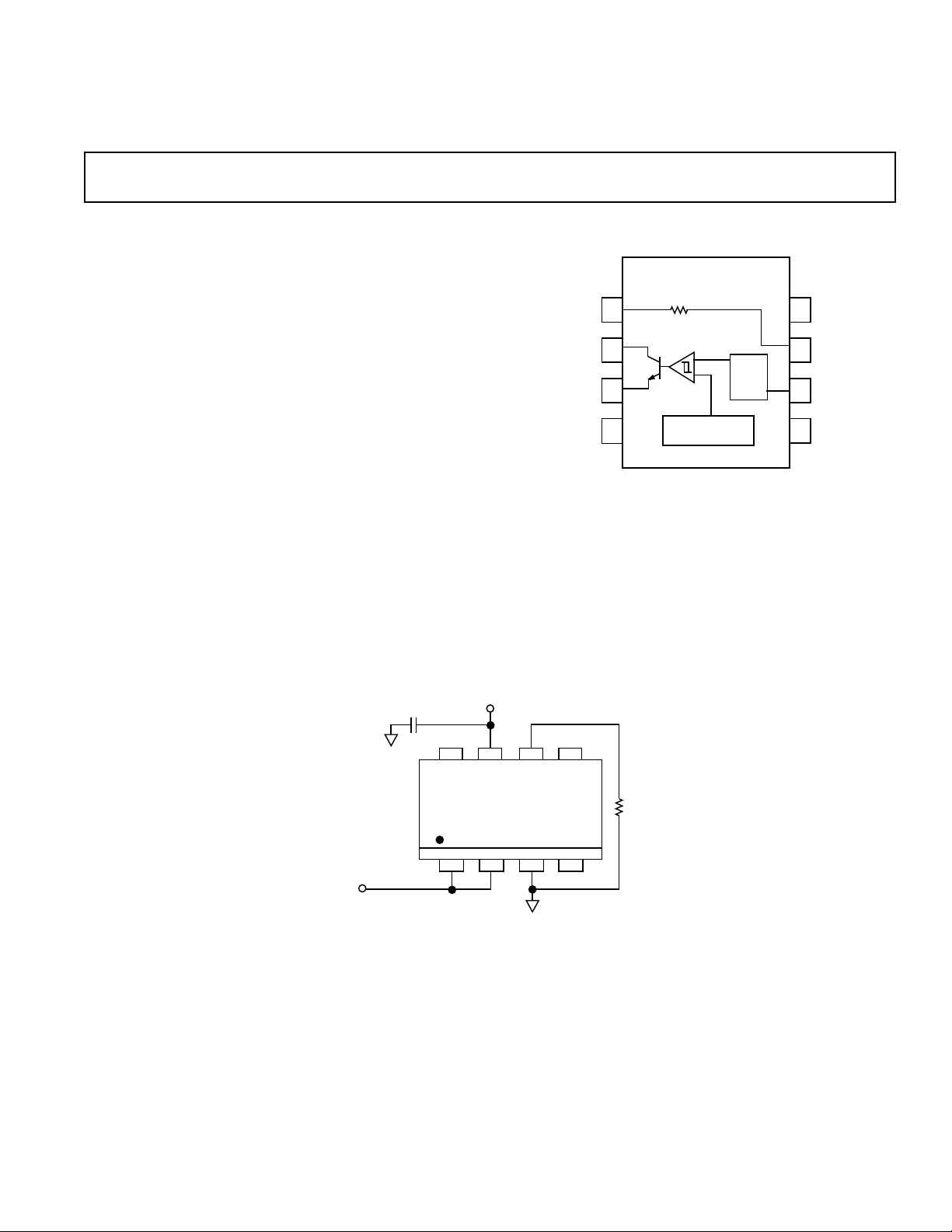
Thermostatic Switch
AD22105
FUNCTIONAL BLOCK DIAGRAM
AD22105
R
PULL–UP
OUT
GND
NC
1
2
3
4
The AD22105 is designed to operate on a single power supply
voltage from +2.7 V to +7.0 V facilitating operation in battery
powered applications as well as in industrial control systems.
Because of low power dissipation (230 µW @ 3.3 V), selfheating errors are minimized and battery life is maximized.
An optional internal 200 kΩ pull-up resistor is included to
facilitate driving light loads such as CMOS inputs.
Alternatively, a low power LED indicator may be driven directly.
200kΩ
TEMPERATURE
SENSOR
SET–
POINT
8
NC
V
S
7
R
6
SET
NC
5
+2.7V TO +7.0V
8
12
OUT
Figure 1. Typical Application Circuit
REV. 0
Information furnished by Analog Devices is believed to be accurate and
reliable. However, no responsibility is assumed by Analog Devices for its
use, nor for any infringements of patents or other rights of third parties
which may result from its use. No license is granted by implication or
otherwise under any patent or patent rights of Analog Devices.
65
7
AD22105
TOP VIEW
4
3
One Technology Way, P.O. Box 9106, Norwood, MA 02062-9106, U.S.A.
Tel: 617/329-4700 Fax: 617/326-8703
R
SET
© Analog Devices, Inc., 1996
Page 2
AD22105–SPECIFICATIONS
(VS = 3.3 V, TA = +258C, R
= internal 200 kV, unless otherwise noted)
LOAD
Parameter Symbol Conditions Min Typ Max Units
TEMPERATURE ACCURACY
Ambient Setpoint Accuracy ACC ±0.5 ±2.0 °C
Temperature Setpoint Accuracy ACC
T
Power Supply Rejection PSR +2.7 V1 < V
–40°C ≤ TA ≤ +125°C ±3.0 °C
< +7.0 V ±0.05 ±0.15 °C/V
S
HYSTERESIS
Hysteresis Value HYS 4.1 °C
OPEN COLLECTOR OUTPUT
Output Low Voltage V
OL
I
= 5 mA 250 400 mV
SINK
POWER SUPPLY
Supply Range V
Supply Current, Output “LOW” IS
Supply Current, Output “HIGH” IS
INTERNAL PULL-UP RESISTOR R
TURN-ON SETTLING TIME t
NOTES
1
The AD22105 will operate at voltages as low as +2.2 V.
Specifications subject to change without notice.
- kΩ
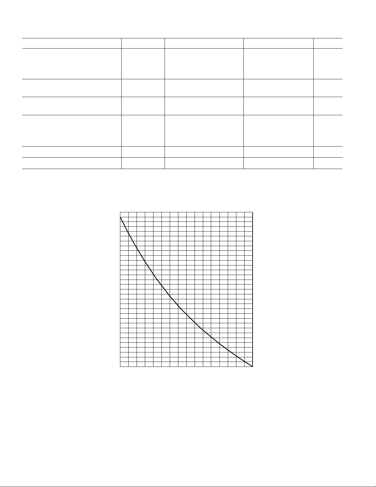
R
80
75
70
65
60
55
50
45
40
SET
35
30
25
20
15
10
5
0
–50 150–25
ON
S
ON
OFF
PULL-UP
39MΩ °C
= ––––––––––––——— – 90.3kΩ
R
SET
T
(°C) + 281.6 °C
SET
25 50 75 100 125
0
SET POINT TEMPERATURE – °C
+2.7 +7.0 V
120 µA
90 µA
140 200 260 kΩ
5 µs
Figure 2. Setpoint Resistor Values
REV. 0–2–
Page 3

AD22105
1
2
3
4
8
7
6
5
NC = NO CONNECT
AD22105
R
PULL-UP
NC
R
SET
V
S
NC
OUT
GND
NC
TOP VIEW
(Not to Scale)
ABSOLUTE MAXIMUM RATINGS*
PIN CONFIGURATION
Maximum Supply Voltage . . . . . . . . . . . . . . . . . . . . . . . +11 V
Maximum Output Voltage (Pin 2) . . . . . . . . . . . . . . . . +11 V
Maximum Output Current (Pin 2) . . . . . . . . . . . . . . . 10 mA
Operating Temperature Range . . . . . . . . . . –50°C to +150°C
Dice Junction Temperature . . . . . . . . . . . . . . . . . . . . +160°C
Storage Temperature Range . . . . . . . . . . . . –65°C to +160°C
Lead Temperature (Soldering, 10 sec) . . . . . . . . . . . +300°C
*Stresses above those listed under “Absolute Maximum Ratings” may cause
permanent damage to the device. This is a stress rating only and functional
operation of the device at these or any other conditions above those listed in the
operational sections of this specification is not implied. Exposure to absolute
maximum rating conditions for extended periods may affect device reliability.
PIN DESCRIPTION
Pin No. Description
ORDERING GUIDE
Package Package
Model Description Option
AD22105AR 8-Lead SOIC SO-8
AD22105AR-REEL7 8-Lead SOIC SO-8
1R
2 OUT
3 GND
4 No Connection
5 No Connection
6R
7V
Internal 200 kΩ (Optional)
PULL-UP,
, Temperature Setpoint Resistor
SET
S
8 No Connection
CAUTION
ESD (electrostatic discharge) sensitive device. Electrostatic charges as high as 4000 V readily
accumulate on the human body and test equipment and can discharge without detection.
Although the AD22105 features proprietary ESD protection circuitry, permanent damage may
occur on devices subjected to high energy electrostatic discharges. Therefore, proper ESD
precautions are recommended to avoid performance degradation or loss of functionality.
WARNING!
ESD SENSITIVE DEVICE
REV. 0 –3–
Page 4

AD22105–Typical Performance Characteristics
4
3
2
1
0
ERROR – °C
–1
–2
–3
–4
–50 150–25 0 25 50 75 100 125
GUARANTEED LIMIT (+)
GUARANTEED LIMIT (–)
TEMPERATURE – °C
Figure 3. Error vs. Setpoint
±
0.1
±
0.3
±
0.5
±
ERROR – °C/%
0.7
±
0.9
±
1.1
–50 150–25 0 25 50 75 100 125
TEMPERATURE – °C
4.4
4.2
4.0
3.8
HYSTERESIS – °C
3.6
3.4
3.2
–50 150–25 0 25 50 75 100 125
TEMPERATURE – °C
Figure 6. Hysteresis vs. Setpoint
2.0
1.5
1.0
0.5
0.0
ERROR – °C
–0.5
–1.0
–1.5
–2.0
3745 6
+125°C
+25°C
–40°C
V
S
Figure 4. Setpoint Error Due to R
90
80
70
– µA
S
I
60
50
40
–50 150–25 0 25 50 75 100 125
VS = 7V
VS = 5V
VS = 3V
TEMPERATURE – °C
Tolerance
SET
Figure 5. Supply Current vs. Temperature (V
= HIGH)
OUT
Figure 7. Setpoint Error vs. Supply Voltage
120
VS = 7V
110
100
90
– µA
S
I
80
70
60
–50 150–25 0 25 50 75 100 125
VS = 5V
VS = 3V
TEMPERATURE – °C
Figure 8. Supply Current vs. Temperature (V
= LOW)
OUT
–4–
REV. 0
Page 5

AD22105
0.4
0.3
0.2
OUT
V
0.1
0.0
Figure 9. V
16
14
12
10
– sec
τ
8
6
4
2
0 1200400 800
10µA 10mA1mA100µA1µA
OUT
I
OUT
vs. I
OUT
FLOW RATE – CFM
TA = +150°C
TA = +25°C
(V
OUT
TA = –40°C
= LOW)
250
200
150
– °C/W
JA
θ
100
50
0 1200
400 800
FLOW RATE – CFM
Figure 11. Thermal Resistance vs. Flow Rate
100
90
80
70
60
50
40
% OF FINAL VALUE
30
20
10
0
06010 20 30 40 50
MOVING AIR
(1200 CFM)
STILL AIR
TIME – sec
Figure 10. Thermal Response vs. Flow Rate
Figure 12. Thermal Response Time
REV. 0 –5–
Page 6

AD22105
PRODUCT DESCRIPTION
The AD22105 is a single supply semiconductor thermostat
switch that utilizes a unique circuit architecture to realize the
combined functions of a temperature sensor, setpoint comparator,
and output stage all in one integrated circuit. By using one
external resistor, the AD22105 can be programmed to switch at
any temperature selected by the system designer in the range of
–40°C to +150°C. The internal comparator is designed to switch
very accurately as the ambient temperature rises past the
setpoint temperature. When the ambient temperature falls, the
comparator relaxes its output at a somewhat lower temperature
than that at which it originally switched. The difference between
the “switch” and “unswitch” temperatures, known as the hysteresis,
is designed to be nominally 4°C.
THE SETPOINT RESISTOR
The setpoint resistor is determined by the equation:
=
39 MΩ°C
(°C)+281.6°C
T
SET
–90.3kΩ
Eq. 1
R
SET
The setpoint resistor should be connected directly between the
R
pin (Pin 6) and the GND pin (Pin 3). If a ground plane is
SET
used, the resistor may be connected directly to this plane at the
closest available point.
The setpoint resistor, R
, can be of nearly any resistor type,
SET
but its initial tolerance and thermal drift will affect the accuracy
of the programmed switching temperature. For most applications,
a 1% metal-film resistor will provide the best tradeoff between
cost and accuracy. Calculations for computing an error budget
can be found in the section “Effect of Resistor Tolerance and
Thermal Drift on Setpoint Accuracy.”
Once R
has been calculated, it may be found that the calcu-
SET
lated value does not agree with readily available standard
resistors of the chosen tolerance. In order to achieve an R
SET
value as close as possible to the calculated value, a compound
resistor can be constructed by connecting two resistors in series
or in parallel. To conserve cost, one moderately precise resistor
and one lower precision resistor can be combined. If the moderately precise resistor provides most of the necessary resistance,
the lower precision resistor can provide a fine adjustment. Consider an example where the closest standard 1% resistor has only
90% of the value required for R
. If a 5% series resistor is
SET
used for the remainder, then its tolerance only adds 5% of 10%
or 0.5% additional error to the combination. Likewise, the 1%
resistor only contributes 90% of 1% or 0.9% error to the combination. These two contributions are additive resulting in a total
compound resistor tolerance of 1.4%.
EFFECT OF RESISTOR TOLERANCE AND THERMAL DRIFT ON SETPOINT ACCURACY
Figure 3 shows the typical accuracy error in setpoint temperature
as a function of the programmed setpoint temperature. This
curve assumes an ideal resistor for R
. The graph of Figure 4
SET
may be used to calculate additional setpoint error as a function
of resistor tolerance. Note that this curve shows additional error
beyond the initial accuracy error of the part and should be
added to the value found in the specifications table. For example,
consider using the AD22105 programmed to switch at +125°C.
Figure 4 indicates that at +125°C, the additional error is
approximately –0.2°C/% of R
. If a 1% resistor (of exactly
SET
correct nominal value) is chosen, then the additional error could
be –0.2°C/% × 1% or –0.2°C. If the closest standard resistor
value is 0.6% away from the calculated value, then the total
error would be 0.6% for the nominal value and 1% for the
tolerance or (1.006) × (1.10) or 1.01606 (about 1.6%). This
could lead to an additional setpoint error as high as 0.32°C.
For additional accuracy considerations, the thermal drift of the
setpoint resistor can be taken into account. For example, consider that the drift of the metal film resistor is 100 ppm/°C.
Since this drift is usually referred to +25°C, the setpoint resistor
can be in error by an additional 100 ppm/°C × (125°C – 25°C) or
1%. Using a setpoint temperature of 125°C as discussed above,
this error source would add an additional –0.2°C (for positive drift)
making the overall setpoint error potentially –0.52°C higher than
the original accuracy error.
Initial tolerance and thermal drift effects of the setpoint resistor
can be combined and calculated by using the following
equation:
R
MAX
= R
×(1 +ε)× 1+TC×(T
NOM
()
SET
–25°C)
where:
R
R
is the worst case value that the setpoint resistor can be at
MAX
T
,
SET
is the standard resistor with a value closest to the desired
NOM
R
,
SET
ε is the 25°C tolerance of the chosen resistor (usually 1%,
5%, or 10%),
T
T
Once calculated, R
is the temperature coefficient of the available resistor,
C
is the desired setpoint temperature.
SET
may be compared to the desired R
MAX
SET
from Equation 1. Continuing the example from above, the
required value of R
SET
at a T
of 125°C is 5.566 kΩ. If the
SET
nearest standard resistor value is 5.600 kΩ, then its worst case
maximum value at 125°C could be 5.713 kΩ. Again this is
+2.6% higher than R
leading to a total additional error of
SET
–0.52°C beyond that given by the specifications table.
THE HYSTERESIS AND SELF-HEATING
The actual value of the hysteresis generally has a minor
dependence on the programmed setpoint temperature as shown
in Figure 6. Furthermore, the hysteresis can be affected by selfheating if the device is driving a heavy load. For example, if the
device is driving a load of 5 mA at an output voltage (given by
Figure 9) of 250 mV, then the additional power dissipation
would be approximately 1.25 mW. With a θ
of 190°C/W in
JA
free air the internal die temperature could be 0.24°C higher
than ambient leading to an increase of 0.24°C in hysteresis. In
the presence of a heat sink or turbulent environment, the
additional hysteresis will be less.
REV. 0–6–
Page 7

AD22105
OUTPUT SECTION
The output of the AD22105 is the collector of an NPN transistor.
When the ambient temperature of the device exceeds the
programmed setpoint temperature, this transistor is activated
causing its collector to become a low impedance. A pull-up
resistor, such as the internal 200 kΩ provided, is needed to
observe a change in the output voltage. For versatility, the
optional pull-up resistor has not been permanently connected
to the output pin. Instead, this resistor is undedicated and
connects from Pin 7 (V
R
(R
a single connection should be made from Pin 1
PULL-UP
) to Pin 2 (OUT).
PULL-UP
) to Pin 1 (R
S
). In order to use
PULL-UP
The 200 kΩ pull-up resistor can drive CMOS loads since
essentially no static current is required at these inputs. When
driving “LS” and other bipolar family logic inputs a parallel
resistor may be necessary to supply the 20 µA–50 µA I
(High
IH
Level Input Current) specified for such devices. To determine
the current required, the appropriate manufacturer’s data sheet
should be consulted. When the output is switched, indicating an
over temperature condition, the output is capable of pulling
down with 10 mA at a voltage of about 375 mV. This allows for
a fan out of 2 with standard bipolar logic and 20 with “LS”
family logic.
Low power indicator LEDs (up to 10 mA) can be driven
directly from the output pin of the AD22105. In most cases a
small series resistor (usually of several hundred ohms) will be
required to limit the current to the LED and the output
transistor of the AD22105.
MOUNTING CONSIDERATIONS
If the AD22105 is thermally attached and properly protected, it
can be used in any measuring situation where the maximum
range of temperatures encountered is between –40°C and
+150°C. Because plastic IC packaging technology is employed,
excessive mechanical stress must be avoided when fastening the
device with a clamp or screw-on heat tab. Thermally conductive
epoxy or glue is recommended for typical mounting conditions.
In wet or corrosive environments, an electrically isolated metal
or ceramic well should be used to protect the AD22105.
THERMAL ENVIRONMENT EFFECTS
The thermal environment in which the AD22105 is used
determines two performance traits: the effect of self-heating on
accuracy and the response time of the sensor to rapid changes in
temperature. In the first case, a rise in the IC junction temperature above the ambient temperature is a function of two variables:
the power consumption of the AD22105 and the thermal
resistance between the chip and the ambient environment, θ
.
JA
Self-heating error can be derived by multiplying the power
dissipation by θ
Because errors of this type can vary widely for
JA.
surroundings with different heat sinking capacities, it is
necessary to specify θ
under several conditions. Table I shows
JA
how the magnitude of self-heating error varies relative to the
environment. A typical part will dissipate about 230 µW at
room temperature with a 3.3 V supply and negligible output
loading. In still air, without a “heat sink,” Table I indicates a
of 190°C/W, which yields a temperature rise of 0.04°C.
θ
JA
Thermal rise of the die will be considerably less in an environment of turbulent or constant moving air or if the device is in
direct physical contact with a solid (or liquid) body.
Response of the AD22105 internal die temperature to abrupt
changes in ambient temperatures can be modeled by a single
time constant exponential function. Figure 11 shows typical
response plots for moving and still air. The time constant, τ
(time to reach 63.2% of the final value), is dependent on θ
JA
and
the thermal capacities of the chip and the package. Table I lists
the effective τ for moving and still air. Copper printed circuit
board connections were neglected in the analysis; however, they
will sink or conduct heat directly through the AD22105’s solder
plated copper leads. When faster response is required, a thermally conductive grease or glue between the AD22105 and the
surface temperature being measured should be used.
Table I. Thermal Resistance (SO-8)
Medium uJA (8C/Watt) t (sec)*
Moving Air** 100 3.5
Without Heat Sink
Still Air 190 15
Without Heat Sink
NOTES
**The time constant is defined as the time to reach 63.2% of the final tempera-
ture change.
**1200 CFM.
USING THE AD22105 AS A COOLING SETPOINT DETECTOR
The AD22105 can be used to detect transitions from higher
temperatures to lower temperatures by programming the
setpoint temperature 4°C greater than the desired trip point
temperature. The 4°C is necessary to compensate for the
nominal hysteresis value designed into the device. A more
precise value of the hysteresis can be obtained from Figure 6. In
this mode, the logic state of the output will indicate a HIGH for
under temperature conditions. The total device error will be
slightly greater than the specification value due to uncertainty in
hysteresis.
APPLICATION HINTS
EMI Suppression
Noisy environments may couple electromagnetic energy into the
node causing the AD22105 to falsely trip or untrip. Noise
R
SET
sources, which typically come from fast rising edges, can be
coupled into the device capacitively. Furthermore, if the output
signal is brought close the R
OUT pin to the R
pin potentially causing oscillation. Stray
SET
pin, energy can couple from the
SET
capacitance can come from several places such as, IC sockets,
multiconductor cables, and printed circuit board traces. In some
cases, it can be corrected by constructing a Faraday shield
around the R
pin, for example, by using a shielded cable with
SET
the shield grounded. However, for best performance, cables
should be avoided and the AD22105 should be soldered directly
to a printed circuit board whenever possible. Figure 13 shows a
sample printed circuit board layout with low inter-pin capacitance and Faraday shielding. If stray capacitance is unavoidable,
and interference or oscillation occurs, a low impedance capacitor should be connected from the R
pin to the GND pin.
SET
This capacitor must be considerably larger than the estimated
stray capacitance. Typically several hundred picofarads will correct the problem.
REV. 0 –7–
Page 8

AD22105
Leakage at the R
Leakage currents at the R
SET
Pin
pin, such as those generated from a
SET
moist environment or printed circuit board contamination, can
have an adverse effect on the programmed setpoint temperature
of the AD22105. Depending on its source, leakage current can
flow into or out of the R
pin. Consequently, the actual
SET
setpoint temperature could be higher or lower than the intended
setpoint temperature by about 1°C for each 75 nA of leakage.
With a 5 V power supply, an isolation resistance of 100 MΩ
would create 50 nA of leakage current giving a setpoint
temperature error of about 0.7°C (the R
potential). A guard ring can be placed around the R
pin is near ground
SET
node to
SET
protect against leakage from the power supply pin (as shown in
Figure 13).
V
S
C1
R
SET
0.1574 (4.00)
0.1497 (3.80)
PIN 1
0.0098 (0.25)
0.0040 (0.10)
SEATING
PLANE
OUTLINE DIMENSIONS
Dimensions shown in inches and (mm).
8-Lead SOIC
(SO-8)
0.1968 (5.00)
0.1890 (4.80)
8
5
0.2440 (6.20)
41
0.2284 (5.80)
0.0500
(1.27)
BSC
0.0688 (1.75)
0.0532 (1.35)
0.0192 (0.49)
0.0138 (0.35)
0.0098 (0.25)
0.0075 (0.19)
0.0196 (0.50)
0.0099 (0.25)
8°
0°
0.0500 (1.27)
0.0160 (0.41)
C2099–6–1/96
x 45°
PIN 1
OUT
Figure 13. Suggested PCB Layout
GND
PRINTED IN U.S.A.
REV. 0–8–
 Loading...