

Page 1
Single-Supply Sensor
a
FEATURES
Gain of ⴛ20. Alterable from ⴛ1 to ⴛ160
Input CMR from Below Ground to 6ⴛ (VS – 1 V)
Output Span 20 mV to (V
1-, 2-, 3-Pole Low-Pass Filtering Available
Accurate Midscale Offset Capability
Differential Input Resistance 400 k⍀
Drives 1 k⍀ Load to +4 V Using V
Supply Voltage: +3.0 V to +36 V
Transient Spike Protection and RFI Filters Included
Peak Input Voltage (40 ms): 60 V
Reversed Supply Protection: –34 V
Operating Temperature Range: –40ⴗC to +125ⴗC
APPLICATIONS
Current Sensing
Motor Control
Interface for Pressure Transducers, Position Indicators,
Strain Gages, and Other Low Level Signal Sources
Accelerometers
– 0.2) V
S
= +5 V
S
Interface Amplifier
FUNCTIONAL BLOCK DIAGRAM
+V
IN+
IN–
AD22057
A1
S
OFS A1
A2
AD22057
A2
OUT
GND
GENERAL DESCRIPTION
The AD22057 is a single-supply difference amplifier for amplifying and low-pass filtering small differential voltages (typically
100 mV FS at a gain of 40) from sources having a large commonmode voltage.
Supply voltages from +3.0 V to +36 V can be used. The input
common-mode range extends from below ground to +24V using
+V
(CAR BATTERY)
S
CMOS DRIVER
CHASSIS
SOLENOID
LOAD
100mV
POWER
DARLINGTON
SINGLE-POLE LOW-PASS FILTERING, GAIN: 40
Figure 1. Typical Application Circuit for a Current Sensor Interface
a +5 V supply with excellent rejection of this common-mode
voltage. This is achieved by the use of a special resistive attenuator at the input, laser trimmed to a very high differential balance.
Provisions are included for optional low-pass filtering and gain
adjustment. An accurate midscale offset feature allows bipolar
signals to be amplified.
+5V
ANALOG OUTPUT
4V PER AMP
AD22057
C
200kV
CORNER FREQUENCY
= 0.796Hz-mF
ANALOG GROUND
REV. A
Information furnished by Analog Devices is believed to be accurate and
reliable. However, no responsibility is assumed by Analog Devices for its
use, nor for any infringements of patents or other rights of third parties
which may result from its use. No license is granted by implication or
otherwise under any patent or patent rights of Analog Devices.
One Technology Way, P.O. Box 9106, Norwood, MA 02062-9106, U.S.A.
Tel: 781/329-4700 World Wide Web Site: http://www.analog.com
Fax: 781/326-8703 © Analog Devices, Inc., 1999
Page 2
AD22057–SPECIFICATIONS
(TA = +25ⴗC, VS = +5 V, VCM = 0, RL = 10 k⍀ unless otherwise noted)
Parameter Comments Test Conditions Min Typ Max Units
INPUTS (PINS 1 AND 8)
+CMR Positive Common-Mode Range TA = T
CMR Negative Common-Mode Range T
CMRR
LF
CMRR
HF
R
INCM
R
MATCH
R
INDIFF
PREAMPLIFIER
G
CL
V
O
R
O
OUTPUT BUFFER
G
CL
V
O
R
O
OVERALL SYSTEM
G Gain
V
OS
Common-Mode Rejection Ratio f ≤ 10 Hz 80 90 dB
Common-Mode Rejection Ratio f = 1 kHz 80 90 dB
Common-Mode Input Resistance Pin 1 or Pin 8 to Pin 2 180 240 300 kΩ
Matching of Resistances ±0.5 %
Differential Input Resistance Pin 1 to Pin 8 280 400 kΩ
Closed-Loop Gain
Output Voltage Range (Pin 3) +0.01 +4.8 V
Output Resistance
Closed-Loop Gain
Output Voltage Range
1
2
1
3
R
Output Resistance (Pin 5) VO ≥ 0.1 V dc 2.0 Ω
1
Gain Drift T
Input Offset Voltage
4
VO ≥ 0.1 V dc 19.9 20.0 20.1 V/V
Offset Drift T
= T
A
LOAD
= T
A
= T
A
to T
MIN
MIN
MAX
to +85°C –1.0 V
+24 V
9.7 10.0 10.3 V/V
97 100 103 kΩ
≥ 10 kΩ 1.94 2.0 2.06 V/V
+0.02 +4.8 V
MIN
to T
MAX
–62.5 +62.5 ppm/°C
–1 0.03 1 mV
MIN
to T
MAX
–12.5 +12.5 µV/°C
OFS Midscale Offset (Pin 7) Scaling 0.49 0.50 0.51 V/V
Input Resistance Pin 7 to Pin 2 2.5 3.0 kΩ
I
OSC
BW
–3 dB
SR Slew Rate 0.2 V/µs
N
SD
PSR Power Supply Rejection V
V
OS
Short-Circuit Output Current 7 11 25 mA
T
= T
A
MIN
to T
MAX
527mA
–3 dB Bandwidth VO = +1 V dc 20 30 kHz
Noise Spectral Density
Input Offset Voltage
4
4
f = 100 Hz to 10 kHz 0.2 µV/√Hz
= 5 V, VO = 1 V to 4.2 V
S
V
= 24 V, VO = 1 V to 22 V
S
= T
T
A
MIN
to T
MAX
20.0 µV/V
G Gain 0.05 %/V
POWER SUPPLY
V
S
I
S
Operating Range TA = T
Quiescent Supply Range
5
TA = +25°C, VS = +5 V 200 500 µA
MIN
to T
MAX
3536V
TEMPERATURE RANGE
T
OP
Operating Temperature Range –40 +125 °C
PACKAGE Plastic Mini-DIP (N-8) AD22057N
Plastic SOIC (SO-8) AD22057R
NOTES
1
Specified for default mode i.e., with no external components. The overall gain is trimmed to ±0.5% while the individual gains of A1 and A2 may be subject to a
maximum ±3% tolerance. Note that the actual gain in a particular application can be modified by the use of external resistor networks.
2
The actual output resistance of A1 is only a few ohms, but access to this output, via Pin 3, is always through a 100 kΩ resistor, which is trimmed to ±3%.
3
For VCM ≤ 20 V. For VCM > 20 V, VOL ⯝ 1 mV/V × VCM.
4
Referred to the input (Pins 1 and 8).
5
With VDM = 0 V. Differential mode signals are referred to as VDM, while VCM refers to common-mode voltages.
Specifications subject to change without notice.
ORDERING GUIDE
Model Temperature Range Package Descriptions Package Options
AD22057N –40°C to +125°C Plastic DIP N-8
AD22057R –40°C to +125°C Plastic SOIC SO-8
AD22057R-Reel –40°C to +125°C Tape and Reel SO-8*
*Quantities must be in increments of 2,500 pieces each.
–2–
REV. A
Page 3
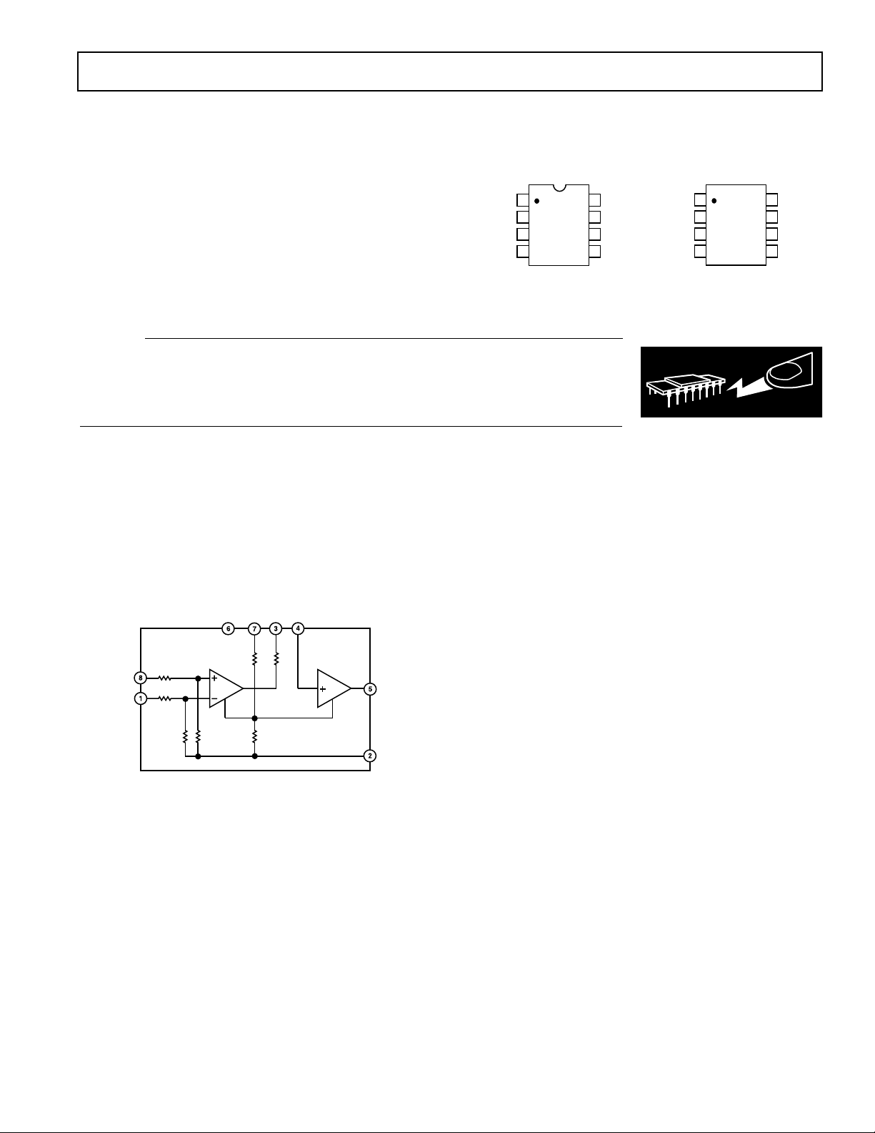
AD22057
WARNING!
ESD SENSITIVE DEVICE
ABSOLUTE MAXIMUM RATINGS*
PIN CONFIGURATIONS
Supply Voltage . . . . . . . . . . . . . . . . . . . . . . . . +3.0 V to +36 V
Peak Input Voltage (40 ms) . . . . . . . . . . . . . . . . . . . . . . +60 V
(Pin 7 to Pin 2) . . . . . . . . . . . . . . . . . . . . . . . . . . . .+20 V
V
OFS
Plastic Mini-DIP Package
(N-8)
Reversed Supply Voltage Protection . . . . . . . . . . . . . . . –34 V
Operating Temperature . . . . . . . . . . . . . . . . –40°C to +125°C
Storage Temperature . . . . . . . . . . . . . . . . . . –65°C to +150°C
Output Short Circuit Duration . . . . . . . . . . . . . . . . Indefinite
Lead Temperature Range (Soldering 60 sec) . . . . . . . . +300°C
*Stresses above those listed under Absolute Maximum Ratings may cause perma-
nent damage to the device. This is a stress rating only; the functional operation of
the device at these or any other conditions above those indicated in the operational
sections of this specification is not implied. Exposure to absolute maximum rating
conditions for extended periods may affect device reliability.
–IN
GND
A1
1
2
AD22057
TOP VIEW
3
(Not to Scale)
4
8
+IN
OFFSET
7
+V
6
OUTA2
5
S
CAUTION
ESD (electrostatic discharge) sensitive device. Electrostatic charges as high as 4000 V readily
accumulate on the human body and test equipment and can discharge without detection.
Although the AD22057 features proprietary ESD protection circuitry, permanent damage may
occur on devices subjected to high energy electrostatic discharges. Therefore, proper ESD
precautions are recommended to avoid performance degradation or loss of functionality.
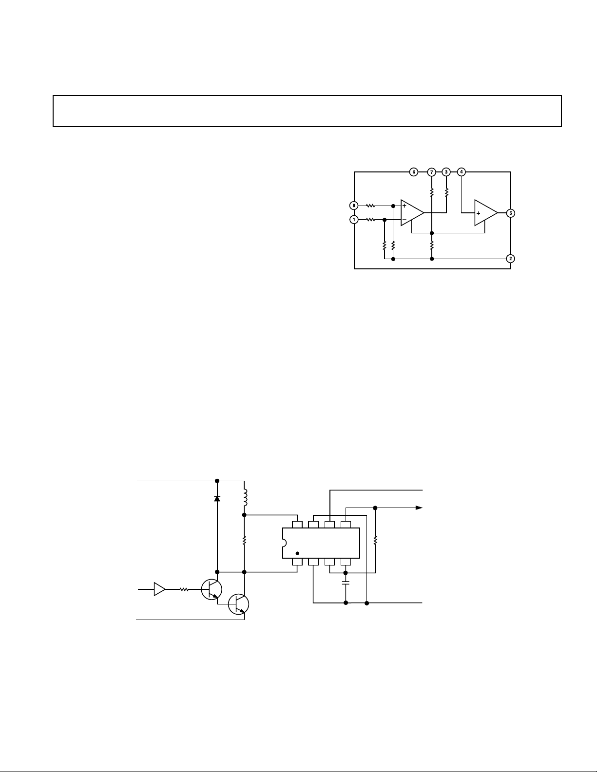
PRODUCT DESCRIPTION
The AD22057 is a single-supply difference amplifier consisting
of a precision balanced attenuator, a very low drift preamplifier
and an output buffer amplifier (A1 and A2, respectively, in
Figure 2). It has been designed so that small differential signals (V
in the presence of large common-mode voltages (V
in Figure 3) can be accurately amplified and filtered
DM
) without
CM
the use of any other active components.
+V
AD22057
S
OFS A1
A2
offset to an optional voltage of one half of that supplied to Pin 7;
in many cases this offset would be +VS/2 by tying Pin 7 to +V
(Pin 6), permitting the conditioning and processing of bipolar
signals (see Strain Gage Interface section).
The output buffer A2 has a gain of ×2, setting the precalibrated,
overall gain of the AD22057, with no external components, to
×20. (This gain is easily user-configurable—see Altering the
Gain section for details.)
The dynamic properties of the AD22057 are optimized for interfacing to transducers; in particular, current sensing shunt
resistors. Its rejection of large, high frequency, common-mode
signals makes it superior to that of many alternative approaches.
IN+
IN–
A1
A2
OUT
This is due to the very careful design of the input attenuator and
the close integration of this highly balanced, high impedance
system with the preamplifier.
Plastic SOIC Package
(SO-8)
–IN
GND
A1
A2
1
2
AD22057
TOP VIEW
3
(Not to Scale)
4
8
+IN
7
OFFSET
6
+V
OUT
5
S
S
GND
Figure 2. Simplified Schematic
The resistive attenuator network is situated at the input to the
AD22057 (Pins 1 and 8), allowing the common-mode voltage at
Pins 1 and 8 to be six times greater than that which can be tolerated by the actual input to A1. As a result, the input commonmode range extends to 6× (V
– 1 V).
S
Two small filter capacitors (not shown in Figure 2) have been
included at the inputs of A1 to minimize the effects of any spurious RF signals present in the signal.
Internal feedback around A1 sets the closed-loop gain of the
preamplifier to ×10 from the input pins; the output of A1 is
connected to Pin 3 via a 100 kΩ resistor, which is trimmed to
±3% (R12 in Figure 2) to facilitate the low-pass filtering of the
signal of interest (see Low-Pass Filtering section). The inclusion
of an additional resistive network allows the output of A1 to be
REV. A
–3–
APPLICATIONS
The AD22057 can be used wherever a high gain, single-supply
differencing amplifier is required, and where a finite input resistance (240 kΩ to ground, 400 kΩ between differential inputs)
can be tolerated. In particular, the ability to handle a commonmode input considerably larger than the supply voltage is frequently of value.
Also, the output can run down to within 20 mV of ground,
provided it is not called on to sink any load current. Finally, the
output can be offset to half of a full-scale reference voltage (with
a tolerance of ±2%) to allow a bipolar input signal.
ALTERING THE GAIN
The gain of the preamplifier, from the attenuator input (Pins 1
and 8) to its output at Pin 3, is ×10 and that of the output
buffer, from Pin 4 to Pin 5, is ×2, thus making the overall default gain ×20. The overall gain is accurately trimmed (to within
±0.5%). In some cases, it may be desirable to provide for some
variation in the gain; for example, in absorbing the scaling error
of a transducer.
Page 4

AD22057
Figure 3 shows a general method for trimming the gain, either
upward or downward, by an amount dependent on the resistor,
R. The gain range, expressed as a percentage of the overall gain,
is given by (10 MΩ/R)%. Thus, the adjustment range would be
±2% for R = 5 MΩ; ± 10% for R = 1 MΩ, etc.
ANALOG
OUTPUT
DM
CM
+IN OFS +VSOUT
AD22057
–IN GND A1 A2
R
(SEE TEXT)
= COMMOM-MODE VOLTAGE
6GAIN ADJUST
20kV MIN
ANALOG
COMMON
V
V
V
= DIFFERENTIAL VOLTAGE, V
Figure 3. Altering Gain to Accommodate Transducer
Scaling Error
In addition to the method above, another method may be used
to vary the gain. Many applications will call for a gain higher
than ×20, and some require a lower gain. Both of these situations are readily accommodated by the addition of one external
resistor, plus an optional potentiometer if gain adjustment is
required (for example, to absorb a calibration error in a transducer).
Decreasing the Gain. See Figure 4. Since the output of the
preamplifier has an output resistance of 100 kΩ, an external
resistor connected from Pin 4 to ground will precisely lower the
gain by a factor R/(100k+R). When configuring the AD22057
for any gain, the maximum input and the power supply being
used should be considered, since either the preamplifier or the
output buffer will reach its full-scale output (approximately
– 0.2 V) with large differential input voltages. The input of
V
S
the AD22057 is limited to no greater than (V – 0.2)/10, for
overall gains less than 10, since the preamplifier, with its fixed
gain of ×10, reaches its full scale output before the output
buffer. For V
= 5 V this is 0.48 V. For gains greater than 10,
S
however, the swing at the buffer output reaches its full-scale first
and limits the AD22057 input to (V
– 0.2)/G, where G is the
S
overall gain. Increasing the power supply voltage increases the
allowable maximum input. For V
= 5 V and a nominal gain of
S
20, the maximum input is 240 mV.
The overall bandwidth is unaffected by changes in gain using
this method, although there may be a small offset voltage due to
the imbalance in source resistances at the input to A2. In many
cases this can be ignored but, if desired, can be nulled by inserting a resistor in series with Pin 4 (at “Point X” in Figure 4) of
value 100 kΩ minus the parallel sum of R and 100 kΩ. For
example, with R = 100 kΩ (giving a total gain of ×10), the optional offset nulling resistor is 50 kΩ.
ANALOG
OUTPUT
AD22057
–IN
GND A1 A2
+V
OUT
S
POINT X
(SEE TEXT)
R
GAIN = –––––––––
R = 100k –––––––––
20R
R + 100kV
GAIN
20 – GAIN
ANALOG
COMMON
V
V
+IN OFS
DM
CM
Figure 4. Achieving Gains Less Than ×20
Increasing the Gain. The gain can be raised by connecting a
resistor from the output of the buffer amplifier (Pin 5) to its
noninverting input (Pin 4) as shown in Figure 5. The gain is
now multiplied by the factor R/(R–100k); for example, it is
doubled for R = 200 kΩ. Overall gains of up to ×160 (R = 114 kΩ)
are readily achievable in this way. Note, however, that the accuracy of the gain becomes critically dependent on resistor value at
high gains. Also, the effective input offset voltage at Pins 1 and
8 (about six times the actual offset of A1) limits the part’s use in
very high gain, dc-coupled applications. The gain may be trimmed
by using a fixed and variable resistor in series (see, for example,
Figure 10).
ANALOG
OUTPUT
DM
CM
+IN OFS +VSOUT
AD22057
–IN
GND A1 A2
POINT X
(SEE TEXT)
V
V
GAIN = –––––––––
R
R = 100k –––––––––
20R
R – 100kV
GAIN
GAIN – 20
ANALOG
COMMON
Figure 5. Achieving Gains Greater Than ×20
Once again, a small offset voltage will arise from an imbalance
in source resistances and the finite bias currents inherently
present at the input of A2. In most applications this additional
offset error (about 130 µV at ×40) will be comparable with the
specified offset range and will therefore introduce negligible
skew. It may, however, be essentially eliminated by the addition
of a resistor in series with the parallel sum of R and 100 kΩ
(i.e., at “Point X” in Figure 5) so the total series resistance is
maintained at 100 kΩ. For example, at a gain of ×30, when
R = 300 kΩ and the parallel sum of R and 100 kΩ is 75 kΩ, the
padding resistor should be 25 kΩ. A 50 kΩ pot would provide
an offset range of about ±2.25 mV referred to the output, or
±75 µV referred to the attenuator input. A specific example is
shown in Figure 12.
LOW-PASS FILTERING
In many transducer applications it is necessary to filter the signal to remove spurious high frequency components, including
noise, or to extract the mean value of a fluctuating signal with a
peak-to-average ratio (PAR) greater than unity. For example, a
full wave rectified sinusoid has a PAR of 1.57, a raised cosine
has a PAR of 2 and a half wave sinusoid has a PAR of 3.14.
Signals having large spikes may have PARs of 10 or more.
When implementing a filter, the PAR should be considered so
the output of the AD22057 preamplifier (A1) does not clip
before A2 does, since this nonlinearity would be averaged and
appear as an error at the output. To avoid this error both amplifiers should be made to clip at the same time. This condition is
achieved when the PAR is no greater than the gain of the second
amplifier (2 for the default configuration). For example, if a
PAR of 5 is expected, the gain of A2 should be increased to 5.
Low-pass filters can be implemented in several ways using the
features provided by the AD22057. In the simplest case, a
single-pole filter (20 dB/decade) is formed when the output of
A1 is connected to the input of A2 via the internal 100 kΩ resistor by strapping Pins 3 and 4, and a capacitor added from this
node to ground, as shown in Figure 6. The dc gain remains ×20,
and the gain trim shown in Figure 3 may still be used. If a resistor is added across the capacitor to lower the gain, the corner
–4–
REV. A
Page 5

AD22057
(
)
frequency will increase; it should be calculated using the parallel
sum of the resistor and 100 kΩ.
ANALOG
OUTPUT
1
2pC 3 100kV
V
DM
V
CM
+IN OFS +VSOUT
AD22057
–IN
GND A1 A2
C
CORNER FREQUENCY =
THAT IS, 1.59Hz-mF
(C IS IN FARADS)
ANALOG
COMMON
Figure 6. Connections for Single-Pole, Low-Pass Filter
If the gain is raised using a resistor, as shown in Figure 5, the
corner frequency is lowered by the same factor as the gain is
raised. Thus, using a resistor of 200 kΩ (for which the gain
would be doubled) the corner frequency is now 0.796 Hz-µF,
(0.039 µF for a 20 Hz corner).
ANALOG
OUTPUT
DM
CM
+IN OFS +VSOUT
AD22057
–IN GND A1 A2
C
V
V
255kV
C
CORNER
FREQUENCY = 1Hz-mF
ANALOG
COMMON
Figure 7. Connections for Conveniently Scaled, Two-Pole,
Low-Pass Filter
A two-pole filter (with a roll-off of 40 dB/decade) can be implemented using the connections shown in Figure 7. This is a
Sallen & Key form based on a ×2 amplifier. It is useful to remember that a two-pole filter with a corner frequency f
one-pole filter with a corner at f
the frequency (f
40 Log(f
2/f1
2
/f1). The attenuation at that frequency is
2
). This is illustrated in Figure 8. Using the standard
have the same attenuation at
1
and a
2
resistor value shown, and equal capacitors (in Figure 7), the
corner frequency is conveniently scaled at 1 Hz-µF (0.05 µF for
a 20 Hz corner). A maximally flat response occurs when the
resistor is lowered to 196 kΩ and the scaling is then 1.145 HzµF. The output offset is raised by about 4 mV (equivalent to
200 µV at the input pins).
ATTENUATION
40LOG (f2/f1)
FREQUENCY
–20dB/DECADE
A 1-POLE FILTER, CORNER f1,
AND A 2-POLE FILTER, CORNER f
HAVE THE SAME ATTENUATION,
–40LOG (f
), AT FREQUENCY f
2/f1
f
f
–40dB/DECADE
,
2
2
/f
2
1
f2/f
Figure 8. Comparative Responses of One- and Two-Pole
Low-Pass Filters
REV. A
–5–
A three-pole filter (with roll-off 60 dB/decade) can be formed by
adding a passive RC network at the output forming a real pole.
A three-pole filter with a corner frequency f
attenuation a one-pole filter of corner f
3
/f1, where the attenuation is 30 Log (f3/f1) (see the graph in
√f
3
has the same
3
has at a frequency
1
Figure 9). Using equal capacitor values, and a resistor of
160 kΩ, the corner-frequency calibration remains 1 Hz-µF.
ATTENUATION
30LOG (f3/f1)
FREQUENCY
–20dB/DECADE –60dB/DECADE
A 1-POLE FILTER, CORNER f1,
AND A 3-POLE FILTER, CORNER f
HAVE THE SAME ATTENUATION,
–30LOG (f3/f1), AT FREQUENCY (f
f
1
,
3
3
/f
3
1)
f
3
3
(f
/f1)
3
Figure 9. Comparative Responses of One- and Three-Pole
Low-Pass Filters
CURRENT SENSOR INTERFACE
A typical automotive application making use of the large
common-mode range is shown in Figure 10.
+V
(BATTERY)
S
FLYBACK
DIODE
CMOS DRIVER
CHASSIS
100mV
SOLENOID
LOAD
+IN OFS +VSOUT
AD22057
–IN
GND A1 A2
POWER
DARLINGTON
ANALOG OUTPUT
4V PER AMP
191kV
20kV
CORNER FREQUENCY
= 0.796Hz-mF
C
(0.22mF FOR f = 3.6Hz)
ANALOG COMMON
+5V
65% SENSOR
CALIBRATION
Figure 10. Current Sensor Interface. Gain Is ×40, SinglePole Low-Pass Filtering
The current in a load, here shown as a solenoid, is controlled by
a power transistor that is either cut off or saturated by a pulse at
its base; the duty-cycle of the pulse determines the average
current. This current is sensed in a small resistor. The average differential voltage across this resistor is typically 100 mV,
although its peak value will be higher by an amount that
depends on the inductance of the load and the control frequency. The common-mode voltage, on the other hand, extends
from roughly 1 V above ground, when the transistor is saturated, to about 1.5 V above the battery voltage, when the transistor is cut off and the diode conducts.
If the maximum battery voltage spikes up to +20 V, the commonmode voltage at the input can be as high as 21.5 V. This can be
measured using even a +5 V supply for the AD22057.
Page 6

AD22057
To produce a full-scale output of +4 V, a gain ×40 is used, adjust-
able by ±5% to absorb the tolerance in the sense resistor. There is
sufficient headroom to allow at least a 10% overrange (to +4.4 V).
The roughly triangular voltage across the sense resistor is averaged by a single-pole low-pass filter, here set with a corner frequency of f
= 3.6 Hz, which provides about 30 dB of attenuation
C
at 100 Hz. A higher rate of attenuation can be obtained by a
two-pole filter having f
= 20 Hz, as shown in Figure 11. Al-
C
though this circuit uses two separate capacitors, the total capacitance is less than half that needed for the single-pole filter.
C
= 1Hz-mF
+5V
ANALOG
OUTPUT
= 20Hz)
C
ANALOG
COMMON
+VS (BATTERY)
FLYBACK
DIODE
CMOS DRIVER
CHASSIS
100mV
SOLENOID
LOAD
+IN OFS +VSOUT
AD22057
–IN
GND A1 A2
POWER
DARLINGTON
432kV
50kV
127kV
C
CORNER FREQUENCY
(0.05mF FOR f
Figure 11. Illustration of Two-Pole Low-Pass Filtering
STRAIN GAGE INTERFACE: MIDSCALE OFFSET FEATURE
The AD22057 can be used to interface a strain gage to a subsequent process where only a single supply voltage is available. In
this application, the midscale offset feature is valuable, since the
output of the bridge may have either polarity. Figure 12 shows
typical connections.
+V
S
ANALOG OUTPUT
R
L
10kV
ANALOG COMMON
R
R
R
+IN OFS +VSOUT
AD22057
–IN GND A1 A2
V
G
R
(SETS GAIN
TO 3 100)
100kV
V
NULL
OS
OPTIONAL
LP FILTER
125kV
Figure 12. Typical Connections for a Strain Gage Interface
Using the Offset Feature
The offset is obtained by connecting Pin 7 (OFS) to the supply
voltage. In this way, the output of the AD22057 is centered to
midway between the supply and ground. In many systems the
supply will also serve as the reference voltage for a subsequent
A/D converter. Alternatively, Pin 7 may be tied to the reference
voltage from an independent source. The AD22057 is trimmed
to guarantee an accuracy of ±2% on the 0.5 ratio between the
voltage on Pin 7 and the output.
An ac excitation of up to ±2 V can also be used because the
common-mode range of the AD22057 extends to –1 V. Assuming a full-scale bridge output (V
) of ±10 mV, a gain of ×100
G
might be used to provide an output of ±1V (a full-scale range
of +1.5 V to +3.5 V). This gain is achieved using the method
discussed in connection with Figure 5. Note that the gainsetting resistor does not affect the accuracy of the midscale
offset. (However, if the gain were lowered, using a resistor to
ground, this offset would no longer be accurate.) A V
nulling
OS
pot is included for illustrative purposes. One-, two- and threepole filtering can also be implemented, as discussed in the
Low-Pass Filtering section.
Using the Midscale Offset Feature
Figure 13 shows a more detailed schematic of the output amplifier A2. Because this is a single supply device, the output
stage has no pull-down transistor. Such a transistor would limit
the minimum output to several hundred millivolts above
ground. When using the AD22057 in unipolar mode (Pin 7
grounded), the resistors making up the feedback network also
act as a pull-down for the output stage.
+V
S
A2
OUT
95kV
10kV
20kV
20kV
GND
OFS
R
L
Figure 13. Detailed Schematic of Output Amplifier A2
If the output is called upon to source current (not sink), then it
can swing almost completely to ground (within 20 mV). However, if the offset pin is connected to some positive voltage
source, this source will “pull up” the output voltage, thereby
limiting the minimum output swing. With no external load the
minimum output voltage possible is V
/2. For example, if Pin
OFS
7 is connected to +5 V, the minimum output voltage is equal
to the offset voltage of 2.5 V. By adding an additional load, as
shown, the output swing toward ground can be extended.
The relationship is described by:
OUT
1
>
V
OFS
2
V
*This 20 kΩ resistor is internal to the AD22057 and can vary by ±30%.
where RL is an externally applied load resistor. However, R
R
L
RL+20kΩ*
L
cannot be made arbitrarily small since this would require excessive current from the output. The output current should be
limited to 5 mA total.
–6–
REV. A
Page 7

AD22057
10kV
+V
S
10kV
LOAD
AD22057
A2
R
LAG
C
LAG
R
L
C
L
0.01mF
1kV
10kV
+V
S
10kV
AD22057
A2
mPROCESSOR
A/D
IN
APPLICATION HINTS
Frequency Compensation
As are all closed-loop op amp circuits, the AD22057 is sensitive
to capacitive loading at its output. However, the AD22057 is
sensitive at higher output voltages due to nonlinear effects in
the rail-to-rail design of the buffer amplifier (A2). In this
amplifier the output stage gain increases with increasing output
voltage. This behavior does not affect dc parameters such as
gain accuracy or linearity; however, it can compromise ac stability. When operating from a power supply of 5 V or less (and,
therefore, V
< 5 V), the AD22057 can drive capacitive
OUT
loads up to 25 pF with no external components. When operating at higher supply voltages (which are associated with higher
output voltages) and/or driving larger capacitive loads, an external compensation network should be used. Figure 14 shows an
R-C “snubber” circuit loading the output of the AD22057.
This combination, in conjunction with the internal 20 kΩ resistance, forms a lag network. This network attenuates the openloop gain of the amplifier at higher frequencies. The ratio of
to the load seen by the AD22057 determines the high
R
LAG
frequency attenuation seen by the op amp. If R
1/20th of the total load resistance (≈20 kΩ储R
is made
LAG
), then 26 dB of
L
attenuation is obtained at higher frequencies. The capacitor
) is used to control the frequency of the compensation
(C
LAG
network. It should be set to form a 5 µs time constant with the
resistor (R
R
and C
LAG
). Table I shows the recommended values of
LAG
for various values of external load resistor RL.
LAG
Ten percent tolerance on these components is acceptable.
Alternatively, the signal may be taken from the midpoint of
R
LAG–CLAG
. This output is particularly useful when driving
CMOS analog-to-digital converters. For more information see
the section Driving Charged Redistributed A/D Converters.
Note that when implementing this network large signal response is compromised. This occurs because there is no active
pull-down and the lag capacitor must discharge through the
internal feedback resistor (20 kΩ) giving a fairly long-time
constant. For example if C
= 0.01 µF, the large signal
LAG
negative slew characteristic is a decaying exponential with a
time constant of ≈200 µs.
Table I. Compensation Components vs. External Load
Resistor
R
L
R
LAG
C
LAG
>100 kΩ 470 Ω 0.01 µF
> 50 kΩ 390 Ω 0.01 µF
> 20 kΩ 270 Ω 0.047 µF
> 10 kΩ 200 Ω 0.047 µF
> 5 kΩ 100 Ω 0.1 µF
> 2 kΩ 47 Ω 0.22 µF
Driving Charge Redistribution A/D Converters
When driving CMOS ADCs, such as those embedded in popular microcontrollers, the charge injection (∆Q) can cause a
significant deflection in the AD22057 output voltage. Though
generally of short duration, this deflection may persist until
after the sample period of the ADC has expired. It is due to the
relatively high open-loop output impedance of the AD22057.
The effect can be significantly reduced by including the same
R-C network recommended for improving stability (see Frequency Compensation section). The large capacitor in the lag
REV. A
network helps to absorb the additional charge, effectively lowering the high frequency output impedance of the AD22057. For
these applications the output signal should be taken from the
midpoint of the R
LAG–CLAG
combination as shown in Figure 15.
Since the perturbations from the analog-to-digital converter are
small, the output of the AD22057 will appear to be a low
impedance. The transient response will, therefore, have a
time constant governed by the product of the two lag components, C
LAG
× R
. For the values shown in Figure 15, this
LAG
time constant is programmed at approximately 10 µs. There-
fore, if samples are taken at several tens of microseconds or more,
there will be negligible “stacking up” of the charge injections.
Figure 14. Using an R-C Network for Compensation
Figure 15. Recommended Circuit for Driving CMOS A/D
Converters
UNDERSTANDING THE AD22057
Figure 16 shows the main elements of the AD22057. The signal
inputs at Pins 1 and 8 are first applied to dual resistive attenuators R1 through R4, whose purpose is to reduce the commonmode voltage at the input to the preamplifier. The attenuated
signal is then applied to a feedback amplifier based on the very
low drift op amp, A1. The differential voltage across the inputs
is accurately amplified in the presence of common-mode voltages of many times the supply voltage. The overall commonmode response is minimized by precise laser trimming of R3
and R4, giving the AD22057 a common-mode rejection ratio
(CMRR) of at least 80 dB (10,000:1).
The common-mode range of A1 extends from slightly below
ground to 1 V below +V
(at the minimum temperature of
S
–40°C). Since an attenuation ratio of about 6 is used, the input
common-mode range is –1 V to +24 V using a +5 V supply.
Small filter capacitors C1 and C2 are included to minimize the
effects of spurious RF signals at the inputs, which might cause
dc errors due to the rectification effects at the input to A1. At
high frequencies, even a small imbalance in these components
would seriously degrade the CMRR, so a special high frequency
trim is also carried out during manufacture.
–7–
Page 8

AD22057
A unique method of feedback around A1, provided by R9 and
R7, sets the closed-loop gain of the preamplifier to ×10 (from
the input pins). The feedback network is balanced by the inclusion of R6 and R8. The small value of R7 results in a more
practical value for R9 (which would have to be 2 MΩ if the
feedback were taken directly to the inputs of A1). R8 is not
directly connected to ground, but to an optional voltage of one
half that is applied to Pin 7 (OFS). It is trimmed to within close
tolerances through R10 and R11. This allows the output of A1
to be offset to midscale, typically +V
/2, by tying Pins 6 and 7
S
together. (For an example of the use of this feature, see Figure
12.) The gain is adjusted by the single resistor R5, which acts
only on the differential signal. More importantly, it also results
in much less feed forward of the common-mode signal to the
output of A1, which, being a single-supply circuit, has no means
of pulling this output down toward ground in those circumstances where the common-mode input is very positive while the
net differential signal is small. (The output of A1 is the collector
of a PNP transistor whose emitter is tied to +V
.) R16 is specifi-
S
cally included to alleviate this problem.
The output of the preamplifier is connected to Pin 3 via R12, a
100 kΩ resistor that is trimmed to within ±3%. The inclusion of
R12 allows a low-pass filter to be formed, with an accurate time
constant, by placing a capacitor from Pin 3 to ground. By separating the connections at Pins 3 and 4, a two-pole Sallen and
Key filter can be formed (see Low-Pass Filtering section) and
also provides a means for setting the overall gain to values other
than ×20 (see Altering the Gain section).
The output buffer has a gain of ×2, set by the feedback network
around op amp A2, formed by R15 and R13储R14. Note that this
gain is not trimmed to a precise value, but may have a tolerance
of ±3% (max). Only the overall gain of A1 and A2 is trimmed to
within ±0.5% by R5. As a consequence, the gain of A1 may be
in error by ±3% (max) as the trim to R5 absorbs the initial error
in the gain of A2. In most applications Pins 3 and 4 are simply
tied together, but the output buffer can be used independently if
desired. The offset voltage of A2 is nulled during manufacture.
R17 is included to minimize the offset due to bias currents. It is
recommended, in applications where A2 is used independently
and the source resistance is less than 100 kΩ, that the necessary
extra resistance should be included.
The output of A2 is the collector of a PNP transistor whose
emitter is tied to +V
. The bias current out of the inverting
S
input of this amplifier generates an offset voltage of about +1 mV
in R13储R14, which is passed directly to the output via R15. This
sets the lowest output that can be reached when there is no load
resistor. However, the output can drive a 1 kΩ load to at least
+4.5 V when +V
= +5 V. If operation to much lower minimum
S
voltages is essential, a load resistor can be added externally.
+V
A1
S
A2
C2181a–2–4/99
0.210 (5.33)
MAX
0.160 (4.06)
0.115 (2.93)
0.022 (0.558)
0.014 (0.356)
R1
200kV
IN+
IN–
R2
200kV
R10
2kV
R11
2kV
R8
9kV
Figure 16. Simplified Schematic of AD22057, Including Component Values
Plastic Mini-DIP Package
(N-8)
0.430 (10.92)
0.348 (8.84)
8
14
PIN 1
0.100
(2.54)
BSC
5
0.280 (7.11)
0.240 (6.10)
0.060 (1.52)
0.015 (0.38)
0.070 (1.77)
0.045 (1.15)
0.130
(3.30)
MIN
SEATING
PLANE
0.325 (8.25)
0.300 (7.62)
AD22057
R3
41kV
0.015 (0.381)
0.008 (0.204)
R5
2.6kV
R6
250kV
R18
1kV
R19 1kV
R4
41kV
R7
250V
C1
5pF
C2
5pF
10kV
R12
100kV
A1
R9
R16
10kV
OUTLINE DIMENSIONS
Dimensions shown in inches and (mm).
0.1574 (4.00)
0.1497 (3.80)
0.195 (4.95)
0.115 (2.93)
0.0098 (0.25)
0.0040 (0.10)
SEATING
PLANE
A2
R17
R13
20kV
R14
20kV
R15
10kV
95kV
Plastic SOIC Package
0.1968 (5.00)
0.1890 (4.80)
8
5
0.2440 (6.20)
41
0.2284 (5.80)
PIN 1
0.0500
(1.27)
BSC
0.0688 (1.75)
0.0532 (1.35)
0.0192 (0.49)
0.0138 (0.35)
OUT
GND
OFS
(SO-8)
0.0098 (0.25)
0.0075 (0.19)
0.0196 (0.50)
0.0099 (0.25)
88
08
0.0500 (1.27)
0.0160 (0.41)
PRINTED IN U.S.A.
3 458
–8–
REV. A
 Loading...