

Page 1
Single Supply Bridge
a
FEATURES
Gain of 400. Alterable from 40 to 1000
Output Span 20 mV to (VS – 0.25) V
1 Pole Low-Pass Filtering Available
Offset Capability
Differential Input Resistance 230 kV
Drives 1 kV Load to +4 V Using V
Supply Voltage: +3 V to +36 V
Transient Spike Protection and RFI Filters Included
Peak Input Voltage (40 ms): 60 V
Reversed Supply Protection: –34 V
Operating Temperature Range: –408C to +1258C
APPLICATIONS
Interface for Pressure Transducers, Position
Indicator, Strain Gages and Other Low Level Signal
Sources
= +5 V
S
Transducer Amplifier
FUNCTIONAL BLOCK DIAGRAM
IN+
IN–
AD22055
8
1
+V
S
6
A1
OFS
7
2
GND
FILT
3
A2
AD22055
OUT
5
4
GAIN
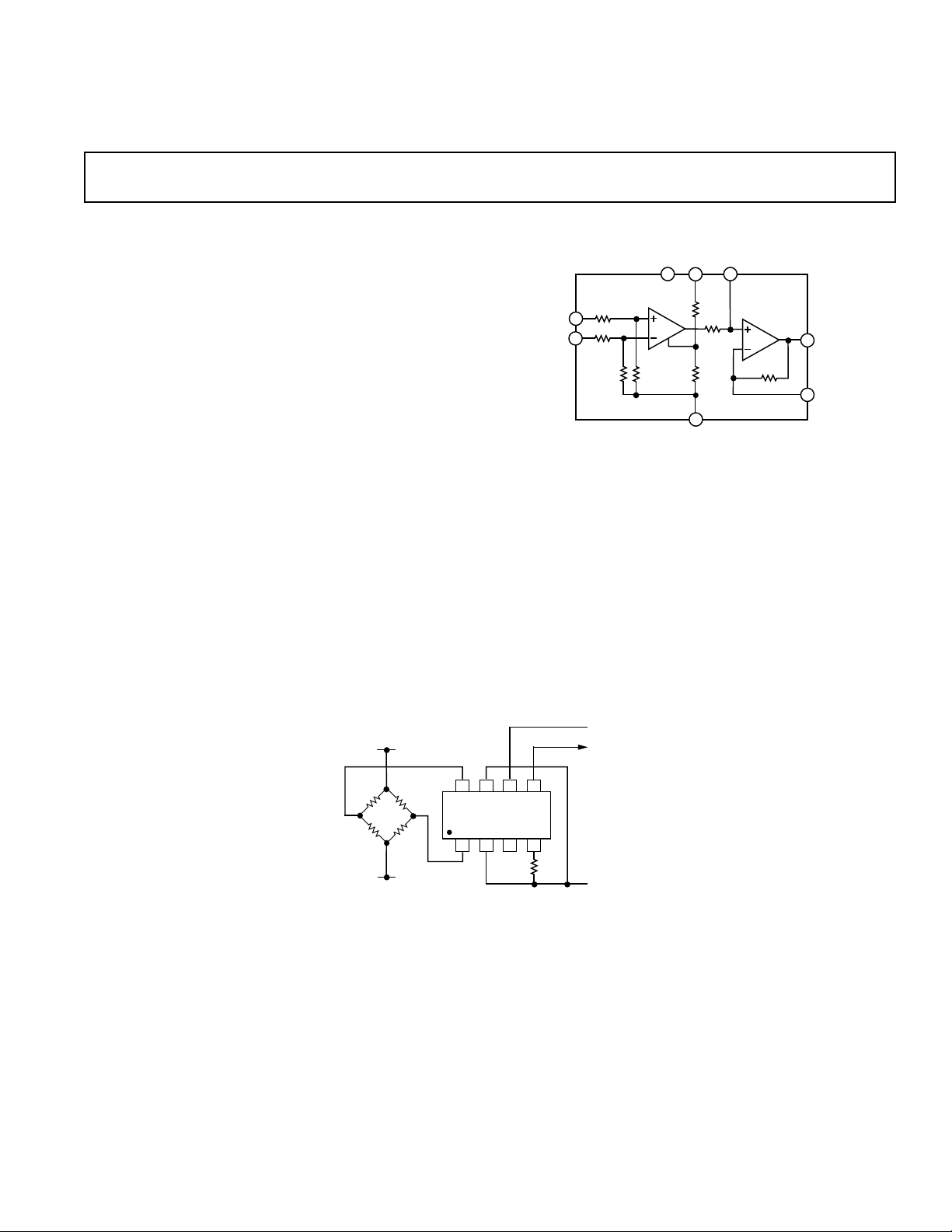
GENERAL DESCRIPTION
The AD22055 accepts a differential signal from a bridge transducer whose common-mode signal can be anywhere between
the power supplies.
V
REF
IN+ OFS +VSOUT
AD22055
IN– GND FILT GAIN
1234
Figure 1. Typical Application Circuit for a Pressure Sensor Interface
The extended temperature range allows for local signal conditioning for oil and hydraulic pressure sensors as well as other
automotive sensors.
The use of an external gain resistor allows the user to compensate transducer gain error and temperature drift.
+5 VOLT
OUTPUT
5678
GAIN = 400
1kΩ
ANALOG
GROUND
REV. 0
Information furnished by Analog Devices is believed to be accurate and
reliable. However, no responsibility is assumed by Analog Devices for its
use, nor for any infringements of patents or other rights of third parties
which may result from its use. No license is granted by implication or
otherwise under any patent or patent rights of Analog Devices.
One Technology Way, P.O. Box 9106, Norwood, MA 02062-9106, U.S.A.
Tel: 617/329-4700 World Wide Web Site: http://www.analog.com
Fax: 617/326-8703 © Analog Devices, Inc., 1997
Page 2

AD22055–SPECIFICATIONS
(@ TA = + 258C, VS = +5 V, VCM = 0, unless otherwise noted)
Parameter Comments Test Conditions Min Typ Max Units
INPUTS (PINS 1 AND 8)
V
CM
CMRR
LF
CMRR
HF
R
INCM
R
MATCH
R
INDIFF
PREAMPLIFIER
G
CL
V
O
R
O
OUTPUT BUFFER
G
CL
V
O
R
O
OVERALL SYSTEM
G
CL
Common-Mode Range 0 5 V
Common-Mode Rejection Ratio f ≤ 10 Hz –80 –90 dB
Common-Mode Rejection Ratio f = 10 kHz –60 –75 dB
Common-Mode Input Resistance Pin 1 or Pin 8 to Pin 2 180 230 kΩ
Matching of Input Resistances ±0.5 %
Differential Input Resistance Pin 1 to Pin 8 180 230 300 kΩ
Closed-Loop Gain
Output Voltage Range (Pin 3) +0.02 +4.75 V
Output Resistance
Closed-Loop Gain
1
2
1
R
≥ 10 kΩ 9.95 10 10.05 V/V
LOAD
77.6 80 82.4 kΩ
40 V/V
Output Voltage Range +0.02 +4.75 V
Output Resistance (Pin 5) V
1
Gain
≥ 0.1 V dc 2.0 Ω
O
V
≥ 0.1 V dc 398 400 402 V/V
O
Gain Drift –40°C to +125°C –60 ppm/°C
Gain Drift –125°C to +150°C –500 ppm/°C
V
OS
Initial Offset Voltage
3
–1 0.05 1 mV
Offset Drift –40°C to +125°C1µV/°C
Offset Drift –125°C to +150°C –10 µV/°C
Input Resistance Pin 7 to Pin 2 2.5 3.0 kΩ
I
OSC
BW
–3 dB
SR Slew Rate 0.2 V/µs
N
SD
Short-Circuit Output Current 7 11 25 mA
–3 dB Bandwidth VO = + 1 V dc 20 30 kHz
Noise Spectral Density
3
f = 100 Hz to 10 kHz 0.2 µV/√Hz
POWER SUPPLY
V
S
I
S
Operating Range TA = T
Quiescent Supply Current
4
MIN
to T
MAX
3 5 36 V
200 500 µA
TEMPERATURE RANGE
T
OP
NOTES
1
A2 gain is trimmed to ±0.5% with a 0.01% 1 kΩ resistor to ground from Pin 4. The overall gain is trimmed to a gain of 400 ±0.5% with the same 1 kΩ resistor. The
gain of A1 (the ratio of overall gain to A2 gain) is used to adjust the overall gain and, therefore, is not trimmed explicitly to 40. Note that the actual gain to a particular application can be modified by the use of an external resistor at Pin 4.
2
The actual output resistance of A1 is only a few ohms, but access to this output, via Pin 3, is always through an 80 k Ω resistor, which is trimmed to ±3%.
3
Referred to the input (Pins 1 and 8).
4
With VDM = 0 V. Differential mode signals are referred to as VDM, while VCM refers to common-mode voltages.
All min and max specifications are guaranteed, although only those marked in boldface are tested on all production units at final test.
Specifications subject to change without notice.
Operating Temperature Range –40 +125 °C
–2–
REV. 0
Page 3

AD22055
Gain = 40 1+
9 kΩ
R
GAIN
V/V
WARNING!
ESD SENSITIVE DEVICE
ABSOLUTE MAXIMUM RATINGS
1
Supply Voltage . . . . . . . . . . . . . . . . . . . . . . . . . +3 V to +36 V
Peak Input Voltage (40 ms) . . . . . . . . . . . . . . . . . . . . . . . .60 V
Reversed Continuous Supply Voltage . . . . . . . . . . . . . . –34 V
Operating Temperature . . . . . . . . . . . . . . . . –40°C to +125°C
Storage Temperature . . . . . . . . . . . . . . . . . . –65°C to +150°C
Output Short Circuit Duration . . . . . . . . . . . . . . . . Indefinite
Lead Temperature (Soldering, 60 sec) . . . . . . . . . . . . . +300°C
1
Stresses above those listed under “Absolute Maximum Ratings” may cause
permanent damage to the device. This is a stress rating only; the functional
operation of the device at these or any other conditions above those indicated in the
operation sections of this specification is not implied. Exposure to absolute
maximum rating conditions for extended periods may affect device reliability.
ORDERING GUIDE
Temperature Package Package
Model Range Description Option*
AD22055N Plastic DIP N-8
AD22055R –40°C to +125°C Plastic SOIC SO-8
*N = Plastic DIP; SO = Small Outline Package.
PIN CONNECTION
IN–
GND
FILT
GAIN
1
AD22055
2
TOP VIEW
(Not to Scale)
3
4
IN+
8
OFS
7
+V
6
S
OUT
5
PRODUCT DESCRIPTION
The AD22055 is a single supply difference amplifier consisting
of a precision balanced attenuator, a very low drift preamplifier
and an output buffer amplifier (A1 and A2, respectively, in the
functional block diagram). It has been designed so that small
differential signals, V
tered in the presence of large common-mode voltages, V
, can be accurately amplified and fil-
DM
CM
,
without the use of any other active components.
The common-mode range resistors in this network are trimmed
to match better than one part in 10,000. The resistive attenuator network is situated at the input to the AD22055 (Pins 1
and 8) allowing the common-mode voltage at Pins 1 and 8 to be
two times greater than that which can be tolerated by the actual
input of A1. As a result, the input common-mode range extends
from ground to the power supply voltage.
Two small filter capacitors (not shown) have been included at
the inputs to A1 to minimize the effects of any spurious RF signals present in the signal.
Internal feedback around A1 sets the closed-loop gain of the
preamplifier to 40 V/V from the input pins, and the output of
A1 is connected to Pin 3 via a 80 kΩ resistor, which is trimmed
to ±3% to facilitate the low-pass filtering of the signal. The output buffer A2 has a gain of 10 V/V (using a precise 1 kΩ resistor
from Pin 4 to ground) setting the precalibrated, overall gain of
the AD22055, to 400 V/V. This gain is easily user-configurable.
Overall gain is programmed using the following equation:
(1)
The dynamic properties of the AD22055 are optimized for
interfacing to transducers, particularly those with a Wheatstone
PIN DESCRIPTION
Bridge configuration. Its rejection of large, high frequency,
common-mode signals makes it superior to that of many alter-
8-Pin SOIC
Pin Function
1 IN–
native approaches. This is due to the very careful design of
the input attenuator and the integration of this highly balanced,
high impedance system with the preamplifier.
2 Ground
3 Filter
4 Gain
5 Out
6+V
S
7 OFS
8 IN+
CAUTION
ESD (electrostatic discharge) sensitive device. Electrostatic charges as high as 4000 V readily
accumulate on the human body and test equipment and can discharge without detection.
Although the AD22055 features proprietary ESD protection circuitry, permanent damage may
occur on devices subjected to high energy electrostatic discharges. Therefore, proper ESD
precautions are recommended to avoid performance degradation or loss of functionality.
REV. 0
–3–
Page 4

AD22055
0.210 (5.33)
MAX
0.160 (4.06)
0.115 (2.93)
0.022 (0.558)
0.014 (0.356)
OUTLINE DIMENSIONS
Dimensions shown in inches and (mm).
8-Lead Plastic DIP
(N-8)
0.430 (10.92)
0.348 (8.84)
8
14
PIN 1
0.100
(2.54)
BSC
5
0.280 (7.11)
0.240 (6.10)
0.060 (1.52)
0.015 (0.38)
0.070 (1.77)
0.045 (1.15)
0.130
(3.30)
MIN
SEATING
PLANE
0.325 (8.25)
0.300 (7.62)
0.015 (0.381)
0.008 (0.204)
8-Lead Plastic SOIC Package
(SO-8)
0.1968 (5.00)
0.1890 (4.80)
C2978–12–1/97
0.195 (4.95)
0.115 (2.93)
0.1574 (4.00)
0.1497 (3.80)
PIN 1
0.0098 (0.25)
0.0040 (0.10)
SEATING
PLANE
8
0.0500
(1.27)
BSC
5
0.2440 (6.20)
41
0.2284 (5.80)
0.0688 (1.75)
0.0532 (1.35)
0.0192 (0.49)
0.0138 (0.35)
0.0098 (0.25)
0.0075 (0.19)
0.0196 (0.50)
0.0099 (0.25)
8°
0°
0.0500 (1.27)
0.0160 (0.41)
x 45°
PRINTED IN U.S.A.
–4–
REV. 0
 Loading...