

Page 1
Class D/1-Bit Audio Power Output Stage
R
R
AD1991
FEATURES
Class D/1-Bit Audio Power Output Stage
5 V Analog and Digital Supply Voltages
Power Stage Power Supply 8 V to 20 V
Output Power @ 0.1% THD + N
Stereo Mode
2 20 W @ 4 @ 14.4 V
2 20 W @ 8 @ 20 V
Mono Mode
1 40 W @ 4 @ 20 V
< 320 m (per Transistor)
R
ON
Efficiency > 85% @ Full Power/8
Clickless Mute Function
Turn-On and Turn-Off Pop Suppression
Short-Circuit Protection
Overtemperature Protection
Data Loss Protection
2-Channel BTL Outputs or
4-Channel Single-Ended Outputs
52-Lead Exposed Pad TQFP Package
Low Cost DMOS Process
APPLICATIONS
PC Audio Systems
Minicomponents
Automotive Amplifiers
Home Theater Systems
Televisions
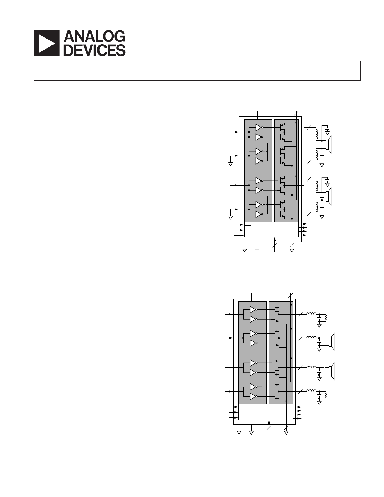
FUNCTIONAL BLOCK DIAGRAMS
2-Channel Mode
INA
LEFT
INPUT
INB
INC
RIGHT
INPUT
IND
CLK
ST/PDN
MUTE
AVDDDV
DD
LEVEL SHIFTER
AND
SWITCH CONTROL
ⴜn
THERMAL PROTECTION
SHORT-CIRCUIT PROTECTION
MUTE CONTROL
AGND DGND
CONTROL
TEST
H-BRIDGE
2 144
A1
A2
B1
B2
C1
C2
D1
D2
PGND
PV
DD
6
4-Channel Mode
OUTA
3
OUTB
3
OUTC
3
OUTD
3
CURRENT OVERLOAD
THERMAL SHUTDOWN
THERMAL WARNING
DATA LOSS
GENERAL DESCRIPTION
The AD1991 is a 2-channel BTL or 4-channel single-ended
class D audio power output stage. The part is configured during
reset to be in either 2-channel mode or 4-channel mode.
To protect the IC as well as the connected speakers, the AD1991
provides turn-on and turn-off pop suppression, short-circuit
protection, and overtemperature shutdown. To control the IC,
a power-down/reset input and a mute pin are available.
The output stage can be operated over a power supply range
from 8 V to 20 V.
In 2-channel mode, Transistors A1, B2, C1, and D2 are turned
on by a Logic 1 on inputs INA and INC, and Transistors A2,
INA
INB
INC
AVDDDV
DD
LEVEL SHIFTER
AND
SWITCH CONTROL
H-BRIDGE
PV
DD
6
A1
OUTA
A2
B1
B2
C1
C2
3
OUTB
3
OUTC
3
LOAD
REQUIRING
DC VOLTAGE
SUPPLY
B1, C2, and D1 are turned on by a Logic 0 on inputs INA and
24 14
TEST
D1
D2
PGND
OUTD
3
CURRENT OVERLOAD
THERMAL SHUTDOWN
THERMAL WARNING
DATA LOSS
LOAD
REQUIRING
DC VOLTAGE
SUPPLY
INC. In 4-channel mode, Transistors A1, B1, C1, and D1 are
turned on by a Logic 1 on the four inputs, and Transistors A2,
IND
B2, C2, and D2 are turned on by a Logic 0 on the four inputs
(see the Functional Block Diagrams).
CLK
ST/PDN
MUTE
REV. 0
Information furnished by Analog Devices is believed to be accurate and
reliable. However, no responsibility is assumed by Analog Devices for its
use, nor for any infringements of patents or other rights of third parties that
may result from its use. No license is granted by implication or otherwise
under any patent or patent rights of Analog Devices. Trademarks and
registered trademarks are the property of their respective companies.
One Technology Way, P.O. Box 9106, Norwood, MA 02062-9106, U.S.A.
Tel: 781/329-4700 www.analog.com
Fax: 781/326-8703 © 2003 Analog Devices, Inc. All rights reserved.
ⴜn
THERMAL PROTECTION
SHORT-CIRCUIT PROTECTION
MUTE CONTROL
AGND DGND
CONTROL
Page 2

AD1991–SPECIFICATIONS
(AVDD = 5 V, DVDD = 5 V, PV
1
Load Impedance = 8 , unless otherwise noted.)
= 20 V, Ambient Temperature = 25C,
DDX
Parameter Min Typ Max Unit Test Conditions
OUTPUT POWER P
(f = 1 kHz SINE WAVE)
O
EFFICIENCY 87 % f = 1 kHz, P
R
ON
2
20 W RL = 4 Ω, PV
20 W R
= 8 Ω, PV
L
DDX
DDX
= 20 W, RL = 8 Ω
O
Per High-Side Transistor 260 320 mΩ @ 1 A
Per Low-Side Transistor 190 235 mΩ @ 1 A
Temperature Coefficient 0.7 mΩ/°C
THERMAL WARNING ACTIVE 135 °CDie temperature
THERMAL SHUTDOWN ACTIVE 150 °CDie temperature
OVERCURRENT SHUTDOWN ACTIVE 3.8 5 6.75 A
POWER SUPPLIES
Supply Voltage AV
Supply Voltage DV
Supply Voltage PV
DD
DD
DDX
4.5 5.0 5.5 V
4.5 5.0 5.5 V
6.5 8 to 20 22.5 V
Power-Down Current
AV
DV
PV
DD
DD
DDX
614µA RST/PDN held low
113µA RST/PDN held low
17 µA RST/PDN held low
Operating Current
AV
DV
PV
DD
DD
DDX
1.8 2.75 mA
4 5.2 mA
40 mA 50:50 384 kHz square wave on
INA and INC
DIGITAL I/O
Input Voltage High 2.0 DV
DD
V
Input Voltage Low 1.2 V
Output Voltage High DV
– 0.8 V @ 2 mA
DD
Output Voltage Low 0.4 V @ 2 mA
Leakage Current on Digital Inputs 10 µA
NOTES
1
Performance of both channels is identical.
2
Measurement requires PWM modulator.
Specifications subject to change without notice.
= 14 V
= 20 V
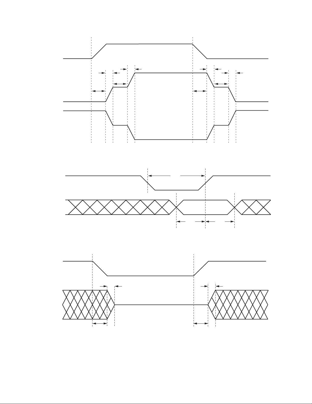
DIGITAL TIMING CHARACTERISTICS
(Guaranteed over –40C to +85C, AVDD = DVDD = 5 V 10%, PV
Edge Speed = Slowest, Nonoverlap Time = Shortest.)
= 20 V 10%,
DDX
Symbol Parameter Min Typ Max Unit
t
PDL
t
PST
t
NOL
t
PDRP
t
MSU
t
MH
t
MPDL
Specifications subject to change without notice.
Input transition to output initial response 30 ns
Power transistor switching time 3.5 ns
Nonoverlap time 25 to 40 ns
RST/PDN minimum low pulsewidth 20 ns
Mode pin setup time before RST/PDN going high 5 ns
Mode pin hold time after RST/PDN going high 5 ns
MUTE asserted to output initial response 3 s
REV. 0–2–
Page 3
AD1991
R
M
INA
OUTA
OUTB
ST/PDN
t
PDL
t
PST
t
PST
t
NOL
t
t
PST
t
PDL
PST
t
NOL
Figure 1. Output Timing
t
PDRP
MODEx
t
MSU
Figure 2.
UTE
t
PST
OUTx
t
MPDL
RESET
Figure 3.
and Mode Timing
MUTE
Timing
t
MPDL
t
MH
t
PST
REV. 0
–3–
Page 4

AD1991
ABSOLUTE MAXIMUM RATINGS
(TA = 25°C, unless otherwise noted.)
1
AVDD, DVDD to AGND, DGND . . . . . . . . . . –0.3 V to +6.5 V
to PGNDx2 . . . . . . . . . . . . . . . . . . . –0.3 V to +30.0 V
PV
DDX
AGND to DGND to PGNDx . . . . . . . . . . . . –0.3 V to +0.3 V
to DVDD . . . . . . . . . . . . . . . . . . . . . . . –0.5 V to +0.5 V
AV
DD
Operating Temperature Range (Ambient)
Industrial . . . . . . . . . . . . . . . . . . . . . . . . . –40°C to +85°C
Storage Temperature Range . . . . . . . . . . . . –65°C to +150°C
Maximum Junction Temperature . . . . . . . . . . . . . . . . . 150°C
Thermal Resistance3 . . . . . . . . . . . . . . . . . . . . . . . 1°C/W
θ
JC
Lead Temperature
Soldering (10 sec) . . . . . . . . . . . . . . . . . . . . . . . . . . . 260°C
Vapor Phase (60 sec) . . . . . . . . . . . . . . . . . . . . . . . . . 215°C
Infrared (15 sec) . . . . . . . . . . . . . . . . . . . . . . . . . . . . 220°C
ORDERING GUIDE
Temperature Package Package
Model Range Description Option
AD1991ASV –40°C to +85°CThin Quad Flat Pack [TQFP] SV-52
AD1991ASVRL –40°C to +85°CThin Quad Flat Pack [TQFP] SV-52
EVAL-AD1991EB Evaluation Board
NOTES
1
Stresses above those listed under Absolute Maximum Ratings may cause permanent damage to the device. This is a stress rating only; functional operation of the
device at these or any other conditions above those listed in the operational
sections of this specification is not implied. Exposure to absolute maximum rating
conditions for extended periods may affect device reliability. Only one absolute
maximum rating may be applied at any one time.
2
Including any induced voltage due to inductive load.
3
With respect to the temperature of the exposed pad.
CAUTION
ESD (electrostatic discharge) sensitive device. Electrostatic charges as high as 4000 V readily
accumulate on the human body and test equipment and can discharge without detection. Although the
AD1991 features proprietary ESD protection circuitry, permanent damage may occur on devices
subjected to high energy electrostatic discharges. Therefore, proper ESD precautions are recommended
to avoid performance degradation or loss of functionality.
REV. 0–4–
Page 5

PIN CONFIGURATION
AD1991
AGND
AGND
MODE1
AD1991
TOP VIEW
(Not to Scale)
INB
INA
ERR0
AV
DV
DD
DD
AGND
MODE0
MUTE
DGND
AGND
PGND2
IND
INC
PGND2
PGND2
CLK
RST/PDN
39
38
37
36
35
34
33
32
31
30
29
28
27
PGND2
OUTC
OUTC
OUTC
PV
DD2
PV
DD2
PV
DD2
OUTD
OUTD
OUTD
PGND2
PGND2
PGND2
PGND1
OUTA
OUTA
OUTA
PV
DD1
PV
DD1
PV
DD1
OUTB
OUTB
OUTB
PGND1
PGND1
PGND1
PGND1
PGND1
PGND1
52 51 50 49 48 43 42 41 4047 4 6 45 44
1
PIN 1
2
IDENTIFIER
3
4
5
6
7
8
9
10
11
12
13
14 15 16 17 18 19 20 21 22 23 24 25 26
ERR3
ERR2
ERR1
PIN FUNCTION DESCRIPTIONS
Pin No. Mnemonic In/Out Description
1 PGND1 Negative power supply for high power Transistors A2 and B2.
2, 3, 4 OUTA O Output of transistor pair A1 and A2.
5, 6, 7 PV
DD1
Positive power supply for high power Transistors A1 and B1.
8, 9, 10 OUTB O Output of transistor pair B1 and B2.
11, 12, 13 PGND1 Negative power supply for high power Transistors A2 and B2.
14 ERR3 I/O Edge speed setting MSB during RESET/active low thermal shutdown error output during
normal operation.
15 ERR2 I/O Edge speed setting Bit 1 during RESET/active low thermal warning error output during
normal operation.
16 ERR1 I/O Nonoverlap time setting MSB during RESET/active thermal low shutdown error output
during normal operation.
17 ERR0 I/O Nonoverlap time setting Bit 1 during RESET/active low data-loss error output or low-side
transistor disable input during normal operation.
18 INA I Control pin for Transistors A1 and A2 always; also control pin for B1 and B2 in 2-channel mode.
19 INB I Edge speed setting LSB during RESET/during normal operation, control pin for Transistors
B1 and B2 in 4-channel mode; no function in 2-channel mode.
20 DV
DD
Positive power supply for low power digital circuitry.
21 DGND Negative power supply for low power digital circuitry.
22 MUTE I Active low clickless mute input.
23 INC I Control pin for Transistors C1 and C2 always; also control pin for D1 and D2 in 2-channel mode.
24 IND I Nonoverlap time setting LSB during RESET/during normal operation, control pin for Transis-
tors D1 and D2 in 4-channel mode; no function in 2-channel mode.
25 RST/PDN I Active low RESET/power-down input.
26 CLK I External clock input in external clock mode.
27, 28, 29 PGND2 Negative power supply for high power Transistors C2 and D2.
30, 31, 32 OUTD O Output of transistor pair D1 and D2.
33, 34, 35 PV
DD2
Positive power supply for high power Transistors C1 and D1.
36, 37, 38 OUTC O Output of transistor pair C1 and C2.
39, 40, 41, 42 PGND2 Negative power supply for high power Transistors C2 and D2.
43, 45, 48, 49 AGND Negative power supply for low power analog circuitry.
44 MODE0 Clock source select (referenced to AGND); normally connected to AGND.
46 AV
DD
Positive power supply for low power analog circuitry.
47 MODE1 I Channel mode select (referenced to AGND).
50, 51, 52 PGND1 Negative power supply for high power Transistors A2 and B2.
REV. 0
–5–
Page 6

AD1991
FUNCTIONAL DESCRIPTION
Device Architecture
The AD1991 is an 8-transistor, audio, power output stage. The
AD1991 is arranged internally as four transistor pairs that can
be used as two H-bridge outputs (2-channel mode) or as four
single-ended outputs (4-channel mode), using either two or four
TTL compatible inputs to control the transistors. A dead time
is automatically provided between the switching of the highside transistor and low-side transistor when the control inputs
change level, to ensure that both the high-side transistor and
low-side transistor are never on at the same time.
Clock Source and Channel Mode Selection
When the AD1991 is brought out of reset, the logic levels on
MODE0 and MODE1 are latched internally. MODE0 determines
the internal state machine clock source. MODE1 determines the
channel mode and the function of ERR0 (see Tables I and II.)
When the internal clock is used, the CLK pin should not be
connected.
Table I. Clock Source Selection
MODE0 CLK Source
0 Internal
1External
Table II. Channel Mode Selection
MODE1 Channel Mode ERR0 Function
0 2-Channel Mode Data Loss Detection Output
1 4-Channel Mode Low-Side Disable Input
2-Channel Mode
Two loads are connected differentially—across OUTA and OUTB
and across OUTC and OUTD. Inputs INB and IND are unused
and should be tied to an appropriate dc voltage (see the Edge
Speed and Nonoverlap Settings section). In this mode, ERR0 is
an error output used to indicate data loss, which occurs when
there are no transitions on INA or INC for more than 50 ms.
This signal condition is hazardous in 2-channel mode because it
can cause a potentially large and harmful dc voltage across the
differential loads. Table III shows the input/output relationship.
Table III. Input/Output Relationship in 2-Channel Mode
Input Controlled Output
INA OUTA, OUTB
INC OUTC, OUTD
4-Channel Mode
The 4-channel mode has two types of configuration: audio and
power supply. Neither of these configurations require data loss
detection. In the audio configuration, each single-ended load is
connected to the output through a blocking capacitor, which
prevents dc from reaching the load, thereby negating the need
for data loss detection. While in the power supply configuration,
it is desired to maintain a dc voltage on the load, also negating
the need for data loss detection. When used in the power supply
configuration, the four low-side transistors can also be disabled
and left permanently open if desired. This allows the loads to be
driven by switching only the high-side transistor on and off.
ERR0 is an input in 4-channel mode and is used to select
whether the four low-side transistors are enabled or disabled,
with 0 selecting disabled and 1 selecting enabled. Table IV
summarizes the function of ERR0 in this mode. Table V shows
the input/output relationship.
Table IV. ERR0 Function in 4-Channel Mode
ERR0 Low-Side Transistor Status
0 Disabled
1 Enabled
Table V. Input/Output Relationship in 4-Channel Mode
Input Controlled Output
INA OUTA
INB OUTB
INC OUTC
IND OUTD
1-Channel Mode
One load is connected differentially—across OUTA and OUTC,
and OUTB and OUTD. This mono operation is established
by configuring the part for 2-channel mode and externally
connecting INA to INC, OUTA to OUTC, and OUTB to
OUTD (see Figure 4).
Thermal Protection
The AD1991 features thermal protection. When the die temperature exceeds approximately 135°C, the thermal warning error
output (ERR2) is asserted. If the die temperature exceeds
approximately 150°C, the thermal shutdown error output (ERR3)
is asserted. If this occurs, the part shuts down to prevent damage
to the part. When the die temperature drops below approximately
120°C, both error outputs de-assert and the part returns to normal operation.
Overcurrent Protection
The AD1991 features overcurrent or short-circuit protection. If
the current through any power transistors exceeds 5 A, the part
is muted and the overcurrent error output (ERR1) is asserted.
This is a latched error and does not clear automatically. To clear
the error condition and restore normal operation, the part must
be reset or MUTE must be asserted and de-asserted.
REV. 0–6–
Page 7

INPUT
R
ST/PDN
MUTE
INA
INB
INC
IND
CLK
DV
DD
DD
LEVEL SHIFTER
AND
SWITCH CONTROL
n
THERMAL PROTECTION
SHORT-CIRCUIT PROTECTION
MUTE CONTROL
AGND DGND
CONTROL
TEST
A1
A2
B1
B2
H-BRIDGE
C1
C2
D1
D2
24 14
PGND
PV
DD
6
OUTA
3
OUTB
3
OUTC
3
OUTD
3
CURRENT OVERLOAD
THERMAL SHUTDOWN
THERMAL WARNING
DATA LOSS
AV
Figure 4. Functional Block Diagram (1-Channel Mode)
EDGE SPEED AND NONOVERLAP SETTINGS
The AD1991 allows the user to select from one of eight different
edge speeds and from one of eight different nonoverlap times.
This allows the user to make a trade-off between distortion,
efficiency, overshooting at the outputs, and EMI. The following
sections describe the method used to program the settings.
Edge Speed
The edge speed is set by using the three pins, ERR3, ERR2, and
INB, when RST/PDN is low. The levels on the three pins are
latched by the rising edge of RST/PDN. The latched value determines the edge speed thereafter, until RST/PDN is brought low.
Table VI shows the appropriate logic levels for the corresponding
edge speeds. Note that INB is internally inverted, resulting in
the nonmonotonic sequence in Table VI.
AD1991
Table VI. Edge Speed Settings
ERR3 ERR2 INB Edge Speed
0011 (Slowest Edge Speed)
0002
0113
0104
1015
1006
1117
1108 (Fastest Edge Speed)
Nonoverlap Time
The nonoverlap time is set by using the three pins, ERR1, ERR0,
and IND, when RST/PDN is low. The levels on the three pins
are latched by the rising edge of RST/PDN. The latched value
determines the nonoverlap time thereafter, until RST/PDN is
brought low. Table VII shows the appropriate logic levels for
the corresponding nonoverlap times. Note that IND is internally
inverted, resulting in the nonmonotonic sequence in Table VII.
Note that ERR3, ERR2, ERR1, and ERR0 are driven outputs
under normal operation and, therefore, should never be tied to a
dc voltage. The part contains internal 300 kΩ pull-up resistors
to pull these pins high during reset. If it is desired to set them
low to achieve a particular edge speed or nonoverlap time, this
should be done by pulling them low through resistors between
10 kΩ and 50 kΩ.
Table VII. Nonoverlap Time Settings
ERR1 ERR0 IND Nonoverlap Time
00 11 (Shortest Nonoverlap Time)
00 02
01 13
01 04
10 15
10 06
11 17
11 08 (Longest Nonoverlap Time)
REV. 0
–7–
Page 8

AD1991
APPLICATION CONSIDERATIONS
Good board layout and decoupling are vital for correct operation
of the AD1991. Due to the fact that the part switches high currents,
there is the potential for large PV
bounce each time a transis-
DD
tor transitions. This can cause unpredictable operation of the part.
To avoid this potential problem, close chip decoupling is essential. It is also recommended that the decoupling capacitors be
placed on the same side of the board as the AD1991 and connected
directly to the PV
and PGND pins. By placing the decoupling
DD
capacitors on the other side of the board and decoupling through
vias, the effectiveness of the decoupling is reduced. This is
because vias have inductive properties and, therefore, prevent
very fast discharge of the decoupling capacitors. Best operation
is achieved with at least one decoupling capacitor on each side of
the AD1991 or optionally two capacitors per side can be used to
further reduce the series resistance of the capacitor. If these
decoupling recommendations cannot be followed and decoupling
through vias is the only option, the vias should be made as large
as possible to increase surface area, thereby reducing inductance
and resistance.
Figures 5 and 6 show two possible layouts to provide close chip
decoupling. In both cases, the PV
to PGND decoupling is as
DD
close as possible to the pins of the AD1991. One solution uses
surface-mount capacitors that offer low inductance; however, each
output (OUTA, OUTB, OUTC, and OUTD) must be brought
through vias to another layer of the board to be brought to the
LC filter. The other solution uses through-hole capacitors that
have higher inductance but allow the outputs to connect directly
to the LC filter. In this solution, the inductor for OUTA and
OUTC would span the PV
decoupling capacitors from PV
trace. These diagrams show four
DD
to PGND; however, this may
DD
not be necessary if capacitors with low series resistance are
used. Another close chip capacitor is used for AV
to AGND
DD
decoupling, with the actual power connections to the capacitors
being done through vias. This is quite acceptable since AV
DD
is
a low current stable supply. Finally, a close chip capacitor is used
to decouple DV
to DGND. This is quite important since DV
DD
DD
is a digital supply whose current will change dynamically and,
therefore, requires good decoupling. For both PV
and DVDD,
DD
additional reservoir capacitors should be used to augment the
close chip decoupling, especially for PV
, which usually has very
DD
large transients.
junction (die) and the case (package) for each watt of power
dissipated in the die. The AD1991 is specified with a
of
JC
1°C/W, which means that for each watt of power dissipated in
the part, the junction (or die) temperature will be 1ºC higher
than the case (or package) temperature.
The value of
, the difference between the case and ambient
CA
temperatures, is entirely dependent on the size of heat sink
attached to the case, the material used, the method of attachment, and the airflow over the heat sink. The value of
CA
is
specified as 26°C/W for no heat sink and no airflow over the device.
Finally,
is the sum of the JC and CA values, and will be
JA
between 1°C/W and 27°C/W depending on the heat sink used.
This is the temperature difference between the junction (die) and
ambient temperature around the case (package) for each watt
dissipated in the part.
The AD1991 is specified to have a thermal shutdown of typically
150°C die temperature. Good design procedures allow for a
margin, so the system should be designed such that the AD1991
die never goes above 140°C. Knowing the maximum desirable
die temperature, the efficiency of the AD1991, the maximum
ambient temperature, and the maximum power that will be
delivered to the load, the necessary
can be calculated. For an
CA
8 Ω load, the AD1991 has a typical efficiency of 87%, which
can be reduced slightly to be conservative. For this example,
assume an 85% efficiency. If the power delivered to the loads is
to be 2 ⫻ 20 W rms continuous power, the power dissipated in
the AD1991 can be calculated as follows:
Power Supplied to Loads = 40 W rms
⫻
Total Power Supplied to the AD1991 = (40/85
100) = 47 W rms
Power Dissipated in the AD1991 = 7 W rms
If the ambient temperature can reach 85°C maximum, the allowable
difference between the die temperature and ambient temperature
is (140 – 85) = 55°C. This gives a JA requirement of (55/7) =
7.9°C/W. This requires a heat sink that gives a
of 6.9°C/W.
CA
The size and type of heat sink required can now be calculated.
If adequate heat sinking is not applied to the AD1991, the system
will suffer from the AD1991 going into thermal shutdown. It is
advisable to also use the thermal warning output on the AD1991
to attenuate the power being delivered to help prevent thermal
shutdown.
THERMAL CONSIDERATIONS
Careful consideration must be given to heat sinking the AD1991,
particularly in applications where the ambient temperature can
be much higher than normal room temperature. The three
thermal resistances of
, CA, and
JC
should be known in
JA
order to correctly heat sink the part. These values specify the
temperature difference between two points, per unit power
dissipation.
specifies the temperature difference between the
JC
POWER-UP CONSIDERATIONS
Careful power-up is necessary when using the AD1991 to
ensure correct operation and to avoid possible latch-up issues.
The AD1991 should be held in RESET with MUTEB asserted
until all three power supplies have stabilized. Once the supplies
have stabilized, the part can be brought out of RESET, and
following this, MUTEB can be negated.
REV. 0–8–
Page 9

CAPCAP
PVDD PLANE
CAP
1
2
3
4
5
6
7
8
9
10
11
12
13
14 15 16 17 18 19 20 21 22 23 24 25 26
AGND PLANE
PGND
PLANE
AD1991
40414243444546474849505152
39
38
37
36
35
34
33
32
31
30
29
28
27
CAP CAP
CAP
Figure 5. Layout Using Surface-Mount Capacitors (4 × 10 nF or 2 × 22 nF Recommended)
PVDD PLANE
CAP
40414243444546474849505152
39
38
37
36
35
34
33
32
31
CAP CAP
30
29
28
27
CAPCAP
1
2
3
4
5
6
7
8
9
10
11
12
13
161514 26252423222120191817
AGND PLANE
PGND
PLANE
REV. 0
CAP
Figure 6. Layout Using Through-Hole Capacitors (4 × 10 nF or 2 × 22 nF Recommended)
–9–
Page 10

AD1991
DD
AD1991
PV
DD
PV
DD
PGND
ANALOG INPUT_L
GND
ANALOG INPUT_R
AV
DV
DD
DD
AV
DDDVDD
AGND DGND FEEDBACK
AGND
FEEDBACK
MODULATOR
DGND
AVDDDV
PWM_L
GND
PWM_R
AGND DGND PGND
Figure 7. Simplified System Schematic for Analog-In, Analog-Out System
REV. 0–10–
Page 11

OUTLINE DIMENSIONS
52-Lead Thin Quad Flat Package, Exposed Pad [TQFP/EP]
(SV-52)
Dimensions shown in millimeters
12.00
BSC SQ
1
TOP VIEW
(PINS DOWN)
4052
39
10.00
BSC SQ
40 52
39
BOTTOM VIEW
(PINS UP)
EXPOSED
PAD
1
6.50
SQ
AD1991
1.20
MAX
13
14
VIEW A
0.20
0.09
COMPLIANT TO JEDEC STANDARDS MS-026ACC
WITH THE EXCEPTION THAT THE EXPOSED DIE PAD SHALL BE
COPLANAR WITH BOTTOM OF PACKAGE WITHIN 0.05 MILLIMETERS.
27
26
SEATING
1.05
1.00
0.95
PLANE
27
26
0.15
0.05
0.65
BSC
VIEW A
7
3.5
0
0.75
0.60
0.45
0.38
0.32
0.22
13
14
REV. 0
–11–
Page 12

C03587–0–5/03(0)
–12–
 Loading...