

Page 1
Class-D Audio Power Amplifier
Preliminary Technical Data
FEATURES
Integrated Stereo Modulator & Power Stage
0.005% THD+N
101.5dB Dynamic Range
PSRR > 65 dB
< 0.3 Ω (per transistor)
R
DS-ON
Efficiency > 80% @ 5W/6 Ω
EMI Optimized Modulator
On-Off-Mute Pop Noise Suppression
Short Circuit Protection
Over-Temperature Protection
Low Cost DMOS Process
APPLICATIONS
Flat Panel Televisions
Automotive Amplifiers
PC Audio Systems
Mini Components
AD1990/AD1992/AD1994/AD1996
GENERAL DESCRIPTION
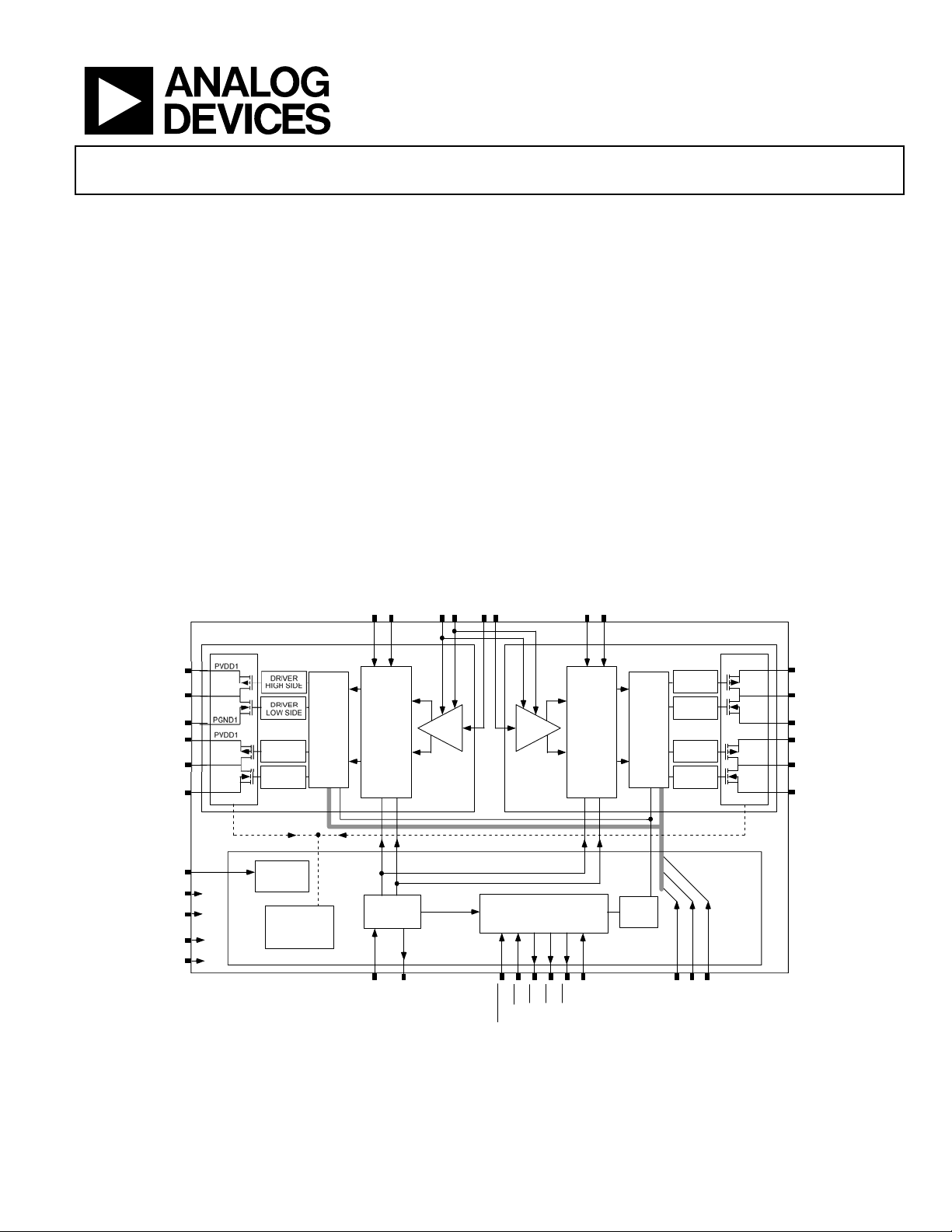
The AD199x is a two channel Bridge Tied Load (BTL)
switching audio power amplifier with integrated
The modulator accepts a 1Vrms input signal (maximum power)
and generates a switching waveform to drive speakers directly.
One of the two modulators can control both output stages
providing twice the current for single-channel applications. A
digital, microcontroller-compatible interface provides control of
reset, mute and PGA gain as well as output signals for thermal
and over-current error conditions. The output stage can operate
from supply voltages ranging from 8V to 20V. The analog
modulator and digital logic operate from a 5V supply.
AD1990: 5Wx2 (10Wx1)
AD1992: 10Wx2 (20Wx1)
AD1994: 25Wx2 (50Wx1)
AD1996: 40Wx2 (80Wx1)
0
+
-
L
L
F
F
N
N
62
63
1
L
A
G
P
3132
N
I
A
60 53
R
N
I
A
A
G
P
+
R
F
N
50 51
R
F
N
∑∆ modulator.
PVDD
OUTL+
PGND1
PVDD1
11,12,13
OUTL-
14,15,16
PGND1
REF_FILT
AVDD
AGND
DVDD
DGND
7,8
4,5,6
1,2,3
9,10
PGND1
55
57
56
24,25
23,26
LEFT CHANNEL
CONTROL
DRIVER
HIGH SIDE
DRIVER
LOW SIDE
VOLTAGE
REFERENCE
TEMPERATURE
SENSE &
OVER-CURRENT
PROTECTION
LEVEL
SHIFT
+
DEAD
TIME
Σ∆
MODULATOR
Ø1 Ø2
OSCILLATOR
27 28 22 21 20
CLKI
PGA
CLKO
Figure 1. Block Diagram
Rev. PrA – 1/20/05
Information furnished by Analog Devices is believed to be accurate and reliable.
However, no responsibility is assumed by Analog Devices for its use, nor for any
infringements of patents or other rights of third parties that may result from its use.
Specifications subject to change without notice. No license is granted by implication
or otherwise under any patent or patent rights of Anal og Devices. Trademarks and
registered trademarks are the property of their respective companies.
RIGHT CHANNEL
DRIVER
HIGH SIDE
DRIVER
LEVEL
LOW SIDE
SHIFT
+
DEAD
TIME
CONTROL
MUTE/
POP
CONTROL
DRIVER
HIGH SIDE
DRIVER
LOW SIDE
0
L
R
T
C
D
www.analog.com
18
17
1
R
R
E
Σ∆
MODULATOR
Ø1 Ø2
49
2
O
R
N
R
O
E
M
PGA
MODE CONTROL LOGIC
19
29
30
0
E
N
R
T
D
R
U
W
E
M
P
/
T
S
R
One Technology Way, P.O. Box 9106, Norwood, MA 02062-9106, U.S.A.
Tel: 781.329.4700
Fax: 781.326.8703 © 2005 Analog Devices, Inc. All rights reserved.
PVDD2
PGND2
PVDD2
PGND2
2
1
L
L
R
R
T
T
C
C
D
D
41,42
PVDD2
43,44,45
OUTR+
46,47,48
PGND2
39,40
PVDD2
36,37,38
OUTR-
33,34,35
PGND2
Page 2

AD199x Preliminary Technical Data
TABLE OF CONTENTS
General Description ........................................................................ 1
AD199x—Specifications.................................................................. 3
test conditions unless otherwise noted...................................... 3
Absolute Maximum Ratings............................................................ 6
Pin Configurations And Functional Descriptions....................... 7
Typical Performance Characteristics ............................................. 8
Functional Description.................................................................. 10
Device Architecture ................................................................... 10
Amplifier Gain............................................................................ 10
System Design............................................................................. 11
Outline Dimensions....................................................................... 14
ESD Caution................................................................................ 14
Rev. PrA – 1/20/05 | Page 2 of 16
Page 3

Preliminary Technical Data AD199x
AD199X—SPECIFICATIONS
TEST CONDITIONS UNLESS OTHERWISE NOTED
Supply Voltages
AV
5 V
DD
DV
5 V
DD
PV
12 V
DDX
Ambient Temperature 25 °C
Load Impedance 6 Ω
Clock Frequency 11.2896 MHz
Measurement Bandwidth 20 Hz to 20 KHz
Table 1. Performance of both channels is identical
Parameter Min Typ Max Units Test Conditions/Comments
OUTPUT POWER (PO)
AD1990
AD1992
AD1994
AD1996
Efficiency 84 %
RON
per High Side Transistor
per Low Side Transistor
Maximum Current Through OUTx 4 A
Thermal Warning Active 135 °C Die temperature
Thermal Shutdown Active 150 °C Die temperature
Overcurrent Shutdown Active 4 A
Nominal Input Level 1.0 V
Modulation Factor 90 %
PERFORMANCE SPECIFICATIONS
Total Harmonic Distortion (THD+N) 0.005 % PGA = 0 dB, PO = 5 W
0.007 % PGA = 6 dB, PO = 5 W
0.01 % PGA = 12 dB, PO = 5 W
0.02 % PGA = 18 dB, PO = 5 W
Signal/Noise Ratio (SNR) 102 dB
Dynamic Range (DNR) 102 dB -60 dB Input
Crosstalk
Power supply rejection (PSRR)
60
45
DC SPECIFICATIONS
Input Impedance 20
Output DC Offset Voltage ±10 mV
4
5
8
10
16
25
25
40
-100
0.3
0.2
R
= 6Ω, PVDD = 20 V, 1 kHz (FTC)
W
W
W
W
W
W
W
W
Ω
Ω
PGA gain = 0 dB
RMS
dB
dB
dB
kΩ
L
@ <0.01% THD+N
@ 10% THD+N (FTC)
@ <0.01% THD+N
@ 10% THD+N (FTC)
@ <0.01% THD+N
@ 10% THD+N (FTC)
@ <0.01% THD+N
@ 10% THD+N (FTC)
f
=1 kHz, PO = 5 W, RL = 6Ω
IN
@ 1 A
@ 1 A
Measured channel input = 0 V
other channel = 1 kHz at 5W
20 Hz - 1 kHz
20 Hz – 20 kHz
AINL and AINR analog inputs
RMS
,
Rev. PrA – 1/20/05 | Page 3 of 16
Page 4

AD199x Preliminary Technical Data
Parameter Min Typ Max Units Test Conditions/Comments
POWER SUPPLIES
Supply Voltage AVDD 4.5 5 5.5 V
Supply Voltage DVDD 4.5 5 5.5 V
Supply Voltage PV
Powerdown Current
AVDD 0.1 0.5 µA
DVDD 0.1 0.5 µA
PV
19 25 µA
DDX
Mute Current
AVDD 19 mA
DVDD 2.7 mA
PVDD 1.5 mA
Quiesent Current Inputs Grounded, Non-Overlap Time = TBD
AVDD 20 mA
DVDD 5.2 mA
PV
3.2 mA
DDX
Operating Current VIN = 1V
AVDD 22 mA
DVDD 5.8 mA
PVDD 4 A per FET
DIGITAL I/O
Input Voltage High 2.0 DVDD V
Input Voltage Low 0.8 V
Output Voltage High DVDD-0.8 V @ 2 mA
Output Voltage Low 0.4 V @ 2 mA
Leakage Current on Digital Inputs 10 µA
6.5 8-20 22.5 V
DDX
RST/PDN
MUTE
held low
held low
, PO = 5 W
RMS
Rev. PrA – 1/20/05 | Page 4 of 16
Page 5
Preliminary Technical Data AD199x
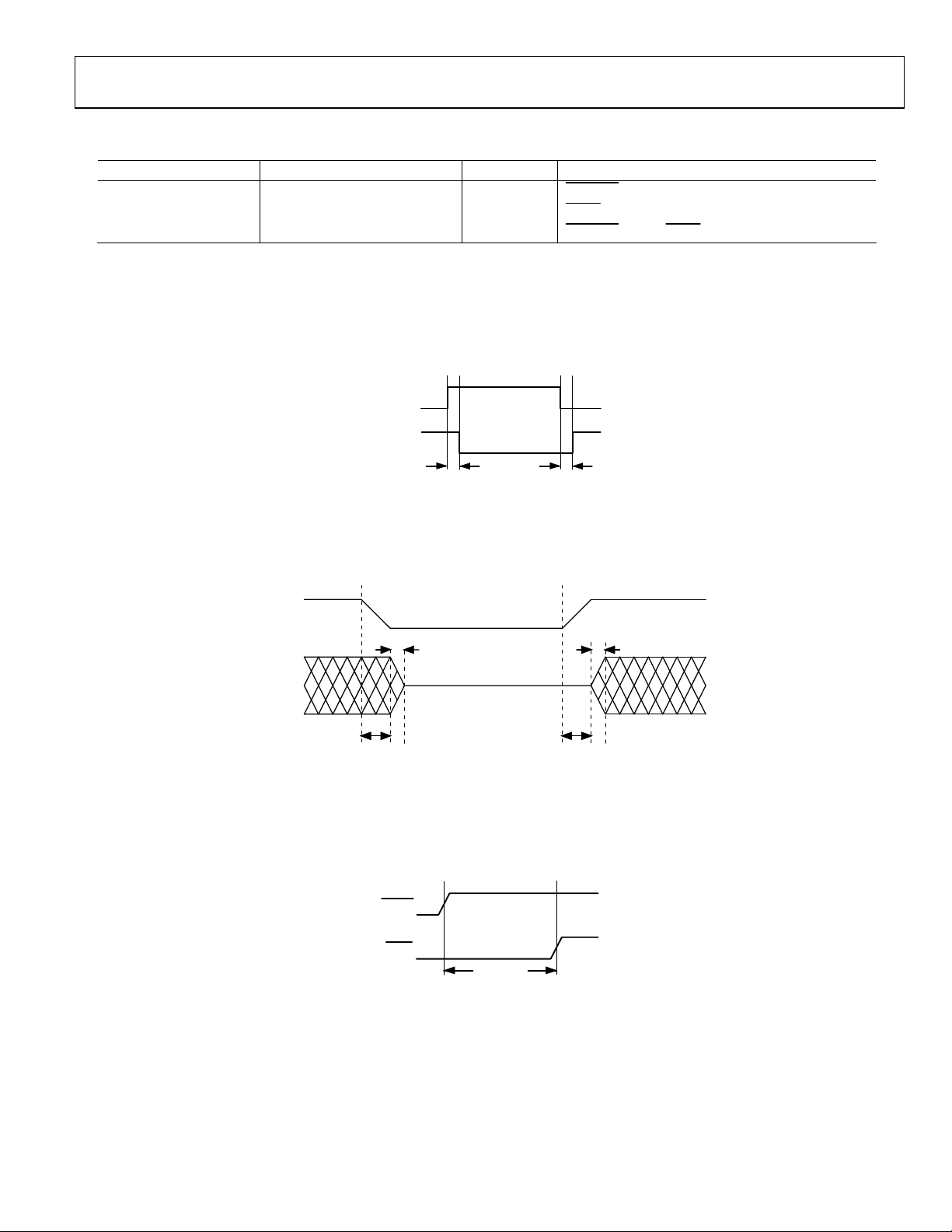
Table 2 DIGITAL TIMING (Guaranteed over -40°C to +85°C, AV
= Shortest, See Table 6: Non-Overlap Time Settings)
t
NOL
Parameter Min Typ Max Units Comments
t
500 ns
PDRP
t
MPDL
t
1 sec
MUTEDLY
5 µs
OUTL+/
OUTR+
OUTL-/
OUTR-
= DVDD = 5.0V ± 10%, PV
DD
RST/PDN
MUTE
asserted to output initial response
RST/PDN
=12V ± 10%, Non Overlap Time
DDX
minimum low pulsewidth
high to
MUTE
high delay
MUTE
OUTX
t
MPDL
t
PST
RESET
t
NOL
Figure 2. Output Timing
Figure 3. Mute Ti ming
t
NOL
t
MPDL
t
PST
MUTE
t
MUTEDLY
Figure 4. Reset to Mute Delay
Rev. PrA – 1/20/05 | Page 5 of 16
Page 6

AD199x Preliminary Technical Data
ABSOLUTE MAXIMUM RATINGS
1
Table 3. AD199x Absolute Maximum Ratings
Parameter Rating
AVDD, DVDD to AGND, DGND -0.3 V to +6.5 V
PV
to PGND -0.3 V to +30.0 V2
DDX
AGND to DGND to PGND -0.3 V to +0.3 V
AVDD, to DVDD -0.5 V to +0.5 V
Audio Inputs AGND to AVDD
Operating Temperature Range –40°C to +85°C
Storage Temperature Range –65°C to +150°C
Maximum Junction Temperature 150°C
θJC Thermal Impedance (LFCSP)
θJC Thermal Impedance (PSOP)
3°C/W
1°C/W
Lead Temperature
Soldering (10 sec) 260°C
Vapor Phase (60 sec) 215°C
Infrared (15 sec) 220°C
1
Stresses above those listed under Absolute Maximum Ratings
may cause permanent damage to the device. This is a stress
rating only and functional operation of the device at these or
any other condition s above those indicated in the operational
section of this specification is not implied. Exposure to absolute
maximum rating conditions for extended periods may affect
device reliability. Only one absolute maximum rating may be
applied at any one time.
2
Including any induced voltage due to inductive load
PGND1
PGND1
PGND1
OUTL+
OUTL+
OUTL+
PV
DD1
PV
DD1
PV
DD1
PV
DD1
OUTL-
OUTL-
OUTL-
PGND1
PGND1
PGND1
D
-
+
N
L
G
F
A
N
•
1
PIN 1
IDEN T IFIER
2
3
4
5
6
7
8
9
10
11
12
13
14
15
16
17 18 19 20 21 22 23 24 25 26
1
2
R
R
R
R
E
E
L
L
N
C
F
N
N
C
I
C
A
N
N
AD1990/92/94
TOP VIE W
(Not to Scale)
2
0
1
0
L
R
R
R
T
E
C
D
D
L
L
N
R
R
G
T
T
D
C
C
D
D
Figure 5. 64 Lead LFCSP Package
T
L
I
F
D
D
_
N
D
G
V
A
A
D
D
D
D
V
V
D
D
R
F
N
C
E
R
27 28 29 30 31 32
D
N
G
D
C
I
N
N
A
52
I
E
O
K
T
K
L
U
L
C
C
M
R
F
N
1990-0002
N
D
P
/
T
S
R
O
+
N
R
O
F
M
N
49505164 63 62 61 60 59 58 57 56 55 54 53
PGND2
48
PGND2
47
46
PGND2
OUTR+
45
OUTR+
44
OUTR+
43
PV
42
DD2
PV
41
DD2
PV
40
DD2
PV
39
DD2
OUTR-
38
OUTR-
37
OUTR-
36
35
PGND2
PGND2
34
PGND2
33
1
0
A
A
G
G
P
P
Rev. PrA – 1/20/05 | Page 6 of 16
Page 7

Preliminary Technical Data AD199x
PIN CONFIGURATIONS AND FUNCTIONAL DESCRIPTIONS
Table 4. Pin Function Descriptions
LFCSP
Pin No.
1,2,3 3 PGND1 Negative power supply for high power transistors A2 and B2
4,5,6 2 OUTL+ O Output of high power transistor pair, left channel positive polarity
7,8,9,10 1,36 PVDD1 Positive power supply for high power transistors, left channel high-side
11,12,13 35 OUTL- O Output of high power transistor pair, left channel negative polarity
14,15,16 34 PGND1 Negative power supply for high power transistors, left channel low-side
17 33
18 32
19 31
20 DCTRL2 I Non-overlap time setting MSB
21 DCTRL1 I Non-overlap time setting
22 DCTRL0 I Non-overlap time setting LSB
23,26 29,30 DGND Negative power supply for low power digital circuitry
24,25 28 DVDD Positive power supply for low power digital circuitry
27 27 CLKI I Clock input for 256 × fS audio modulator clock
28 26 CLKO O Inverted version of CLKI for use with external crystal oscillator
29 25
30 24
31 23 PGA1 I Programmable gain amplifier (PGA) gain MSB
32 22 PGA0 I Programmable gain amplifier (PGA) gain LSB
33,34,35 21 PGND2 Negative power supply for right channel high power transistors
36,37,38 20 OUTR- O Output of high power transistor pair, right channel negative polarity
39,40,41,42 18,19 PVDD2 Positive power supply for right channel high power transistors
43,44,45 17 OUTR+ O Output of high power transistor pair, right channel positive polarity
46,47,48 16 PGND2 Negative power supply for right channel high power transistors
49 15 AGND Negative power supply for low power analog circuitry
50 14 NFR+ I Right channel negative feedback – positive input
51 13 NFR- I Right channel negative feedback – negative input
52 NC Not Connected. This pin is not used and should be left floating
53 12 AINR I Analog input for right channel
54 NC Not Connected. This pin is not used and should be left floating
55 11 REF_FILT O Filter pin for bandgap reference - should be bypassed to AGND
56 10 AGND Negative power supply for low power analog circuitry
57 9 AVDD Positive power supply for low power analog circuitry
58 NC Not Connected. This pin is not used and should be left floating
59 NC Not Connected. This pin is not used and should be left floating
60 8 AINL I Analog input for left channel
61 4 NC Not Connected. This pin is not used and should be left floating
62 7 NFL- I Left channel negative feedback – negative input
63 6 NFL+ I Left channel negative feedback – positive input
64 5 MONO I Mono mode (drive left and right output transistors from same modulator)
PSOP
Pin No.
Name In/Out Description
ERR2
ERR1
ERR0
MUTE
RST/PDN
O Active low thermal shutdown error output
O Active low thermal warning error output
O Active low overcurrent error output
I Active low mute input
I Active low reset/power-down input
Rev. PrA – 1/20/05 | Page 7 of 16
Page 8

AD199x Preliminary Technical Data
TYPICAL PERFORMANCE CHARACTERISTICS
0
–20
)
–40
W
0
1
=
s
–60
m
r
V
5
7
.
7
–80
o
t
e
v
i
t
–100
a
l
e
r
,
B
d
(
–120
r
e
w
o
P
–140
POWER = 100mW
RL=6Ω
)
W
0
1
=
s
m
r
V
5
7
.
7
o
t
e
v
i
t
a
l
e
r
,
B
d
(
r
e
w
o
P
+0
-20
-40
-60
-80
-100
-120
-140
POWER= 5W
RL=6Ω
–160
0 2 4 6 8 10 12 14 16 18 20
Frequency (Hz)
Figure 6. 1KHz, 100mW into a 6Ω Load
0
–20
)
W
0
1
–40
=
s
m
r
V
–60
5
7
.
7
o
t
–80
e
v
i
t
a
l
e
r
,
–100
B
d
(
r
e
w
–120
o
P
–140
–160
0 2 4 6 8 10 12 14 16 18 20
Frequency(KHz)
POWER = 1W
RL=6Ω
Figure 7. 1KHz, 1W into a 6Ω Load
-160
0 2 6 8 10 12 14 16 18 20
4
FREQUENCY (KHz)
Figure 8. 1KHz, 5W into a 6Ω Load
0
-20
POWER = 1W
-40
-60
B
d
E
D
-80
U
T
I
N
G
-100
A
M
-120
-140
-160
02 468101214161820
FREQUENCY - KHz
RL=6Ω
5
0
0
0
C
P
T
Figure 9. 7KHz, 1W into a 6Ω Load
Rev. PrA – 1/20/05 | Page 8 of 16
Page 9

Preliminary Technical Data AD199x
0
-20
-40
-60
B
d
E
D
-80
U
T
I
N
G
-100
A
M
-120
-140
-160
0 2 4 6 8 101214 161820
FREQUENCY - KHz
POWER = 1W
RL=6Ω
Figure 10. 10KHz, 1W into a 6Ω Load
6
0
0
0
C
P
T
100
90
80
70
)
60
%
(
y
c
50
n
e
i
c
i
f
f
40
E
30
20
10
0
012345
Watts Per Channel
Figure 13. Efficiency vs Power
3
0
0
0
C
P
T
0
-20
POWER = 1W
RL=6Ω
B
d
E
D
U
T
I
N
G
-100
A
M
-40
-60
-80
-120
-140
-160
02 46 8101214161820
FREQUENCY - KHz
Figure 11. 19KHz, 1W into a 6Ω Load
0
-10
-20
-30
-40
)
B
d
-50
(
N
+
-60
D
H
T
-70
-80
-90
-100
-110
-120
00.2
0.2W
0.4/
0.78W
fIN= 10KHz
0.6/
1.75W
V
RMS
AMPLIFIER GAIN (AV) = 2.7
POWER = (V
0.8/
3W
(V)
RMS
fIN= 1KHz
fIN=100Hz
PVDD=12V
RL=6Ω
× AV × 2)2/R
1.0/5W1.2/
Figure 12. THD+N vs Input Signal/Power Output
-20
-30
-40
-50
B
d
-
-60
E
D
U
-70
T
I
N
G
-80
A
M
-90
7
0
0
0
C
P
T
-100
-110
-120
20 50 100 200 500 1K 2K 5K 10K 20K
FREQUENCY - Hz
8
0
0
0
C
P
T
Figure 14. THD+N vs Distortion, 1W into a 6Ω Load
TT
L
4
0
0
0
C
P
T
7W
Rev. PrA – 1/20/05 | Page 9 of 16
Page 10

AD199x Preliminary Technical Data
FUNCTIONAL DESCRIPTION
DEVICE ARCHITECTURE
The AD199x is an audio quality, switching amplifier with an
integrated sigma-delta modulator. The power stage of the
AD199x is arranged internally as four transistor pairs, which
are used as two H-bridge outputs to provide stereo
amplification. The transistor pairs are driven by the output of
the ∑∆ modulator. A user selectable non-overlap time is
provided between the switching of the high side transistor and
low side transistor to ensure that both transistors are never on at
the same time. The AD199x implements turn on pop
suppression to eliminates any pops or clicks following a reset
or un-mute.
Analog Input Section
The analog input section uses an internal amplifier to bias the
input signal to the reference level. A DC blocking capacitor
should be connected as shown in Figure 15 to remove any
external DC bias contained in the input signal
1.25V
0V
Figure 15. Normal Operation
The Sigma-Delta Modulator
Detailed description pending on patents pending, as well as
announcements, conference proceedings and other scheduled
public disclosures.
Selecting Stereo or Mono Mode
+
AINL/
AINR
71046-0007
driving the OUTx pin. The nature of the inductors is to keep
current flowing. For example the OUTx pin may approach and
pass the PGND level to achieve this. When the voltage at the
OUTx pin is 0.7V below PGND the parasitic diode associated
with the low-side transistor will become forward biased and
turn on. When the high-side transistor turns on the voltage at
OUTx will rise to PVDD and will reverse bias the parasitic
diode. However, by its nature the parasitic diode has a long
reverse recovery time and current will continue to flow through
it to PGND thus causing the entire circuit to draw more current
than necessary. The addition of the schottky diodes prevents
this happening. When the OUTx pin goes more than 0.3V
below PGND the schottky diode becomes forward biased.
When the high-side transistor turns on the schottky diode
becomes reverse biased. The reverse recovery time of the
schottky diode is significantly faster than the parasitic diode so
far less current is wasted. A similar effect happens when the
inductor induces a current which drives the OUTx pin above
PVDD. Figure 16 shows how the external components of a
system are connected to the pins of the AD199x to form the Hbridge configuration.
AMPLIFIER GAIN
Selecting the Modulator Gain
The AD199x modulator can be thought of as a switching
analog amplifier with a voltage gain controlled by two external
resistors forming a resistor divider between the OUTxx pins
and PGND. The centre of the resistor divider is connected to
the appropriate feedback pin NFx. Selecting the gain along
with the PVDD Voltage will determine how much power can be
delivered to a load for a fixed input signal. The gain of the
modulator is controlled by the values of R1 and R2 (see Figure
16) according to the equation below.
Gain = (R1 + R2)/R2
Driving the H-Bridge
Each channel of the switching amplifier is controlled by a 4
transistor H-bridge to give a differential output stage. The
outputs of the H-bridges, OUTR+, OUTR-, OUTL+ and
OUTL- will switch between PVDD and PGND as determined
by the sigma delta modulator. The power supply that is used to
drive the power stage of the AD199x should be typically in the
range of +8 V to +20 V and should be capable of supplying
enough current to drive the load. This power supply is
connected across the PVDD and PGND pins. The feedback
pins, NFR+, NFR-, NFL+ and NFL-, are used to supply
negative feedback to the modulator. The pins are connected to
the outputs of the H-bridge via a resister divider network as
shown in Figure 16. See the section on Selecting the Modulator
Gain for more information.
External schottky diodes can be used to reduce power loss
during the non-overlap time when neither of the high-side or
low-side transistors is on. During this time neither transistor is
Rev. PrA – 1/20/05 | Page 10 of 16
The gain should be selected such that a 1Vrms input signal
doesn’t cause the modulator to generate an output signal which
has a peak to peak value greater than 90% of PVDD. Selecting
a gain that meets this criteria will ensure that the modulator
remains in a stable operating condition.
PVDD
EXTERNAL COMPONEN TS
OUTx+
PGND
NFx+
Figure 16. H-Bridge Configuration
PVDD
D3
OUTx-
D4
PGND
NFx-
71046-0004
Page 11

Preliminary Technical Data AD199x
Programmable Gain Amplifier (PGA)
The AD199x incorporates a single-ended to differential
converter for each channel in the analog front-end section. Both
single-ended to differential converters feature a programmable
gain amplifier with four different gain settings. The gain is set
using the pins PGA1 and PGA0 as shown in Table 5. The
PGA1 and PGA0 pins are continuously monitored allow the
gain to be changed at any time.
Table 5. PGA Gain Settings
PGA1 PGA0 PGA Gain (dB)
0 0 0
0 1 6
1 0 12
1 1 18
SYSTEM DESIGN
Clocking
The AD199x has two clock pins, CLKI and CLKO which are
used to configure the clocking scheme for the device. The
AD199x should be driven by a clock which is 256 × f
is the desired sampling rate. If a crystal is to be used as the
clock source it should be connected across the CLKI and
CLKO pins as shown in Figure 17. Crystal Connection The
values and type of capacitors used will be determined by the
crystal manufacturer. A square-wave clock source may be
connected directly to the CLKI pin. The logic levels of the
square wave should be compatible with those defined in the
Digital I/O section of the specifications page.
XTAL
22pF
I
K
L
C
Figure 17. Crystal Connection
47Ω
22pF
O
K
L
C
Output Transistor Non-Overlap Time
Ipsum lorum...
Power-up Considerations
Careful power-up is necessary when using the AD199x to
ensure correct operation and avoid possible latch-up issues. The
AD199x should be powered-up with
RST/PDN
held low until all the power supplies have stabilized. Once the
supplies have stabilized the AD199x can be brought out of reset
by bringing
RST/PDN
high and then
MUTE
can be brought
and
where fS
S
MUTE
high as required.
On/Off/Mute Pop Noise Suppression
The AD199x features pop suppression which is activated when
the part is reset or taken out of mute. The pop suppression is
achieved by pulsing the power outputs to bring the outputs of
the LC filter from 0V to mid-scale in a controlled fashion. This
feature eliminates unwanted transients on both the outputs and
the high voltage power supply.
Thermal Protection
The AD199x features thermal protection. When the die
temperature exceeds approximately 135°C the Thermal
ERR1
Warning Error output (
) is asserted. If the die temperature
exceeds approximately 150°C the Thermal Shutdown Error
ERR2
output (
) is asserted. If this occurs, the part shuts down to
prevent damage to the part. When the die temperature drops
below approximately 120°C both error outputs are negated and
the part returns to normal operation.
Over-current Protection
The AD199x features over current or short circuit protection. If
the current through any power transistors exceeds 4A the part
goes into mute and the Over-current error output (
ERR0
) is
asserted. This is a latched error and does not clear
automatically. To clear the error condition and restore normal
operation, the part must be either reset, or
MUTE
must be
asserted and negated.
Application Considerations
Good board layout and decoupling are vital for correct
operation of the AD199x. Due to the fact that the part switches
high currents there is the potential for large PVDD bounce each
time a transistor transitions. This can cause unpredictable
operation of the part. To avoid this potential problem, close
chip decoupling is essential. It is also recommended that the
decoupling capacitors are placed on the same side of the board
as the AD199x, and connected directly to the PVDD and
PGND pins. By placing the decoupling capacitors on the other
side of the board and decoupling through vias the effectiveness
of the decoupling is reduced. This is because vias have
inductive properties and therefore prevent very fast discharge
of the decoupling capacitors. Best operation is achieved with at
least one decoupling capacitor on each side of the AD199x, or
optionally two capacitors per side can be used to further reduce
the series resistance of the capacitor. If these decoupling
recommendations cannot be followed and decoupling through
vias is the only option, the vias should be made as large as
possible to increase surface area, thereby reducing inductance
and resistance.
Rev. PrA – 1/20/05 | Page 11 of 16
Page 12

AD199x Preliminary Technical Data
0.1µF
100µF
100µF
0.1µF
+
+
47µF
AINL
AINR
AVDD
D
D
V
A
47µF
DVDD
D
D
V
D
PVDD
100µF
PVDD
1
D
D
V
P
OUTL+
NFL+
+
100µF
2
D
D
V
P
0.1µF
+
0.1µF
PVDD
L
C
R1
R2
+
47µF
THERMAL SHUTDOWN
THERMAL WARNING
OVERCURRENT
NFL-
PVDD
OUTL-
D
N
G
A
AD1990
D
N
G
D
1
D
N
G
P
OUTR+
NFR+
NFR-
OUTR-
2
D
N
G
P
PVDD
PVDD
5
0
0
0
0
9
9
1
R1 = 1K47
R2 = 523Ω
L=18µH
C=1µF
REF_FILT
100nF
MUTE
RST/PDN
ERR2
ERR1
ERR0
CLKI
CLKO
Figure 18. Typical Stereo Mode Application Circuit
R2
R1
L
C
L
C
R1
R2
R2
R1
L
C
Rev. PrA – 1/20/05 | Page 12 of 16
Page 13

Preliminary Technical Data AD199x
0.1µF
0.1µF
+
100µF
+
47µF
100nF
DVDD
AVDD
47µF
D
D
V
A
AINL
AINR
REF_FILT
MUTE
RST/PDN
ST/MO
47µF
DVDD
D
D
V
D
AD1990
PVDD
100µF
PVDD
1
D
D
V
P
OUTL+
NFL+
NFL-
OUTL-
OUTR+
NFR+
NFR-
OUTR-
+
100µF
2
D
D
V
P
0.1µF
+
0.1µF
PVDD
L
C
R1
R2
R2
PVDD
R1
L
C
THERMAL SHUTDOWN
THERMAL WARNING
OVERCURRENT
ERR2
ERR1
ERR0
CLKI
CLKO
D
N
G
A
1
D
D
N
N
G
G
D
P
0
D
0
0
N
0
G
9
P
9
1
7
2
Figure 19. Mono Mode Circuit
Rev. PrA – 1/20/05 | Page 13 of 16
Page 14

AD199x Preliminary Technical Data
OUTLINE DIMENSIONS
BOTTOM
VIEW
7.50
REF
0.30
0.25
0.18
64
1
4.85
4.70
SQ*
4.55
1
6
17
1.00
0.85
0.80
12ûMAX
SEATING
PLANE
BSC SQ
PIN 1
INDICATOR
9.00
TOP
VIEW
0.80 MAX
0.65 TYP
0.50 BSC
*
COMPLIANT TO JEDEC STANDARDS MO-220-VMMD
EXCEPT FOR EXPOSED PAD DIMENSION
8.75
BSC SQ
0.20 REF
0.60 MAX
0.45
0.40
0.35
0.05 MAX
0.02 NOM
49
48
33
32
0.60 MAX
Figure 20. 64-Lead Frame Chip Scale Package (LFCSP)
ESD CAUTION
ESD (electrostatic discharge) sensitive device. Electrostatic charges as high as 4000 V readily accumulate on the
human body and test equipment and can discharge without detection. Although this product features
proprietary ESD protection circuitry, permanent damage may occur on devices subjected to high energy
electrostatic discharges. Therefore, proper ESD precautions are recommended to avoid performance
degradation or loss of functionality.
Table 6. Ordering Guide
Products Package
Temperature
AD1990ACPZ
AD1992ACPZ
AD1994ACPZ
AD1996ACPZ
–40°C to +85°C
–40°C to +85°C
–40°C to +85°C
–40°C to +85°C
Power
Rating
5W per channel
10W per channel
25W per channel
40W per channel
Package Description Package Outline
Lead Frame Chip Scale Package
Lead Frame Chip Scale Package
Lead Frame Chip Scale Package
Power Small Outline Package
CP-64
CP-64
CP-64
PSOP-36
Rev. PrA – 1/20/05 | Page 14 of 16
Page 15

Preliminary Technical Data AD199x
NOTES
Rev. PrA – 1/20/05 | Page 15 of 16
Page 16

AD199x Preliminary Technical Data
NOTES
© 2005 Analog Devices, Inc. All rights reserved. Trademarks and
registered trademarks are the property of their respective companies.
Printed in the U.S.A.
PR05380-0-1/05(PrA)
Rev. PrA – 1/20/05 | Page 16 of 16
 Loading...