

Page 1

AC ’97 SoundMAX® Codec
AC ’97 2.3 COMPLIANT FEATURES
6 DAC channels for 5.1 surround
Greater than 90 dB dynamic range
20-bit resolution on all DACs
S/PDIF Output
Integrated stereo headphone amplifiers
Variable rate audio
MZ
M
MZ
HP
HP
OMSOMS
MZ
MZ A
A
A
A
M
M
= 96 kHz)
S
G
2CMIC
G
CD
DIFF AMP
A
SPRD
SPRD
LOSELLOSEL MIX
A
HPSELHPSEL
A
MS
AD1985
GA
MMM
GA
M
Σ
Σ
M
G = GAIN
A = ATTENUATION
M = MUTE
Z = HIGH Z
FUNCTIONAL BLOCK DIAGRAM
GA
GA
M
M
GA
M
GA
M
MGAM
GA
Σ
M
Double rate audio (f
Line-level mono phone input
High quality CD mixer input
Selectable MIC input with preamp
AUX and line in stereo inputs
External amplifier power down (EAPD)
Power management modes
Jack sensing and peripheral enumeration/identification
48-lead LQFP package
MIC1
MIC2
PHONE_IN
CD_L
CD_GND
CD_R
AUX_L
AUX_R
LINE_IN_L
LINE_IN_R
LFE_OUT
CENTER_OUT
LINE_OUT_L
MONO_OUT
LINE_OUT_R
SURR_OUT_L/
HP_OUT_L
SURR_OUT_R/
HP_OUT_R
Rev. A
Information furnished by Analog Devices is believed to be accurate and reliable.
However, no responsibility is assumed by Analog Devices for its use, nor for any
infringements of patents or other rights of third parties that may result from its use.
Specifications subject to change without notice. No license is granted by implication
or otherwise under any patent or patent rights of Analog Devices. Trademarks and
registered trademarks are the property of their respective owners.
MGAM
Figure 1.
AD1985
ENHANCED FEATURES
Integrated parametric equalizer (EQ)
Stereo microphone with preamplifiers
Integrated PLL for system clocking
Variable sample rate 7 kHz to 96 kHz
7 kHz to 48 kHz in 1 Hz increments
96 kHz for double rate audio
Advanced jack sense with auto topology switching
Software enabled V
power amp
Software enabled outputs for jack sharing
Auto down-mix and channel spreading
Microphone to mono output
Stereo microphone analog passthrough to outputs
Built-in stereo microphone and Center/LFE pin sharing
Selectable Center/LFE tip/ring swapping to support various
speaker products
G
Z
PCM L/R
ADC RATE
16-BIT
Σ-∆ ADC
16-BIT
Σ-∆ ADC
PCM C/LFE
DAC RATE
20-BIT
Σ-∆ DAC
20-BIT
Σ-∆ DAC
PC BEEP
GENERAT OR
PCMFRONT
DAC RATE
20-BIT
Σ-∆ DAC
20-BIT
Σ-∆ DAC
20-BIT
Σ-∆ DAC
20-BIT
Σ-∆ DAC
PCM SURR
DAC RATE
V
REF
CODEC CORE
V
REFOUT
M
G
M
MGA
M
M
M
M
M
MG
GA
A
GA
GA
GA
GA
RECORD
SELECTOR
M
One Technology Way, P.O. Box 9106, Norwood, MA 02062-9106, U.S.A.
Tel: 781.329.4700 www.analog.com
Fax: 781.326.8703 © 2004 Analog Devices, Inc. All rights reserved.
for microphones and external
REFOUT
XTL_OUT XTL_IN SPDIF_OUT
VOLTAGE
REFERENCE
PLL
ADC
SLOT
LOGIC
DAC
SLOT
LOGIC
CSWP CSWP
EQ
BYPASS
EQ
BYPASS
EAPD
EAPD
EQ COEF STORAGE
AC '97
CONTROL
REGISTERS
ANALOGMIXING
CONTROL
JACK SENSE
JS0 JS1 JS2
SPDIF
TX
AC '97 INTERFACE V2.3
ID0
ID1
RESET
SYNC
BITCLK
SDATA_OUT
SDATA_IN
JS3
03610-A-001
Page 2

AD1985
TABLE OF CONTENTS
Detailed Functional Block Diagram .............................................. 3
Specifications..................................................................................... 4
Analog Input................................................................................. 4
Master Volume.............................................................................. 4
Programmable Gain Amplifier—ADC...................................... 4
Analog Mixer—Input Gain/Amplifiers/Attenuators............... 5
Digital Decimation and Interpolation Filters ........................... 5
Analog-to-Digital Converters..................................................... 5
Digital-to-Analog Converters..................................................... 5
Analog Output.............................................................................. 6
Static Digital Specifications......................................................... 6
Power Supply................................................................................. 6
Power-Down States ...................................................................... 7
Clock Specifications ..................................................................... 7
Timing Parameters....................................................................... 8
Absolute Maximum Ratings.......................................................... 10
Environmental Conditions........................................................ 10
ESD Caution................................................................................ 10
Pin Configuration and Functional Descriptions........................ 11
REVISION HISTORY
3/04—Data Sheet changed from Rev. 0 to Rev. A
Updated Format.................................................................Universal
Changes to Figure 1......................................................................... 1
Changes to Figure 2......................................................................... 3
Changes to Table 4........................................................................... 4
Changes to Tables 5, 7, and 8.......................................................... 5
Changes to Table 12 ........................................................................ 7
Changes to Pin Configuration..................................................... 11
Changes to Circuit Layout Note ..................................................11
Changes to Indexed Control Registers....................................... 13
Changes to Master Volume Register (Index 0x02).................... 15
Changes to Headphone Volume Register (Index 0x04) ...........16
Changes to Mono Volume Register (Index 0x06) ..................... 17
Changes to PC Beep Register (Index 0x0A) .............................. 18
Changes to Microphone Volume Register (Index 0x0E).......... 19
Changes to AUX In Volume Register (Index 0x16).................. 21
Changes to Record Select Control Register (Index 0x1A)....... 22
Changes to Record Gain Register (Index 0x1C) ....................... 23
Changes to Extended Audio ID Register (Index 0x28)............ 27
Changes to Center/LFE Volume Control
Register (Index 0x36).................................................................... 30
Changes to Surround Volume Control Register
(Index 0x38) ................................................................................... 31
Changes to Jack Sense/Audio Interrupt/Status Register
(Index 0x72) ................................................................................... 36
Changes to Miscellaneous Control Bits (Index 0x76) ..............39
Changes to Advanced Jack Sense Register (Index 0x78).......... 41
Updated Outline Dimensions...................................................... 47
Updated Ordering Guide.............................................................. 47
Pin Descriptions ......................................................................... 11
Indexed Control Registers......................................................... 13
Outline Dimensions....................................................................... 47
Ordering Guide........................................................................... 47
Rev. A | Page 2 of 48
3/03—Revision 0: Initial Version
Page 3

AD1985
T
DETAILED FUNCTIONAL BLOCK DIAGRAM
ID0
ID1
RESET
TX
SPDIF
SYNC
BITCLK
SDATA_OU
SDATA_IN
JS3
AC '97 INTERFACE V2.3
EQ COEF STORAGE
AC '97
CONTROL
REGISTERS
JSENSE: 0x72
DEF=0x0000
CONTROL
JACK SENSE
ANALOG MIXING
JS0 JS1 JS2
VREFOUT: 0x76 D3-D2
DEF=00 (+2.25V)
00= +2.25V
01= HIGH Z
2CMIC: 0x76 D7
DEF=0 (MS Sel)
OMS: 0x74 D9
DEF=0(MIC_1/2)
XTL_OUT XTL_IN SPDIF_OUT
VOLTAGE
+2.25V
REF
V
G
Z
10= +3.7V
11= 0V
REFOUT
V
AD1985
MS: 0x20 D8
DEF=0 (MIC_1)
MGB[1:0]: 0x76 D1-D0
DEF=0 (+20dB)
M20: 0x0E D6
DEF=0 (0dB Gain)
010
REFERENCE
CODEC CORE
REC SELECTOR
MS
2CMIC
00= +20dB Gain
01= +10dB Gain
10= +30dB Gain
11 (reserved)
G
G
OMSOMS
1
ADC
PLL
PCM ADC RATE: 0x32
SLOT
7kHz-48kHz in 1Hz steps
DEF 0xBB80 48kHz
16-BIT
Σ-∆ ADC
M
Left
G
REC GAIN: 0x1C
0dB to +22.5dB
DEF=0x8000 0dB/MUTED
0x1A
D2-D0 RIGHT
D10-D8 LEFT
DEF=0x000
000= MIC
001= CD
CD
DIFF AMP
LOGIC
16-BIT
Σ-∆ ADC
M
G
010= ---
011= AUX
100= LINE_IN
Right
101= STR_MIX
110= MON_MIX
111= PHONE
DAC
SLOT
DSA: 0x28
D5-D4
DEF 00
LOGIC
1
0
CSWPCSWP
PCM C/LFE DAC RATE: 0x30
7kHz-48kHz in 1Hz steps
DEF 0xBB80 48kHz
20-BIT
Σ-∆ DAC
GAMGA
LFE Right
AC97 MODE: 0x18
M
ADI MODE: PCM VOL 0x36
+12dB to -34.5dB
DEF 0x8808 0dB/MUTED
LINE_IN VOL: 0x10 +12 to -34.5dB
DEF=0x8808 0dB/MUTED
0
DOWN MIX: 0x76
MIC VOL: 0x0E
DOWN MIX: 0x76
1
A
SPRD: 0x76 D6
DEF=0 (NoSprd)
MZ
LFE Right
1
0
20-BIT
Σ-∆ DAC
Center Left
DMIX 1,0 (D9,D8)
DEF=0x0 (MUTED)
GA
GA
GA
+12 to -34.5dB
DEF=0x8808
0dB/MUTED
GA
GA
DMIX 1,0 (D9,D8)
DEF=0x0 (MUTED)
0
1
SPRD
SPRD
A
MZ
CSWP: 0x74 D3
DEF=0 (NoCSwp)
M
M
M
GA
M
GA
M
GA
M
GA
MMM
LOSEL: 0x76 D5
Center Left
M
AUX VOL: 0x16
M
M
M
AUX VOL: 0x16
1
0
LOSELLOSEL MIX
A
DEF=0 (Mixer)
Left
MZ
PCBeep: 0x0A Vol: D4-D0
Mute: D15
Frequency: D12-D5
+0 to -45dB
DEF=0x8000 0dB/MUTED
+12 to -34.5dB
DEF=0x8808
0dB/MUTED
PHONE VOL: 0x0C
+12 to -34.5dB
DEF=0x8008
0dB/MUTED
CD VOL: 0x012 +12 to -34.5dB
+12 to -34.5dB
DEF=0x8808
0dB/MUTED
1
MIX: 0x20 D9
DEF=0 (Mixer)
EQ
0
EQB: 0x72 D9-D8
DEF=0 (EQ Enabled)
PC BEEP
GENERATOR
PCM FRONT DAC RATE: 0x2C
7kHz-48kHz in 1Hz steps
DEF 0xBB80 48kHz
A
M
PCM VOL: 0x18
+12dB to -34.5dB
DEF 0x8808 0dB/MUTED
DEF=0x8008 0dB/MUTED
0
1
A
M
LOSEL: 0x76 D5
DEF=0 (Mixer)
A
MZ
1
BYPASS
20-BIT
Σ-∆ DAC
Left
MGAM
Σ
0
Right
EAPD
EAPD
EQ
0
1
BYPASS
EQB
20-BIT
Σ-∆ DAC
GA
Right
20-BIT
PCM SURR DAC RATE: 0x2E
7kHz-48kHz in 1Hz steps
DEF 0xBB80 48kHz
AC97 MODE: 0x18
ADI MODE: PCM VOL 0x38
+12dB to -34.5dB
DEF 0x8808 0dB/MUTED
Σ
DOWN MIX: 0x76
DMIX 1,0 (D9,D8)
DEF=0x0 (MUTED)
Σ-∆ DAC
MGAM
M
20-BIT
Σ-∆ DAC
GA
EAPD: 0x26 D15
DEF=0 (Enabled)
M
G = GAIN
A = ATTENUATION
M = MUTE
0
A
Right
M
HP
Z = HIGH Z
HPSEL: 0x76 D10
DEF=0 (Surround)
HP STBY: PR6
reg 0x26 D14
1=power down, DEF=0
Σ
1
0
1
HPSELHPSEL
A
Left
M
HP
MIC1
MIC2
CD_L
CD_R
AUX_L
PHONE_IN
CD_GND
AUX_R
LINE_IN_L
LINE_IN_R
LFE_OUT
AC97 MODE: C&LFE VOL 0x36
ADI MODE: MASTER VOL 0x02
0dB to -46.5dB
DEF 0x8000 0dB/MUTED
OMS: 0x74 D9
DEF=0(MIC_1/2)
CLDIS:0x76 D11
DEF=0(enabled)
CENTER_OUT
LODIS:0x76 D12
LINE_OUT_L
LINE_OUT: MASTER VOL 0x02
0dB to -46.5dB
DEF=0x8000 0dB/MUTED
DEF=0 (enabled)
MONO_OUT
MONO_OUT: MONO VOL 0x06
0dB to -46.5dB
DEF=0x8000 0dB/MUTED
LODIS:0x76 D12
LINE_OUT_R
LINE_OUT: MASTER VOL 0x02
0dB to -46.5dB
DEF=0x8000 0dB/MUTED
DEF=0 (enabled)
AC97 MODE: SURR VOL 0x38
ADI MODE: HEADPHONE VOL 0x04
0dB to -46.5dB
DEF 0x8000 0dB/MUTED
Note: Setting to enable Surround 5.1 is LOSEL=1
HP_OUT_L
SURR_OUT_L/
HP_OUT_R
SURR_OUT_R/
03610-A-002
Figure 2. Detailed Functional Block Diagram
Rev. A | Page 3 of 48
Page 4

AD1985
SPECIFICATIONS
Table 1. Test Conditions, Unless Otherwise Noted
Parameter Value/Condition Unit
TEMPERATURE 25 °C
DIGITAL SUPPLY (DVDD) 3.3 V
ANALOG SUPPLY (AVDD) 5.0 V
SAMPLE RATE (fS) 48 kHz
INPUT SINE WAVE SIGNAL 1,008 Hz
ANALOG OUTPUT PASS BAND 20 to 20,000 Hz
DAC TEST CONDITIONS
ADC TEST CONDITIONS
CLOCK 24.576 MHz
ANALOG INPUT
Table 2.
Parameter Min Typ Max Unit
INPUT VOLTAGE
LINE_IN, CD, AUX, PHONE_IN 1 V rms
2.83 V p-p
MIC_IN with +30 dB Preamp 0.032 V rms
0.089 V p-p
MIC_IN with +20 dB Preamp 0.1 V rms
0.283 V p-p
MIC_IN with +10 dB Preamp 0.316 V rms
0.894 V p-p
MIC_IN with 0 dB Preamp 1 V rms
2.83 V p-p
Input Impedance1 20 kΩ
Input Capacitance1 5 7.5 pF
MASTER VOLUME
Table 3.
Parameter Min Typ Max Unit
STEP SIZE (LINE OUT, MONO OUT, SURROUND OUT, CENTER, LFE) 1.5 dB
OUTPUT ATTENUATION RANGE (0 dB TO −46.5 dB) 46.5 dB
MUTE ATTENUATION OF 0 dB FUNDAMENTAL1 80 dB
PROGRAMMABLE GAIN AMPLIFIER—ADC
Table 4.
Parameter Min Typ Max Unit
STEP SIZE (0 dB TO +22.5 dB) 1.5 dB
PGA GAIN RANGE 22.5 dB
1
Guaranteed, not tested.
Calibrated
Output –3 dB relative to full scale
10 kΩ output load: line
32 Ω output load: headphone
2 kΩ output load: center and LFE
47.5 kΩ output load: mono
Calibrated
0 dB PGA gain
Input –3 dB relative to full scale
Rev. A | Page 4 of 48
Page 5

AD1985
ANALOG MIXER—INPUT GAIN/AMPLIFIERS/ATTENUATORS
Table 5.
Parameter Min Typ Max Unit
SIGNAL-TO-NOISE RATIO (SNR)
CD to LINE_OUT 90 dB
LINE, AUX, PHONE, to LINE_OUT 85 dB
MIC1 or MIC2 to LINE_OUT 80 dB
Step Size: All Mixer Inputs, Except PC Beep 1.5 dB
Input Gain/Attenuation Range (+12 dB to –34.5 dB): All Mixer Inputs, Except PC Beep 46.5 dB
DIGITAL DECIMATION AND INTERPOLATION FILTERS1
Table 6.
Parameter Min Typ Max Unit
PASS BAND 0 0.4 × fS Hz
PASS-BAND RIPPLE ±0.09 dB
TRANSITION BAND
STOP BAND
0.4 ×
f
S
0.6 ×
f
S
0.6 × f
∞ Hz
STOP-BAND REJECTION –74 dB
GROUP DELAY 16/fS s
GROUP DELAY VARIATION OVER PASS BAND 0 µs
ANALOG-TO-DIGITAL CONVERTERS
Table 7.
Parameter Min Typ Max Unit
RESOLUTION 16 Bits
TOTAL HARMONIC DISTORTION (THD) −85 dB
DYNAMIC RANGE (–60 dB IN; THD+N REFERENCED TO FULL-SCALE; A-WEIGHTED) 84 dB
SIGNAL-TO-INTERMODULATION DISTORTION (CCIF METHOD)1 85 dB
ADC CROSSTALK1
Line Inputs (Input L, Ground R, Read R; Input R, Ground L, Read L) −85 dB
LINE_IN to Other −95 dB
GAIN ERROR (FULL-SCALE SPAN RELATIVE TO NOMINAL INPUT VOLTAGE) ±10 %
INTERCHANNEL GAIN MISMATCH (DIFFERENCE OF GAIN ERRORS) ±0.5 dB
ADC OFFSET ERROR1 ±5 mV
DIGITAL-TO-ANALOG CONVERTERS
Table 8.
Parameter Min Typ Max Unit
RESOLUTION 20 Bits
TOTAL HARMONIC DISTORTION (THD); LINE_OUT, C/LFE –90 dB
TOTAL HARMONIC DISTORTION (THD); HP_OUT –75 dB
DYNAMIC RANGE (–60 dB IN; THD+N REFERENCED TO FULL-SCALE; A-WEIGHTED) 90 dB
SIGNAL-TO-INTERMODULATION DISTORTION (CCIF METHOD)1 100 dB
GAIN ERROR (OUTPUT FULL-SCALE VOLTAGE RELATIVE TO NOMINAL OUTPUT FULL-SCALE VOLTAGE)2 ±10 %
INTERCHANNEL GAIN MISMATCH (DIFFERENCE OF GAIN ERRORS) ±0.7 dB
DAC CROSSTALK (INPUT L, ZERO R, READ R_OUT; INPUT R, ZERO L, READ L_OUT)1 –100 dB
TOTAL OUT-OF-BAND ENERGY (MEASURED FROM 0.6 × fS TO 100 KHZ)1 –85 dB
Hz
S
1
Guaranteed, not tested.
2
C/LFE specified with 10 kΩ load.
Rev. A | Page 5 of 48
Page 6

AD1985
ANALOG OUTPUT
Table 9.
Parameter Min Typ Max Unit
FULL-SCALE OUTPUT VOLTAGE: LINE OUT, MONO OUT, CENTER, LFE 1 V rms
2.83 V p-p
Output Impedance1 300 500 Ω
External Load Impedance1 2 10 kΩ
Output Capacitance1 15 pF
External Load Capacitance 1000 pF
FULL-SCALE OUTPUT VOLTAGE: HP_OUT 1 V rms
2.83 V p-p
External Load Capacitance1 1000 pF
External Load Impedance1 32 Ω
V
2.1 2.25 2.4 V
REF
V
(VREFH, VREFD = 00 in REGISTER 0x76) 2.25 V
REFOUT
V
(VREFH, VREFD = 10) 3.70 V
REFOUT
V
(VREFH, VREFD = 11) 0.0 V
REFOUT
V
CURRENT DRIVE 5 mA
REFOUT
MUTE CLICK (MUTED OUTPUT UNMUTED MIDSCALE DAC OUTPUT) ±5 mV
Note that setting V
with a stereo microphone application circuit.
to 0 V reduces crosstalk when Center/LFE is sharing the MIC jack. The Center/LFE crosstalk should be better than −60 dB at 100 Hz when sharing
REFOUT
STATIC DIGITAL SPECIFICATIONS
Table 10.
Parameter Min Typ Max Unit
DIGITAL INPUTS/OUTPUTS
High Level Input Voltage (VIH) 0.65 × DVDD V
Low Level Input Voltage (VIL) 0.35 × DVDD V
High Level Output Voltage (VOH), IOH = 2 mA 0.9 × DVDD V
Low Level Output Voltage (VOL), IOL = 2 mA 0.1 × DVDD V
INPUT LEAKAGE CURRENT –10 +10 µA
OUTPUT LEAKAGE CURRENT –10 +10 µA
INPUT/OUTPUT PIN CAPACITANCE 7.5 pF
POWER SUPPLY
Table 11.
Parameter Min Typ Max Unit
POWER SUPPLY RANGE—ANALOG (AVDD) 4.5 5.5 V
POWER SUPPLY RANGE—DIGITAL (DVDD) 2.97 3.63 V
POWER DISSIPATION—5 V/3.3 V 465 mW
POWER SUPPLY REJECTION (100 mV p-p SIGNAL @ 1 kHz)1 40 dB
1
Guaranteed, not tested.
Rev. A | Page 6 of 48
Page 7

AD1985
POWER-DOWN STATES1
Table 12.
Parameter PR[K:I]
2
FULL POWER-UP 000 000 0000 55.5 56.0 mA
ADC 000 000 0001 47.4 49.9 mA
FRONT DAC 000 000 0010 49.5 47.9 mA
CENTER DAC 001 000 0000 55.5 56.0 mA
SURROUND DAC 010 000 0000 49.0 47.5 mA
LFE DAC 100 000 0000 55.1 56.0 mA
ADC + ALL DACs 111 000 0011 15.8 24.2 mA
MIXER 000 000 0100 55.5 34.3 mA
ADC + MIXER 000 000 0101 47.4 27.4 mA
ALL DACS + MIXER 111 000 0110 34.1 10.0 mA
ADC + ALL DACS + MIXER 111 000 0111 14.3 2.5 mA
STANDBY 111 011 1111 0.114 0.004 mA
HEADPHONE STANDBY 000 100 0000 55.5 48.3 mA
CLOCK SPECIFICATIONS
Table 13.
Parameter Min Typ Max Unit
INPUT CLOCK FREQUENCY (XTAL MODE OR CLOCK OSCILLATOR) 24.576 MHz
INPUT CLOCK FREQUENCY (REFERENCE CLOCK MODE) 14.31818 MHz
INPUT CLOCK FREQUENCY (USB CLOCK MODE) 48.000 MHz
RECOMMENDED CLOCK DUTY CYCLE 40 50 60 %
1
Currents measured with V
2
PR bits are controlled in Registers 0x2A and 0x26.
REFOUT
unloaded.
PR[6:0]
2
I DVDD (3.3 V) Typ I AVDD (5 V) Typ Unit
Rev. A | Page 7 of 48
Page 8

AD1985
TIMING PARAMETERS
Guaranteed over operating temperature range.
Table 14.
Parameter Symbol Min Typ Max Unit
RESET ACTIVE LOW PULSE WIDTH
RESET INACTIVE TO SDATA_IN OR BIT_CLK ACTIVE DELAY
SYNC ACTIVE HIGH PULSE WIDTH t
SYNC LOW PULSE WIDTH t
SYNC INACTIVE TO BIT_CLK STARTUP DELAY t
BIT_CLK FREQUENCY
BIT_CLK PERIOD t
BIT_CLK OUTPUT JITTER
1, 2
BIT_CLK HIGH PULSE WIDTH t
BIT_CLK LOW PULSE WIDTH t
SYNC FREQUENCY
SYNC PERIOD t
SETUP TO FALLING EDGE OF BIT_CLK t
HOLD FROM FALLING EDGE OF BIT_CLK t
BIT_CLK RISE TIME t
BIT_CLK FALL TIME t
SYNC RISE TIME t
SYNC FALL TIME t
SDATA_IN RISE TIME t
SDATA_IN FALL TIME t
SDATA_OUT RISE TIME t
SDATA_OUT FALL TIME t
END OF SLOT 2 TO BIT_CLK, SDATA_IN LOW t
SETUP TO TRAILING EDGE OF RESET (APPLIES TO SYNC, SDATA_OUT)
RISING EDGE OF RESET TO HIGH-Z DELAY
t
RST_LOW
t
RST2CLK
SYNC_HIGH
SYNC_LOW
SYNC2CLK
CLK_PERIOD
CLK_HIGH
CLK_LOW
SYNC_PERIOD
SETUP
HOLD
RISECLK
FALLCLK
RISESYNC
FALLSYNC
RISEDIN
FALLDIN
RISEDOUT
FALLDOUT
S2_PDOWN
t
SETUP2RST
t
OFF
PROPAGATION DELAY 15 ns
RESET RISE TIME
50 ns
OUTPUT VALID DELAY FROM RISING EDGE OF BIT_CLK TO SDI VALID tCO 15 ns
RESET INACTIVE TO BIT_CLK STARTUP DELAY
t
TRI2ACTV
1.0
µs
162.8 ns
1.3
19.5
µs
µs
162.8 ns
12.288 MHz
81.4 ns
750 2000 ps
33 42 48 ns
33 38 48 ns
48.0 kHz
20.8
µs
10 2.5 ns
5 ns
2 4 6 ns
2 4 6 ns
2 4 6 ns
2 4 6 ns
2 4 6 ns
2 4 6 ns
2 4 6 ns
2 4 6 ns
0 1.0
µs
15.0 ns
25.0 ns
25 ns
1
Guaranteed, not tested.
2
Output jitter directly dependent on crystal input jitter; maximum specified for noncrystal operation.
Rev. A | Page 8 of 48
Page 9
AD1985
T
T
,
t
RST2CLK
t
RST_LOW
RESET
t
BIT_CLK
SDATA_IN
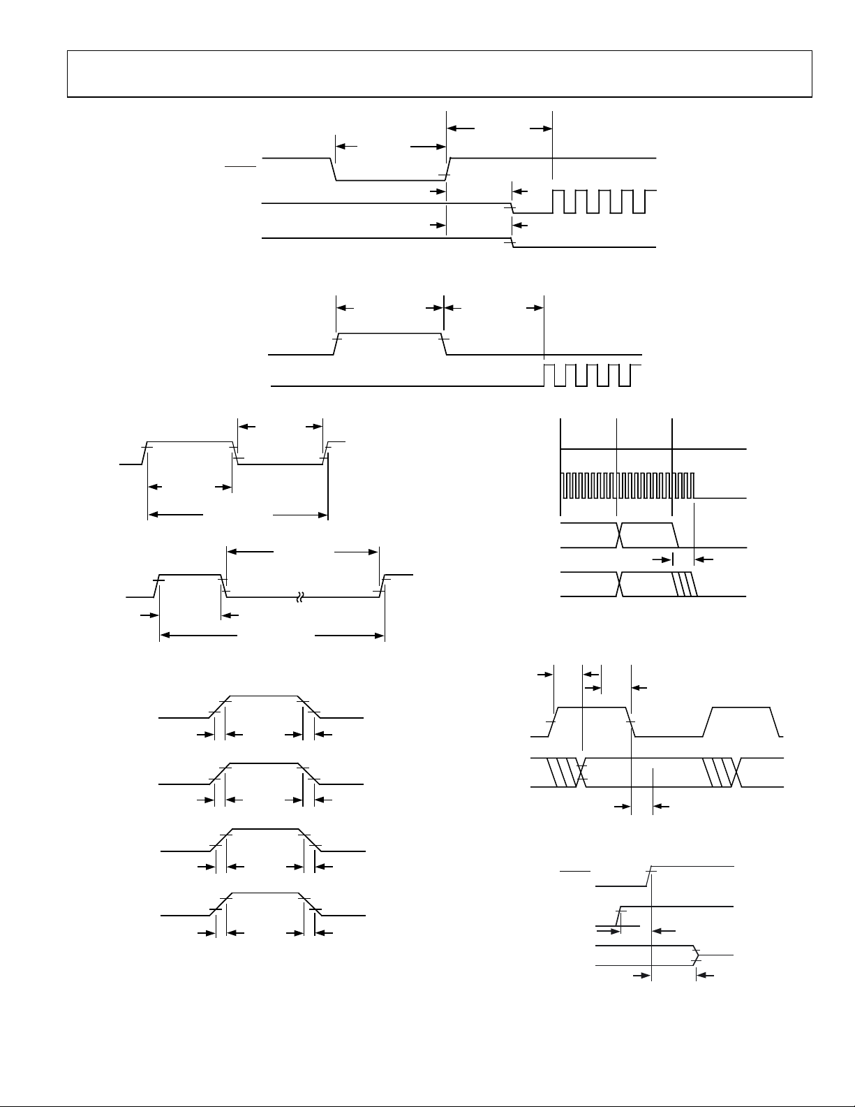
Figure 3. Cold Reset Timing (Codec is Supplying the Bit_CLK Signal)
TRI2ACTV
t
TRI2ACTV
03610-0-003
BIT_CLK
SYNC
SDATA_IN
BIT_CLK
SYNC
t
CLK_HIGH
t
SYNC_HIGH
t
RISECLK
t
RISESYNC
t
RISEDIN
SYNC
BIT_CLK
t
CLK_LOW
t
CLK_PERIOD
t
SYNC_LOW
t
SYNC_PERIOD
Figure 5. Clock Timing
t
SYNC_HIGH
Figure 4. Warm Reset Timing
03610-0-005
t
FALLCLK
t
FALLSYNC
t
FALLDIN
t
SYNC2CLK
BIT_CLK
SDATA_OU
SDATA_IN
SLOT 1 SLOT 2
SYNC
BIT_CLK
SDATA_OU
WRITE TO
03 26
SDATA_IN
BIT_CLK NOT TO SCALE
Figure 7. AC Link Low Power Mode Timing
t
CO
V
IH
SYNC
Figure 8. AC Link Low Power Mode Timing
RESET
V
OH
V
OL
t
HOLD
t
SETUP
03610-0-004
DATA
PR4
V
IL
t
S2_PDOWN
03610-0-007
03610-0-008
SDATA_OUT
SDATA_OUT
t
RISEDOUT
Figure 6. Signal Rise and Fall Times
t
FALLDOUT
03610-0-006
SDATA_IN, BIT_CLK
EAPD, SPDIF_OUT
AND DIGITAL I/O
t
SETUP2RST
t
OFF
Hi-Z
03610-0-009
Figure 9. ATE Test Mode
Rev. A | Page 9 of 48
Page 10
AD1985
ABSOLUTE MAXIMUM RATINGS
Table 15.
Parameter Min Max Unit
POWER SUPPLIES
Digital (DVDD) –0.3 +3.6 V
Analog (AVDD) –0.3 +6.0 V
INPUT CURRENT
(EXCEPT SUPPLY PINS)
ANALOG INPUT VOLTAGE
(SIGNAL PINS)
DIGITAL INPUT VOLTAGE
(SIGNAL PINS)
AMBIENT TEMPERATURE (OPERATING) 0 70 °C
STORAGE TEMPERATURE –65 +150 °C
±10.0 mA
–0.3 AV
–0.3 DV
+ 0.3 V
DD
+ 0.3 V
DD
Stresses above those listed under Absolute Maximum Ratings
may cause permanent damage to the device. This is a stress
rating only; functional operation of the device at these or any
other conditions above those indicated in the operational
section of this specification is not implied. Exposure to absolute
maximum rating conditions for extended periods may affect
device reliability.
ENVIRONMENTAL CONDITIONS
Ambient Temperature Rating
T
CASE
PD = Power Dissipation in W
= Thermal Resistance (Junction to Ambient)
θ
JA
= Thermal Resistance (Junction to Case)
θ
JC
Table 16. Thermal Resistance
Package Type θJA θ
LQFP 50.1°C/W 17.8°C/W
All measurements per EIA/JESD51 with 2S2P test board per EIA/JESD51-7.
= Case Temperature in °C
JC
ESD CAUTION
ESD (electrostatic discharge) sensitive device. Electrostatic charges as high as 4000 V readily accumulate on the
human body and test equipment and can discharge without detection. Although this product features
proprietary ESD protection circuitry, permanent damage may occur on devices subjected to high energy
electrostatic discharges. Therefore, proper ESD precautions are recommended to avoid performance
degradation or loss of functionality.
Rev. A | Page 10 of 48
Page 11
AD1985
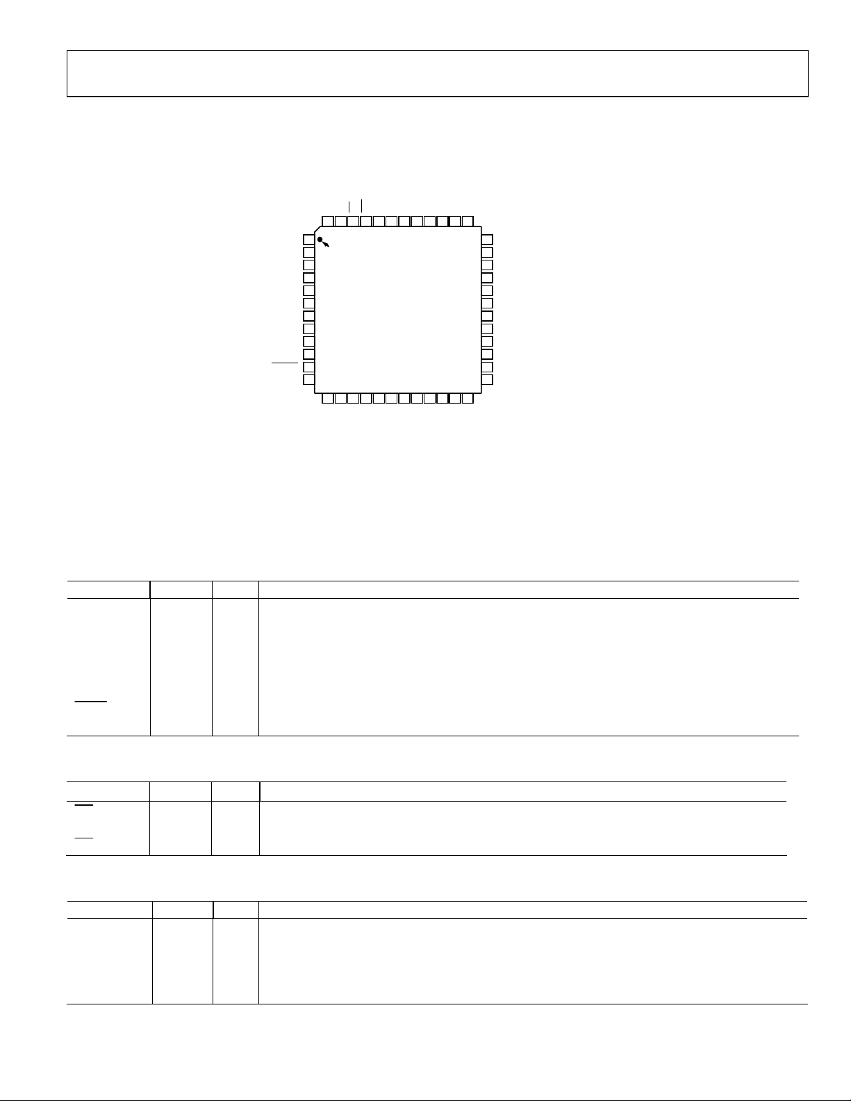
PIN CONFIGURATION AND FUNCTION DESCRIPTIONS
DV
DD1
XTL_IN
XTL_OUT
DV
SS1
SDATA_OUT
BIT_CLK
DV
SS2
SDATA_IN
DV
DD2
SYNC
RESET
JS3
EAPD
ID1
AUX_L
AUX_R
SS3AVDD3
ID0
AV
AD1985
TOP VIEW
(Not to Scale)
JS1
JS0
SPDIF
48 47 46 45 44 39 38 3743 42 41 40
1
PIN 1
2
IDENTIFIER
3
4
5
6
7
8
9
10
11
12
13 14 15 16 17 18 19 20 21 22 23 24
PHONE_IN
SS2
NC
CD_L
CD_GND_REF
DD2
SURR/HP_OUT_R
AV
SURR/HP_OUT_L
AV
MONO_OUT
LINE_OUT_R (FRONT)/SURR_R
36
LINE_OUT_L (FRONT)/SURR_L
35
AV
34
DD4
JS2
33
LFE_OUT
32
CENTER_OUT
31
AFILT2
30
AFILT1
29
V
28
REFOUT
V
27
REF
AV
26
SS1
AV
25
DD1
NC = NO CONNECT
MIC1
MIC2
CD_R
LINE_IN_L
LINE_IN_R
03610-A-011
Figure 10. 48-Lead LQFP Pin Configuration
Circuit Layout Note: In normal operation, Surround and Line Out are swapped to provide headphone drive on line outputs. Therefore, Pins 35 and 36 become the
surround L/R outputs and Pins 39 and 41 become the Line Out (Front) L/R outputs with headphone drive. See Bits LOSEL and HPSEL in Register 0x76 for details.
PIN FUNCTION DESCRIPTIONS
Table 17. Digital I/O
Mnemonic Pin No. I/O Description
XTL_IN 2 I Crystal Input (24.576 MHz) or External Clock In (24.576 MHz, 14.31818 MHz, or 48.000 MHz).
XTL_OUT 3 O Crystal Output.
SDATA_OUT 5 I AC Link Serial Data Output. AD1985 input stream.
BIT_CLK 6 O/I AC Link Bit Clock. 12.288 MHz serial data clock. (Input pin, for secondary mode only.)
SDATA_IN 8 O AC Link Serial Data Input. AD1985 output stream.
SYNC 10 I AC Link Frame Sync.
RESET
SPDIF 48 O SPDIF Output.
Table 18. Chip Selects/Clock Strapping
Mnemonic Pin No. I/O Description
ID0
ID1
11 I AC Link Reset. AD1985 master hardware reset.
45 I
Chip Select Input 0 (Active Low).
This pin can also be used as the chain input from a secondary codec.
46 I Chip Select Input 1 (Active Low).
Table 19. Jack Sense/EAPD
Mnemonic Pin No. Type Description
EAPD 47 O EAPD Output.
JS0 17 I JACK SENSE 0 Input.
JS1 16 I JACK SENSE 1 Input.
JS2 33 I JACK SENSE 2 Input.
JS3 12 I JACK SENSE 3 Input.
Rev. A | Page 11 of 48
Page 12

AD1985
Table 20. Analog I/O
Mnemonic Pin No. I/O Description
PHONE_IN 13 I Monaural Line-Level Input.
AUX_L 14 I Auxiliary Input, Left Channel.
AUX_R 15 I Auxiliary Input, Right Channel.
CD_L 18 I CD Audio Left Channel.
CD_GND_REF 19 I CD Audio Analog Ground Reference for Differential CD Input.
CD_R 20 I CD Audio Right Channel.
MIC1 21 I Microphone 1 Input.
MIC2 22 I Microphone 2 Input.
LINE_IN_L 23 I Line In Left Channel.
LINE_IN_R 24 I Line In Right Channel.
CENTER_OUT 31 I/O Center Channel Output or Input to Recorder (depending on OMS bit in Reg 0x74).
LFE_OUT 32 I/O Low Frequency Enhanced Output or Input to Recorder (depending on OMS bit in Reg 0x74).
LINE_OUT_L/SURR_L 35 O Line Out (Front) Left Channel or Surround Left Channel (depending on LOSEL bit in Reg 0x76).
LINE_OUT_R/SURR_R 36 O Line Out (Front) Right Channel or Surround Right Channel (depending on LOSEL bit in Reg 0x76).
MONO_OUT 37 O Monaural Output to Telephony Subsystem Speakerphone.
SURR_OUT_L/HP_OUT_L 39 O Surround or Front Headphone Left Channel Output (depending on HPSEL bit in Reg 0x76).
SURR_OUT_R/HP_OUT_R 41 O Surround or Front Headphone Right Channel Output (depending on HPSEL bit in Reg 0x76).
Table 21. Filter/Reference
Mnemonic Pin No. I/O Description
V
27 O Voltage Reference Filter.
REF
V
28 O Voltage Reference Output (Intended for Mic Bias).
REFOUT
AFILT1 29 O Antialiasing Filter Capacitor—ADC Right Channel.
AFLIT2 30 O Antialiasing Filter Capacitor—ADC Left Channel.
Table 22. Power and Ground Signals
Mnemonic Pin No. Type Description
DV
1 I Digital VDD: 3.3 V.
DD1
DV
4 I Digital Ground.
SS1
DV
7 I Digital Ground.
SS2
DV
9 I Digital VDD: 3.3 V.
DD2
AV
25 I Analog VDD: 5.0 V.
DD1
AV
26 I Analog Ground.
SS1
AV
34 I Analog VDD: 5.0 V.
DD4
AV
38 I Analog VDD: 5.0 V.
DD2
AV
40 I Analog Ground.
SS2
AV
43 I Analog VDD: 5.0 V.
DD3
AV
44 I Analog Ground.
SS3
Table 23. No Connects
Mnemonic Pin No. Type Description
NC 42 N/A No Connect.
Rev. A | Page 12 of 48
Page 13
AD1985
INDEXED CONTROL REGISTERS
Reg Name D15 D14 D13 D12 D11 D10 D9 D8 D7 D6 D5 D4 D3 D2 D1 D0 Default
0x00 Reset
0x02 Master Volume
0x04 Headphones Volume
0x06 Mono Volume
0x0A PC Beep
0x0C Phone_In Volume
0x0E MIC Volume
0x10 Line In Volume
0x12 CD Volume
0x16 AUX In Volume
0x18 PCM Out Vol
0x1A Record Select
0x1C Record Gain
0x20 General Purpose
0x24 Audio Int. and Paging
0x26 Power-Down Ctrl/Stat
0x28 Extended Audio ID
0x2A Ext’d Audio Stat/Ctrl
0x2C PCM Front DAC Rate
0x2E PCM Surr DAC Rate
0x30 PCM LFE/C DAC Rate
0x32 PCM L/R ADC Rate
0x36 Center/LFE volume
0x38 Surround Volume
0x3A SPDIF Control
0x60 EQ Control
0x62 EQ Data
0x70 J Sense/General
0x72 J Sense/Audio/Status
0x74 Serial Configuration
0x76 Misc Control Bits
0x78 Advanced Jack Sense
0x7C Vendor ID1
0x7E Vendor ID2
0x60
Codec Class/Rev
pg. 1
0x62
PCI SVID
pg. 1
0x64
PCI SID
pg. 1
0x66
Function Select
pg. 1
0x68
Function Information
pg. 1
0x6A
Sense Register
pg. 1
NOTES
Odd register addresses are aliased to the next lower even address.
Registers not shown and bits containing an X are assumed to be reserved.
Reserved registers should not be written. Zeros should be written to reserved bits.
1
For AC ‘97 compatibility, these RM bits must be enabled before they can have any effect.
X SE4 SE3 SE2 SE1 SE0 ID9 ID8 ID7 ID6 ID5 ID4 ID3 ID2 ID1 ID0 0x0090
MM X X LMV4 LMV3 LMV2 LMV1 LMV0 MMRM1 X X RMV4 RMV3 RMV2 RMV1 RMV0 0x8000
HPM X X LHV4 LHV3 LHV2 LHV1 LHV0 HPRM1 X X RHV4 RHV3 RHV2 RHV1 RHV0 0x8000
MVM X X X X X X X X X X MV4 MV2 MV2 MV1 MV0 0x8000
PCBM X X PCBF7 PCBF6 PCBF5 PCBF4 PCBF3 PCBF2 PCBF1 PCBF0 PCBV3 PCBV2 PCBV1 PCBV0 X 0x8000
PHM X X X X X X X X X X PHV4 PHV3 PHV2 PHV1 PHV0 0x8008
MCM X X X X X X X X M20 X MCV4 MCV3 MCV2 MCV1 MCV0 0x8008
LM X X LLV4 LLV3 LLV2 LLV1 LLV0 LVRM1 X X RLV4 RLV3 RLV2 RLV1 RLV0 0x8808
CM X X LCV4 LCV3 LCV2 LCV1 LCV0 CDRM1 X X RCV4 RCV3 RCV2 RCV1 RCV0 0x8808
AM X X LAV4 LAV3 LAV2 LAV1 LAV0 AVRM1 X X RAV4 RAV3 RAV2 RAV1 RAV0 0x8808
OM X X LOV4 LOV3 LOV2 LOV1 LOV0 OMRM1 X X ROV4 ROV3 ROV2 ROV1 ROV0 0x8808
X X X X X LS2 LS1 LS0 X X X X X RS2 RS1 RS0 0x0000
IM X X X LIV3 LIV2 LIV1 LIV0 IMRM1 X X X RIV3 RIV2 RIV1 RIV0 0x8000
X X X X DRSS1 DRSS0 MIX MS LPBK X X X X X X X 0x0000
I4 I3 I2 I1 I0 X X X X X X X PG3 PG2 PG1 PG0 0xXXXX
EAPD PR6 PR5 PR4 PR3 PR2 PR1 PR0 X X X X REF ANL DAC ADC N/A
AID1 AID0 X X REV1 REV0 AMAP AIDLDAC AIDSDAC AIDCDAC DSA1 DSA0 X AIDSPDIF DRA AIDVRA 0xXBC7
VFORCE X PRK PRJ PRI SPCV X ASCLDAC ASCSDAC ASCCDAC SPSA1 SPSA0 X ASCSPDF ASCDRA ASCVRA 0xXXXX
SRF15 SRF14 SRF13 SRF12 SRF11 SRF10 SRF9 SRF8 SRF7 SRF6 SRF5 SRF4 SRF3 SRF2 SRF1 SRF0 0xBB80
SRS15 SRS14 SRS13 SRS12 SRS11 SRS10 SRS9 SRS8 SRS7 SRS6 SRS5 SRS4 SRS3 SRS2 SRS1 SRS0 0xBB80
SRCL15 SRCL14 SRCL13 SRCL12 SRCL11 SRCL10 SRCL9 SRCL8 SRCL7 SRCL6 SRCL5 SRCL4 SRCL3 SRCL2 SRCL1 SRCL0 0xBB80
SRA15 SRA14 SRA13 SRA12 SRA11 SRA10 SRA9 SRA8 SRA7 SRA6 SRA5 SRA4 SRA3 SRA2 SRA1 SRA0 0xBB80
LFEM X X LFE4 LFE3 LFE2 LFE1 LFE0 CNTM X X CNT4 CNT3 CNT2 CNT1 CNT0 0x8080
LSM X LSR5 LSR4 LSR3 LSR2 LSR1 LSR0 RSM X RSR5 RSR4 RSR3 RSR2 RSR1 RSR0 0x8080
AUD
JS1
INT
PRO 0x2000
JS0
N/A
INT
V X SPSR1 SPSR0 L CC6 CC5 CC4 CC3 CC2 CC1 CC0 PRE COPY
EQM X X X X X X X SYM CHS BCA5 BCA4 BCA3 BCA2 BCA1 BCA0 0x8080
CFD15 CFD14 CFD13 CFD12 CFD11 CFD10 CFD9 CFD8 CFD7 CFD6 CFD5 CFD4 CFD3 CFD2 CFD1 CFD0 0x0000
X X X X X X X X MMDIS JS2SEL X X X X X X N/A
JS
JS1
JS0
JS
JS
JS
JS1
JS0
JS1
SPRD
DMX
DMX
MT2
MT1
MT0
EQB
EQB
SLOT16 REGM2 REGM1 REGM0 REGM3 DRF OMS CHEN SPOVR LBKS1 LBKS0 INTS CSWP SPAL SPDZ SPLNK 0x1001
DACZ AC97NC MSPLT LODIS CLDIS HPSEL DMIX1 DMIX0 SPRD 2CMIC LOSEL SRU VREFH VREFD MBG1 MBG0 0x0000
X X X X X X X X JS3TMR JS2TMR JS3MD JS2MD JS3ST JS2ST JS3INT JS2INT N/A
VIDF7 VIDF6 VIDF5 VIDF4 VIDF3 VIDF2 VIDF1 VIDF0 VIDS7 VIDS6 VIDS5 VIDS4 VIDS3 VIDS2 VIDS1 VIDS0 0x4144
VIDT7 VIDT6 VIDT5 VIDT4 VIDT3 VIDT2 VIDT1 VIDT0 VIDREV7 VIDREV6 VIDREV5 VIDREV4 VIDREV3 VIDREV2 VIDREV1 VIDREV0 0x5375
X X X CL4 CL3 CL2 CL1 CL0 RV7 RV6 RV5 RV4 RV3 RV2 RV1 RV0 N/A
PVI15 PVI14 PVI13 PVI12 PVI11 PVI10 PVI9 PVI8 PVI7 PVI6 PVI5 PVI4 PVI3 PVI2 PVI1 PVI0 N/A
PI15 PI14 PI13 PI12 PI11 PI10 PI9 PI8 PI7 PI6 PI5 PI4 PI3 PI2 PI1 PI0 N/A
X X X X X X X X X X X FC3 FC2 FC1 FC0 T/R 0x0000
G4 G3 G2 G1 G0 INV DL4 DL3 DL2 DL1 DL0 IV X X X FIP N/A
ST2 ST1 ST0 S4 S3 S2 S1 S0 OR1 OR0 SR5 SR4 SR3 SR2 SR1 SR0 N/A
TMR
JS0
TMR
JS1
MD
JS0
MD
JS1
ST
JS0
ST
Rev. A | Page 13 of 48
Page 14

AD1985
Reset (Index 0x00)
Reg Num Name D15 D14 D13 D12 D11 D10 D9 D8 D7 D6 D5 D4 D3 D2 D1 D0 Default
0x00 Reset X SE4 SE3 SE2 SE1 SE0 ID9 ID8 ID7 ID6 ID5 ID4 ID3 ID2 ID1 ID0 0x0090
Note: Writing any value to this register performs a register reset, which causes all registers (except Register 0x74) to revert to their default values. Register 0x74 will only
reset Bits CSWP (D3), LBKS[1:0] (D[6:5]), and OMS (D9). The REGM and serial configuration bits are reset only by an external hardware reset.
Reading this register returns the ID code of the part and a code for the type of 3D stereo enhancement.
ID[9:0] Identify Capability: The ID decodes the capabilities of AD1985 based on the following:
Bit = 1 Function AD1985
ID0 Dedicated MIC PCM In Channel 0
ID1 Reserved (per AC ’97, 2.3) 0
ID2 Bass and Treble Control 0
ID3 Simulated Stereo (Mono to Stereo) 0
ID4 Headphone Out Support 1
ID5 Loudness (Bass Boost) Support 0
ID6 18-Bit DAC Resolution 0
ID7 20-Bit DAC Resolution 1
ID8 18-Bit ADC Resolution 0
ID9 20-Bit ADC Resolution 0
SE[4:0] Stereo Enhancement. The AD1985 does not provide hardware 3D stereo enhancement (all bits are 0).
Rev. A | Page 14 of 48
Page 15

AD1985
Master Volume Register (Index 0x02)
Reg Num Name D15 D14 D13 D12 D11 D10 D9 D8 D7 D6 D5 D4 D3 D2 D1 D0 Default
0x02 Master Volume MM X X LMV4 LMV3 LMV2 LMV1 LMV0 MMRM1 X X RMV4 RMV3 RMV2 RMV1 RMV0 0x8000
1
For AC ’97 compatibility, Bit D7 (MMRM) is available only by setting the MSPLT bit in Register 0x76. The MSPLT bit enables separate mute bits for the left and right
channels.
This register controls the LINE_OUT volume and mute bits.
Each volume subregister contains five bits, generating 32
Note that depending on the state of the AC97NC bit in Register
0x76, this register has the following additional functionality:
volume levels with increments of 1.5 dB each.
• For AC97NC = 0, the register controls the LINE_OUT output
AC ’97 defines the 6-bit volume registers, therefore, to maintain
attenuators only.
compatibility whenever the D5 or D13 bit is set to 1, its
respective lower five volume bits are automatically set to 1 by
the codec logic. On readback, all lower five bits will read 1s
• For AC97NC = 1, the register controls the LINE_OUT, center,
and LFE output attenuators.
whenever these bits are set to 1.
RMV[4:0]
Right Master Volume Control. The least significant bit represents 1.5 dB. This register controls the output from
0 dB to a maximum attenuation of 46.5 dB.
MMRM
Right Channel Mute. Once enabled by the MSPLT bit in Register 0x76, this bit mutes the right channel
separately from the MM bit. Otherwise, this bit will always read 0 and will have no effect when set to 1.
LMV[4:0]
Left Master Volume Control. The least significant bit represents 1.5 dB. This register controls the output from
0 dB to a maximum attenuation of 46.5 dB.
MM
Master Volume Mute. When this bit is set to 1, all channels are muted, unless the MSPLT bit in Register 0x76 is
set to 1, in which case, this mute bit will only affect the left channels.
Volume Settings for Master and Headphone
Reg.
0x76
Master Volume (0x02) and Headphone Volume (0x04)
Control Bits
Left Channel Volume D[13:8] Right Channel Volume D[5:0]
MSPLT1
0 0
D15 Write Readback Function D7
00
0000
0 0
00
1111
0 0
01
1111
00 0000 0 dB Gain x
00 1111 –22.5 dB Gain x
01 1111 –46.5 dB Gain x
1
Write Readback Function
00
00 0000 0 dB Gain
0000
00
00 1111 –22.5 dB Gain
1111
01
01 1111 –46.5 dB Gain
1111
0 0 1x xxxx 01 1111 –46.5 dB Gain x 1x xxxx 01 1111 –46.5 dB Gain
0 1 xx xxxx xx xxxx –∞ dB Gain, Muted x xx xxxx xx xxxx –∞ dB Gain, Muted
1 0 1x xxxx 01 1111 –46.5 dB Gain 1 xx xxxx xx xxxx
–∞ dB Gain, Only Right
Muted
1 1 xx xxxx xx xxxx
–∞ dB Gain, Only Left
0 1x xxxx 01 1111 –46.5 dB Gain
Muted
1 1 xx xxxx xx xxxx –∞ dB Gain, Left Muted 1 xx xxxx xx xxxx –∞ dB Gain, Right Muted
Note: x in the above table is a wild card, meaning the value has no effect.
1
For AC ’97 compatibility, Bit D7 is available only by setting the MSPLT bit, Register 0x76. The MSPLT bit enables separate mute bits for the left and right channels. If
MSPLT is not set, Bit D7 has no effect.
Rev. A | Page 15 of 48
Page 16

AD1985
Headphone Volume Register (Index 0x04)
Reg Num Name D15 D14 D13 D12 D11 D10 D9 D8 D7 D6 D5 D4 D3 D2 D1 D0 Default
0x04 Headphones Volume HPM X X LHV4 LHV3 LHV2 LHV1 LHV0 HPRM1X X RHV4 RHV3 RHV2 RHV1 RHV0 0x8000
1
For AC ’97 compatibility, Bit D7 (HPRM) is available only by setting the MSPLT bit in Register 0x76. The MSPLT bit enables separate mute bits for the left and right
channels.
This register controls the headphone volume for both stereo
channels and mute bits. Each volume subregister contains five
bits, generating 32 volume levels with increments of 1.5 dB each.
AC ’97 defines the 6-bit volume registers, therefore, to maintain
compatibility whenever the D5 or D13 bit is set to 1, its
respective lower five volume bits are automatically set to 1 by
the codec logic. On readback, all lower five bits will read 1s
whenever these bits are set to 1 (see the Volume Settings for
Master and Headphone table on the previous page).
Note that depending on the state of the AC97NC bit in Register
0x76, this register has the following additional functionality:
• For AC97NC = 0, the register has no control over the
SURR_OUT/HP_OUT outputs (see Register 0x38).
• For AC97NC = 1, the register controls the
SURR_OUT/HP_OUT output attenuators.
RHV[4:0]
HPRM
LHV[4:0]
HPM
Right Headphone Volume Control.
from 0 dB to a maximum attenuation of 46.5 dB.
Right Channel Mute. Once enabled by the MSPLT bit in Register 0x76, this bit mutes the right channel
separately from the HPM bit. Otherwise, this bit will always read 0 and will have no effect when set to 1.
Left Headphone Volume Control.
from 0 dB to a maximum attenuation of 46.5 dB.
Headphones Volume Mute. When this bit is set to 1, both the left and right channels are muted, unless the
MSPLT bit in Register 0x76 is set to 1, in which case, this mute bit will only affect the left channel.
The least significant bit represents 1.5 dB. This register controls the output
The least significant bit represents 1.5 dB. This register controls the output
Rev. A | Page 16 of 48
Page 17

AD1985
Mono Volume Register (Index 0x06)
Reg Num Name D15 D14 D13 D12 D11 D10 D9 D8 D7 D6 D5 D4 D3 D2 D1 D0 Default
0x06 Mono Volume MVM X X X X X X X X X X MV4 MV3 MV2 MV1 MV0 0x8000
This register controls the mono output volume and mute bit.
The volume register contains five bits, generating 32 volume
levels with increments of 1.5 dB each.
AC ’97 defines the 6-bit volume registers, therefore, to maintain
compatibility whenever the D5 bit is set to 1, its respective lower
five volume bits are automatically set to 1 by the codec logic. On
readback, all lower five bits will read 1s whenever this bit is set
to 1.
MV[4:0]
MVM Mono Volume Mute. When this bit is set to 1, the channel is muted.
Mono Volume Control. The least significant bit represents 1.5 dB. This register controls the output from 0 dB to
a maximum attenuation of 46.5 dB.
Volume Settings for Mono
Control Bits D[4:0] for Mono (0x06)
D15
Write Readback
0 0 0000 0 0000 0 dB Gain
0 0 1111 0 1111 –22.5 dB Gain
0 1 1111 1 1111 –46.5 dB Gain
1 x xxxx x xxxx –∞ dB Gain, Muted
Note that the x in the above table is a wild card, meaning the value has no effect.
Function
Rev. A | Page 17 of 48
Page 18

AD1985
PC Beep Register (Index 0x0A)
Reg Name D15 D14 D13 D12 D11 D10 D9 D8 D7 D6 D5 D4 D3 D2 D1 D0 Default
0x0A PC Beep Volume PCBM X X PCBF7 PCBF6 PCBF5 PCBF4 PCBF3 PCBF2 PCBF1 PCBF0 PCBV3 PCBV2 PCBV1 PCBV0 X 0x8000
This register controls the level and frequency for the digital PC beep generated by the codec. Please note that PC Beep should be muted
when not in use.
PCBV[3:0]
PCBF[7:0]
The register default value is 0x8000, which corresponds to 0 dB attenuation with mute on.
PCBM PV3 to PV0 Function
0 0000 0 dB Attenuation
0 1111 45 dB Attenuation
1 xxxx ∞ dB Attenuation
PCBF Frequency of PC Beep
0x00 PC Beep Disabled
0x01 12 kHz
0x0C 1 kHz
0xFF 47 Hz
Controls the volume of the generated signal. Each step corresponds to approximately 3 dB of attenuation. The
MSB of the register is the mute bit. When this bit is set to 1, the level for the signal is set at –∞ dB.
These bits are writeable, and the codec-digital PC beep generation is supported. The beep frequency generated
is the result of dividing the 48 kHz clock by 4x the number specified in PCBF[7:0], allowing tones from 47 Hz to
12 kHz. A value of 0x00 in Bits PCBF[7:0] disables internal PC beep generation. The PV bits control the volume
level of the generated signal.
Rev. A | Page 18 of 48
Page 19

AD1985
Phone_In Volume Register (Index 0x0C)
Reg Num Name D15 D14 D13 D12 D11 D10 D9 D8 D7 D6 D5 D4 D3 D2 D1 D0 Default
0x0C Phone_In Volume PHM X X X X X X X X X X PHV4 PHV3 PHV2 PHV1 PHV0 0x8008
PHV[4:0]
PHM Phone Mute. When this bit is set to 1, the Phone channel is muted.
Volume Settings for Phone and MIC
Control Bits D[4:0]
Phone (0x0C) and MIC (0x0E)
D15
Write Readback
0 0 0000 0 0000 12 dB Gain
0 0 1000 0 1000 0 dB Gain
0 1 1111 1 1111 –34.5 dB Gain
1 x xxxx x xxxx –∞ dB Gain, Muted
Note that the x in the above table is a wild card, meaning the value has no effect.
Microphone Volume Register (Index 0x0E)
Reg Num Name D15 D14 D13 D12 D11 D10 D9 D8 D7 D6 D5 D4 D3 D2 D1 D0 Default
0x0E MIC Volume MCM X X X X X X X X M20 X MCV4 MCV3 MCV2 MCV1 MCV0 0x8008
This register controls the volume, gain boost, and mute for the gain/attenuators on both the MIC1 and MIC2 paths to the mixer. There is
no separate control for left and right on this path. The signal paths must be identical, hence the single control for both.
Phone Volume. Allows setting the phone volume gain/attenuator to one of 32 levels. The LSB represents 1.5 dB,
and the gain range is +12 dB to –34.5 dB. The default value is 0 dB, with mute bit enabled.
Function
MCV[4:0]
M20
MCM MIC Mute. When this bit is set to 1, both channels are muted.
MIC Volume. Allows setting the MIC volume gain/attenuator to one of 32 levels. The LSB represents 1.5 dB, and the
gain range is +12 dB to –34.5 dB. The default value is 0 dB, with mute enabled.
MIC Gain Boost. This bit allows setting additional MIC gain to increase the microphone sensitivity. Gain is applied
to the microphone path to both the analog mixer and the ADC(s).
The nominal gain boost by default is +20 dB; however, Bits D0 and D1 (MBG[1:0]) on the Miscellaneous Control Bits
Register (0x76), allow changing the gain boost to +10 dB or +30 dB, if necessary.
0 = Disabled; Gain = 0 dB.
1 = Enabled; Default Gain = +20 dB (see Register 0x76, Bits D0 and D1).
Rev. A | Page 19 of 48
Page 20

AD1985
Line In Volume (Index 0x10)
Reg Num Name D15 D14 D13 D12 D11 D10 D9 D8 D7 D6 D5 D4 D3 D2 D1 D0 Default
0x10 Line In Volume LM X X LLV4 LLV3 LLV2 LLV1 LLV0 LVRM1 X X RLV4 RLV3 RLV2 RLV1 RLV0 0x8808
1
For AC ’97 compatibility, Bit D7 (LVRM) is available only by setting the MSPLT bit in Register 0x76. The MSPLT bit enables separate mute bits for the left and right
channels.
RLV[4:0]
LVRM
LLV[4:0]
LM
Volume Settings for Line In, CD Volume, AUX, and PCM Out
Reg. 0x76
MSPLT1
D15 Write Readback Function D7
0 0 0 0000 0 0000 12 dB Gain x 0 0000 0 0000 12 dB Gain
0 0 0 1000 0 1000 0 dB Gain x 0 1000 0 1000 0 dB Gain
0 0 1 1111 1 1111 –34.5 dB Gain x 1 1111 1 1111 –34.5 dB Gain
0 1 x xxxx x xxxx –∞ dB Gain, Muted x x xxxx x xxxx –∞ dB Gain, Muted
1 0 1 1111 1 1111 –34.5 dB Gain 1 x xxxx x xxxx –∞ dB Gain, Only Right Muted
1 1 x xxxx x xxxx –∞ dB Gain, Only Left Muted 0 1 1111 1 1111 –34.5 dB Gain
1 1 x xxxx x xxxx –∞ dB Gain, Left Muted 1 x xxxx x xxxx –∞ dB Gain, Right Muted
1
For AC ’97 compatibility, Bit D7 is available only by setting the MSPLT bit, Register 0x76. The MSPLT bit enables separate mute bits for the left and right channels. If
MSPLT is not set, RM bit has no effect.
Note that the x in the above table is a wild card, meaning the value has no effect.
CD Volume Register (Index 0x12)
Reg Num Name D15 D14 D13 D12 D11 D10 D9 D8 D7 D6 D5 D4 D3 D2 D1 D0 Default
0x12 CD Volume CM X X LCV4 LCV3 LCV2 LCV1 LCV0 CDRM1 X X RCV4 RCV3 RCV2 RCV1 RCV0 0x8808
1
For AC97 compatibility, Bit D7 (CDRM) is available only by setting the MSPLT bit in Register 0x76. The MSPLT bit enables separate mute bits for the left and right
channels. See the Volume Settings for Line In, CD Volume, AUX, and PCM Out table.
RCV[4:0]
CDRM
LCV[4:0]
CM
Right Line In Volume. Allows setting the line in right channel gain/attenuator to one of 32 levels. The LSB
represents 1.5 dB, and the gain range is +12 dB to –34.5 dB. The default value is 0 dB, mute enabled.
Right Channel Mute. Once enabled by the MSPLT bit in Register 0x76, this bit mutes the right channel
separately from the LM bit. Otherwise, this bit will always read 0 and will have no effect when set to 1.
Line In Volume Left. Allows setting the line in left channel gain/attenuator to one of 32 levels. The LSB
represents 1.5 dB, and the gain range is +12 dB to –34.5 dB. The default value is 0 dB, mute enabled.
Line In Mute. When this bit is set to 1, both the left and right channels are muted, unless the MSPLT bit in
Register 0x76 is set to 1, in which case, this mute bit will affect only the left channel.
Control Bits
Line In (0x10), CD (0x12), AUX (0x16), and PCM Out (0x18)
Left Channel Volume D[12:8] Right Channel Volume D[4:0]
1
Write Readback Function
Right CD Volume. Allows setting the CD right channel gain/attenuator to one of 32 levels. The LSB represents
1.5 dB, and the gain range is +12 dB to –34.5 dB. The default value is 0 dB, mute enabled.
Right Channel Mute. Once enabled by the MSPLT bit in Register 0x76, this bit mutes the right channel
separately from the CM bit. Otherwise, this bit will always read 0 and will have no effect when set to 1.
Left CD Volume. Allows setting the CD left channel gain/attenuator to one of 32 levels. The LSB represents
1.5 dB, and the gain range is +12 dB to –34.5 dB. The default value is 0 dB, mute enabled.
CD Volume Mute. When this bit is set to 1, both the left and right channels are muted, unless the MSPLT bit in
Register 0x76 is set to 1, in which case, this mute bit will only affect the left channel.
Rev. A | Page 20 of 48
Page 21

AD1985
AUX In Volume Register (Index 0x16)
Reg Num Name D15 D14 D13 D12 D11 D10 D9 D8 D7 D6 D5 D4 D3 D2 D1 D0 Default
0x16 AUX In Volume AM X X LAV4 LAV3 LAV2 LAV1 LAV0 AVRM1 X X RAV4 RAV3 RAV2 RAV1 RAV0 0x8808
1
For AC ’97 compatibility, Bit D7 (AVRM) is available only by setting the MSPLT bit in Register 0x76. The MSPLT bit enables separate mute bits for the left and right
channels. See the Volume Settings for Line In, CD Volume, AUX, and PCM Out table.
RAV[4:0]
Right AUX Volume. Allows setting the AUX right channel gain/attenuator to one of 32 levels.
dB, and the gain range is +12 dB to –34.5 dB. The default value is 0 dB, mute enabled.
AVRM
Right Channel Mute: Once enabled by the MSPLT bit in Register 0x76, this bit mutes the right channel separately
from the AM bit. Otherwise, this bit will always read 0 and will have no effect when set to 1.
LAV[4:0]
Left AUX Volume. Allows setting the AUX left channel gain/attenuator to one of 32 levels.
1.5 dB, and the gain range is +12 dB to –34.5 dB. The default value is 0 dB, mute enabled.
AM
AUX Volume Mute. When this bit is set to 1, both the left and right channels are muted, unless the MSPLT bit in
Register 0x76 is set to 1, in which case, this mute bit will only affect the left channel.
PCM Out Volume (Index 0x18)
Reg Num Name D15 D14 D13 D12 D11 D10 D9 D8 D7 D6 D5 D4 D3 D2 D1 D0 Default
0x18 PCM Out Vol OM X X LOV4 LOV3 LOV2 LOV1 LOV0 OMRM1 X X ROV4 ROV3 ROV2 ROV1 ROV0 0x8808
1
For AC ’97 compatibility, Bit D7 (OMRM) is available only by setting the MSPLT bit in Register 0x76. The MSPLT bit enables separate mute bits for the left and right
channels. See the Volume Settings for Line In, CD Volume, AUX, and PCM Out table.
Note that depending on the state of the AC97NC bit in Register 0x76, this register has the following additional functionality:
• For AC97NC = 0, the register also controls the surround, center, and LFE DAC gain/attenuators.
• For AC97NC = 1, the register controls the PCM out volume only.
ROV[4:0]
Right PCM Out Volume. Allows setting the PCM right channel gain/attenuator to one of 32 levels. The LSB represents 1.5 dB, and
the gain range is +12 dB to –34.5 dB. The default value is 0 dB, mute enabled.
OMRM
Right Channel Mute. Once enabled by the MSPLT bit in Register 0x76, this bit mutes the right channel separately from the OM
bit. Otherwise, this bit will always read 0 and will have no effect when set to 1.
LOV[4:0]
Left PCM Out Volume. Allows setting the PCM left channel gain/attenuator to one of 32 levels. The LSB represents 1.5 dB, and
the gain range is +12 dB to –34.5 dB. The default value is 0 dB, mute enabled.
OM
PCM Out Volume Mute. When this bit is set to 1, both the left and right channels are muted, unless the MSPLT bit in Register
0x76 is set to 1, in which case, this mute bit will only affect the left channel.
The LSB represents 1.5
The LSB represents
Rev. A | Page 21 of 48
Page 22

AD1985
Record Select Control Register (Index 0x1A)
Reg Num Name D15 D14 D13 D12 D11 D10 D9 D8 D7 D6 D5 D4 D3 D2 D1 D0 Default
0x1A Record Select X X X X X LS2 LS1 LS0 X X X X X RS2 RS1 RS0 0x0000
This register is used to select the record source, independently for the right and left channels.
For single MIC recording, see the MS bit (Register 0x20) for MIC1 and MIC2 input selection.
For dual MIC recording, see the 2CMIC bit (Register 0x76) to enable simultaneous recording into L/R channels.
For output line sharing for the microphones, see the OMS bit (Register 0x74) to swap between the MIC1/MIC2 and C/LFE pins.
The default value is 0x0000, which corresponds to the MIC input for both channels.
RS[2:0] Right Record Select: See table below.
LS[2:0] Left Record Select: See table below.
LS[2:0] Left Record Select
RS[2:0] Right Record Select
OMS 2CMIC MS
0 0 0 MIC1 (mono)
0 0 1 MIC2 (mono)
0 1 0 MIC1 (stereo)
0
0 1 1 MIC2 (stereo)
1 0 0 CENTER (mono)
1 0 1 LFE (mono)
1 1 0 CENTER (stereo)
1 1 1 LFE (stereo)
1 CD_IN (left)
2 Muted
3 AUX_IN (left)
4 LINE_IN (left)
5 Stereo Mix (left)
6 Mono Mix (mono)
7 PHONE_IN (mono)
OMS 2CMIC MS
0 0 0 MIC1 (mono)
0 0 1 MIC2 (mono)
0 1 0 MIC2 (stereo)
0
0 1 1 MIC1 (stereo)
1 0 0 CENTER (mono)
1 0 1 LFE (mono)
1 1 0 LFE (stereo)
1 1 1 CENTER (stereo)
1 CD_IN (right)
2 Muted
3 AUX_IN (right)
4 LINE_IN (right)
5 Stereo Mix (right)
6 Mono Mix (mono)
7 PHONE_IN (mono)
Rev. A | Page 22 of 48
Page 23

AD1985
Record Gain Register (Index 0x1C)
Reg Num Name D15 D14 D13 D12 D11 D10 D9 D8 D7 D6 D5 D4 D3 D2 D1 D0 Default
0x1C Record Gain IM X X X LIV3 LIV2 LIV1 LIV0 IMRM1 X X X RIV3 RIV2 RIV1 RIV0 0x8000
1
For AC ’97 compatibility, Bit D7 (IMRM) is available only by setting the MSPLT bit in Register 0x76. The MSPLT bit enables separate mute bits for the left and right
channels.
RIV[3:0] ADC Right Channel Input Volume Gain Control. Each LSB represents 1.5 dB and the gain range is 0 dB to +22.5 dB.
IMRM
LIV[3:0] ADC Left Channel Input Volume Gain Control. Each LSB represents 1.5 dB and the gain range is 0 dB to +22.5 dB.
IM
IM xIM[3:0] Function
0 1111 +22.5 dB Gain
0 0000 0 dB Gain
1 xxxxx Muted
Right Channel Mute. Once enabled by the MSPLT bit in Register 0x76, this bit mutes the right channel separately
from the IM bit. Otherwise, this bit will always read 0 and will have no effect when set to 1.
Input Mute. When this bit is set to 1, both the left and right channels are muted, unless the MSPLT bit in Register
0x76 is set to 1, in which case, this mute bit will only affect the left channel.
Rev. A | Page 23 of 48
Page 24

AD1985
General Purpose Register (Index 0x20)
Reg Num Name D15 D14 D13 D12 D11 D10 D9 D8 D7 D6 D5 D4 D3 D2 D1 D0 Default
0x20 General Purpose X X X X DRSS1 DRSS0 MIX MS LPBK X X X X X X X 0x0000
LPBK
MS
MIX
DRSS[1:0]
Loopback Control. This bit enables the digital internal loopback from the ADC to the front DAC. This feature is
normally used for testing and troubleshooting. See LBKS bits in Register 0x74 for changing the loopback path to
use the surround or center/LFE DACs.
MIC Select. Selects MIC input into the record selector input and also selects the input to the analog mixer.
(See the 2CMIC [Bit D7 Register 0x76] to enable simultaneous dual microphone recording, and the OMS [Bit D9
Register 0x74] to enable output line sharing for the microphone inputs.)
The following chart shows which of the codec I/O pins are used for the microphone source from the various
settings of the microphone control bits.
OMS 2CMIC MS Left Channel Right Channel
0 0 0 MIC1 (mono) MIC1 (mono)
0 0 1 MIC2 (mono) MIC2 (mono)
0 1 0 MIC1 (stereo) MIC2 (stereo)
0 1 1 MIC2 (stereo) MIC1 (stereo)
1 0 0 CENTER (mono) CENTER (mono)
1 0 1 LFE (mono) LFE (mono)
1 1 0 CENTER (stereo) LFE (stereo)
1 1 1 LFE (stereo) CENTER (stereo)
Mono Output Select. Selects mono output audio source.
0 = Mixer Output. Default.
1 = Selected MIC Channel (Selected Channel Is Unaffected by 2CMIC Setting).
MIX OMS MS Mono Output
0 X X Mixer_mono (default)
1 0 0 MIC1 (mono)
1 0 1 MIC2 (mono)
1 1 0 CENTER (mono)
1 1 1 LFE (mono)
Double Rate Slot Select. The DRSS bits specify the slots for the n + 1 sample outputs. PCM L (n + 1) and
PCM R (n + 1) data are by default provided in output slots 10 and 11.
00: PCM L, R n + 1 data is on slots 10, 11 (reset default).
01: PCM L, R n + 1 data is on slots 7, 8.
10: Reserved.
11: Reserved.
Rev. A | Page 24 of 48
Page 25

AD1985
Audio Interrupt and Paging Mechanism Register (Index 0x24)
Reg Num Name D15 D14 D13 D12 D11 D10 D9 D8 D7 D6 D5 D4 D3 D2 D1 D0 Default
0x24 Audio Int. and Paging I4 I3 I2 I1 I0 X X X X X X X PG3 PG2 PG1 PG0 0xXXXX
Note that this register controls the audio interrupt and register paging mechanisms.
I4 Interrupt Status (Read/Write), Default Is 0.
0: Interrupt is clear.
1: Interrupt was generated.
Interrupt event is cleared by writing a 1 to this bit.
An interrupt in the GPI in Slot 12 in the AC link will follow this bit change when interrupt enable (I0) is unmasked. If this bit is
(I0).
set, one or both of I3 or I2 must be set to indicate the interrupt cause.
I[3:2] Interrupt Cause (Read-Only), Default Is 0.
I[2] = 0: Sense status has not changed (did not cause interrupt).
I[2] = 1: Sense cycle completed or new sense information is available.
I[3] = 0: GPIO status change did not cause interrupt (default)
I[3] = 1: GPIO status change caused interrupt.
These bits will indicate the cause(s) of an interrupt. This information should be used to service the correct interrupting event(s).
the interrupt status bit (I4) is set, one or both of these bits must be set to indicate the interrupt cause.
Hardware resets these bits back to 0 when the interrupt status bit is cleared.
I1 Sense Cycle (Read/Write), Default Is 0.
0: Sense cycle not in progress.
1: Sense cycle start.
Writing a 1 to this bit causes a sense cycle start if supported.
If a sense cycle is in progress, writing a 0 to this bit will abort the sense cycle. The data in the sense result register (0x6A, Page 1)
may or may not be valid, as determined by the IV bit in that register.
I0 Interrupt Enable (Read/Write), Default Is 0.
0: Interrupt generation is masked.
1: Interrupt generation is unmasked.
Software should not unmask the interrupt unless the AC ’97 controller ensures that no conflict is possible with modem Slot 12—
GPI functionality.
AC ’97 2.2 compliant controllers will not likely support audio codec interrupt infrastructure. In that case, software
can poll the interrupt status after initiating a sense cycle and waiting for the Sense Cycle Maximum Delay (which is defined by the
software) to determine if an interrupting event has occurred.
X Reserved.
PG[3:0] Page Selector (Read/Write), Default Is 0x0.
0: Vendor Specific.
0x1: Page ID 01, registers defined in AC’97, Rev. 2.3.
0x2 to 0xF: Reserved Pages.
This register is used to select a descriptor of 16-word pages between Registers 0x60 and 0x6F. A value of 0x0 is used to select
vendor specific space to maintain compatibility with AC ’97 2.2 vendor specific registers.
System software can determine implemented pages by writing the page number and reading the value back.
back does not match the value written, the page is not implemented.
All implemented pages must be in consecutive order, i.e., Page 0x2 cannot be implemented without Page 0x1.
The interrupt status bit will change regardless of the setting of interrupt enable
If
If the value read
Rev. A | Page 25 of 48
Page 26

AD1985
Power-Down Control/Status Register (Index 0x26)
Reg Num Name D15 D14 D13 D12 D11 D10 D9 D8 D7 D6 D5 D4 D3 D2 D1 D0 Default
0x26 Power-Down Ctrl/Stat EAPD PR6 PR5 PR4 PR3 PR2 PR1 PR0 X X X X REF ANL DAC ADC N/A
Note that the ready bits are read-only; writing to REF, ANL, DAC, and ADC will have no effect. These bits indicate the status for the AD1985 subsections. If the bit is a 1,
then that subsection is ready. Ready is defined as the subsection able to perform in its nominal state.
ADC ADC Sections Ready to Transmit Data.
DAC DAC Sections Ready to Accept Data.
ANL Analog Amplifiers, Attenuators, and Mixers Ready.
REF Voltage References, V
PR[6:0] Codec Power-Down Modes. Some bits can be used individually, while others are used in combination.
PR0 ADCs and Input Mux Power-Down. Default setting is 0.
Clearing this bit will enable V
PR1 DACs Power-Down. Also powers down the EQ circuitry. Default setting is 0.
Clearing this bit will enable V
PR2 Mixer Power-Down. Default setting is 0.
PR3 Power Down V
REF
May be used in combination with PR2 or by itself. If all the ADCs and DACs are not powered down, setting this bit will have no
PR4
effect on the V
AC Link Interface Power-Down. Default setting is 0. The reference and the mixer can be either up or down, but all power-up
REF
sequences must be allowed to run to completion before PR5 and PR4 are both set.
In multiple-codec systems, the master codec’s PR4 bit controls the slave codec.
except to enable or disable PR5.
PR5 Internal Clocks Disabled. Default setting is 0.
PR5 has no effect, unless all ADCs, DACs, and the AC link are powered down, e.g., PR0, PR1, PR4.
be either up or down, but all power-up sequences must be allowed to run to completion before PR5 and PR4 are both set. In
multiple codec systems, the master codec’s PR5 controls the slave codec.
is clear.
PR6 Powers Down the Headphone Amplifiers. Default setting is 0.
EAPD External Audio Power-Down Control. Controls the state of the EAPD pin.
EAPD = 0 sets the EAPD pin low, enabling an external power amplifier. (Reset default.)
EAPD = 1 sets the EAPD pin high, shutting the external power amplifier off.
and V
REF
REFOUT
and V
, Up to Nominal Level.
REFOUT
, regardless of the state of PR3.
REF
, regardless of the state of PR3.
REF
. Default setting is 0.
, and it will only power down V
REFOUT
.
In the slave codec, the PR4 bit has no effect,
The reference and the mixer can
PR5 is effective in the slave codec if the master's PR5 bit
NORMAL
PR0 = 1 PR1 = 1 PR2 = 1 PR4 = 1
PR2 = 0
AND
ANL = 1
ANALOG
OFF
PR2 OR
PR3
ADCs OFF
PR0 = 0
AND
ADC = 1
READY = 1
PR0
PR1 = 0
AND
DAC = 1
DACs OFF
PR1
DEFAULT
Figure 11. Example of AC ’97 Power-Down/Power-Up Flow
Rev. A | Page 26 of 48
DIGITAL I/F
OFF
PR4
WARM
RESET
COLD
RESET
SHUT OFF
AC-LINK
Page 27

AD1985
Extended Audio ID Register (Index 0x28)
Reg
Name D15 D14 D13 D12 D11 D10 D9 D8 D7 D6 D5 D4 D3 D2 D1 D0 Default
Num
0x28
Extended
Audio ID
The extended audio ID register identifies which extended audio features are supported. A nonzero extended audio ID value indicates that
one or more of the extended audio features are supported.
AIDVRA
AIDSPDIF SPDIF Support (Read-Only). This bit returns a 1 when read to indicate that SPDIF transmitter is supported (IEC958).
DRA
DSA[1:0]
AIDCDAC PCM Center DAC Support (Read-Only). This bit returns a 1 when read to indicate that PCM Center DAC is supported.
AIDSDAC
AIDLDAC PCM LFE DAC Support (Read-Only). This bit returns a 1 when read to indicate that PCM LFE DAC is supported.
AMAP
REV[1:0] REV[1:0] = 10 Indicates That Codec Is AC ’97 Revision 2.3 Compliant (Read-Only).
AID[1:0] Indicates Codec Configuration (Read-Only).
AID1 AID0 X X REV1 REV0 AMAP AIDLDAC AIDSDAC AIDCDAC DSA1 DSA0 X AIDSPDIF DRA AIDVRA 0xXBC7
Variable Rate PCM Audio Support (Read-Only). This bit returns a 1 when read to indicate that variable rate PCM audio is
supported.
Double Rate Audio (Read-Only). This bit returns a 1 when read to indicate that the optional double rate PCM audio is supported
for PCM L and PCM R.
DAC Slot Assignments. (Read/Write; Reset Default = 00.)
00: DACs 1, 2 = 3 and 4 DACs 3, 4 = 7 and 8 DACs 5, 6 = 6 and 9
01: DACs 1, 2 = 7 and 8 DACs 3, 4 = 6 and 9 DACs 5, 6 = 10 and 11
10: DACs 1, 2 = 6 and 9 DACs 3, 4 = 10 and 11 DACs 5, 6 = 3 and 4
11: DACs 1, 2 = 10 and 11 DACs 3, 4 = 3 and 4 DACs 5, 6 = 7 and 8
PCM Surround DAC Support (Read-Only). This bit returns a 1 when read to indicate that PCM surround left and right DACs are
supported.
Slot DAC Mappings Based on Codec ID (Read-Only). This bit returns a 1 when read to indicate that slot/DAC mappings based on
codec ID is supported.
00 = Primary.
01, 10, 11 = Secondary.
Rev. A | Page 27 of 48
Page 28

AD1985
Extended Audio Status and Control Register (Index 0x2A)
Reg
Name D15 D14 D13 D12 D11 D10 D9 D8 D7 D6 D5 D4 D3 D2 D1 D0 Default
Num
0x2A
Extended
Audio
Stat/Ctrl
The extended audio status and control register is a read/write register that provides status and control of the extended audio features.
ASCVRA Variable Rate Audio (Read/Write).
ASCDRA Double Rate Audio.
ASCSPDF SPDIF Transmitter Subsystem Enable/Disable Bit (Read/Write).
SPSA[1,0] SPDIF Slot Assignment Bits (Read/Write).
ASCCDAC Center DAC Status (Read-Only).
ASCSDAC Surround DAC Status. (Read-only.)
ASCLDAC LFE DAC Status (Read-Only).
SPCV
PRI Center DAC Power-Down (Read/Write).
PRJ Surround DACs Power-Down (Read/Write).
PRK LFE DAC Power-Down (Read/Write).
VFORCE Validity Force Bit. (Reset Default = 0).
VFORCE X PRK PRJ PRI SPCV X ASCLDAC ASCSDAC ASCCDAC SPSA1 SPSA0 X ASCSPDF ASCDRA ASCVRA 0xXXXX
ASCVRA = 0 sets fixed sample rate audio at 48 kHz (reset default).
ASCVRA = 1 enables variable rate audio mode (enables sample rate registers and AC ’97 SLOTREQ signaling).
ASCDRA = 1 enables double-rate audio mode in which data from PCM L and PCM R in output Slots 3 and 4 is used in
conjunction with PCM L (n + 1) and PCM R (n + 1) data to provide DAC streams at twice the sample rate designated by the PCM
Front Sample Rate Control Register.
When using the double rate audio only the front DACs are supported, and all other DACs (surround, center and LFE) are
automatically powered down.
Note that ASCDRA can be used without ASCVRA; in that case, the converter rates are forced to 96 kHz if ASCDRA = 1.
ASCSPDF = 1 enables the SPDIF transmitter.
ASCSPDF = 0 disables the SPDIF transmitter (default).
This bit is also used to validate that the SPDIF transmitter output is actually enabled.
The ASCSPDF bit is only allowed to be set high if the Pin 48 (SPDIF) is pulled down at power-up, enabling the codec transmitter
logic. If the SPDIF pin is floating or pulled high at power-up, the transmitter logic is disabled, and therefore, the ASCSPDF bit
returns a low, indicating that the SPDIF transmitter is not available. This bit must always be read back to verify that the SPDIF
transmitter is actually enabled.
These bits control the SPDIF slot assignment and respective defaults, depending on the codec ID configuration (see the the AC
‘97 2.3 AMAP Compliant Default SPDIF Slot Assignments table for more information.)
ASCCDAC = 1 indicates the PCM center DAC is ready.
ASCSDAC = 1 Indicates the PCM surround DACs are ready.
ASCLDAC = 1 indicates the PCM LFE DAC is ready.
SPDIF Configuration Valid (Read-Only). Indicates the status of the SPDIF transmitter subsystem, enabling the driver to
determine if the currently programmed SPDIF configuration is supported. SPCV is always valid, independent of the SPDIF
enable bit status.
SPCV = 0 indicates current SPDIF configuraton (SPSA, SPSR, DAC slot rate, DRS) is not valid (not supported).
SPCV = 1 indicates current SPDIF configuration (SPSA, SPSR, DAC slot rate, DRS) is valid (is supported).
PRI = 1 mutes the PCM center DAC. Essentially, PRI + PRK = powered off center/LFE DACs.
PRJ = 1 turns off the PCM surround DACs.
PRK = 1 mutes the PCM LFE DAC. Essentially, PRI + PRK = powered off center/LFE DACs.
When asserted, this bit forces the SPDIF stream Validity flag (Bit <28> within each SPDIF L/R subframe) to be controlled by the
V bit (D15) in Register 0x3A (SPDIF control register).
VFORCE = 0 and V = 0: The Validity bit is managed by the codec error detection logic.
VFORCE = 0 and V = 1: The Validity bit is forced high, indicating subframe data is invalid.
VFORCE = 1 and V = 0: The Validity bit is forced low, indicating subframe data is valid.
VFORCE = 1 and V = 1: The Validity bit is forced high, indicating subframe data is invalid.
Rev. A | Page 28 of 48
Page 29

AD1985
AC ‘97 2.3 AMAP Compliant Default SPDIF Slot Assignments
Codec ID Function SPSA = 00 SPSA = 01 SPSA = 10 SPSA = 11
00 2-ch Primary with SPDIF 3 and 4 7 and 8 [default] 6 and 9 10 and 11
00 4-ch Primary with SPDIF 3 and 4 7 and 8 6 and 9 (default) 10 and 11
00 6-ch Primary with SPDIF 3 and 4 7 and 8 6 and 9 10 and 11 (default)
01 +2-ch Secondary with SPDIF 3 and 4 7 and 8 6 and 9 (default)
01 +4-ch Secondary with SPDIF 3 and 4 7 and 8 6 and 9 10 and 11 (default)
10 +2-ch Secondary with SPDIF 3 and 4 7 and 8 6 and 9 (default)
10 +4-ch Secondary with SPDIF 3 and 4 7 and 8 6 and 9 10 and 11 (default)
11 +2-ch Secondary with SPDIF 3 and 4 7 and 8 6 and 9 10 and 11 (default)
PCM Front DAC Rate Register (Index 0x2C)
Reg Num Name D15 D14 D13 D12 D11 D10 D9 D8 D7 D6 D5 D4 D3 D2 D1 D0 Default
0x2C PCM Front DAC Rate SRF15 SRF14 SRF13 SRF12 SRF11 SRF10 SRF9 SRF8 SRF7 SRF6 SRF5 SRF4 SRF3 SRF2 SRF1 SRF0 0xBB80
This read/write sample rate control register contains 16-bit unsigned values, representing the rate of operation in Hz.
SR[15:0]
PCM Surround DAC Rate Register (Index 0x2E)
Reg Num Name D15 D14 D13 D12 D11 D10 D9 D8 D7 D6 D5 D4 D3 D2 D1 D0 Default
0x2E PCM Surr DAC Rate SRS15 SRS14 SRS13 SRS12 SRS11 SRS10 SRS9 SRS8 SRS7 SRS6 SRS5 SRS4 SRS3 SRS2 SRS1 SRS0 0xBB80
This read/write sample rate control register contains 16-bit unsigned values, representing the rate of operation in Hz.
Sample Rate. The sampling frequency range is from 7 kHz (0x1B58) to 48 kHz (0xBB80) in 1 Hz increments. The codec may
not function correctly if frequencies are written outside this range. If 0 is written to ASCVRA (Reg 0x2A), then the sample
rate is reset to 48 kHz.
This register sets the sample rate for the Surround DAC. This register’s reset default is to be locked to the PCM front DAC sample rate
register (0x2C). To unlock this register, Bit SSRU in Register 0x76 must be asserted.
SRS[15:0]
Sample Rate. The sampling frequency range is from 7 kHz (0x1B58) to 48 kHz (0xBB80) in 1 Hz increments. The codec
may not function correctly if frequencies are written outside this range. If 0 is written to ASCVRA (Reg 0x2A), then the
sample rate is reset to 48 kHz.
PCM LFE/Center DAC Rate Register (Index 0x30)
Reg Num NAME D15 D14 D13 D12 D11 D10 D9 D8 D7 D6 D5 D4 D3 D2 D1 D0 Default
0x30 PCM LFE/C DAC
Rate
SRCL15 SRCL14 SRCL13 SRCL12 SRCL11 SRCL10 SRCL9 SRCL8 SRCL7 SRCL6 SRCL5 SRCL4 SRCL3 SRCL2 SRCL1 SRCL0 0xBB80
This read/write sample rate control register contains 16-bit unsigned values, representing the rate of operation in Hz.
This register sets the sample rate for the LFE DAC and center DAC. This register’s reset default is to be locked to the PCM front DAC
sample rate register (0x2C). To unlock this register, Bit SSRU in Register 0x76 must be asserted.
SRCL[15:0]
Sample Rate. The sampling frequency range is from 7 kHz (0x1B58) to 48 kHz (0xBB80) in 1 Hz increments. The codec
may not function correctly if frequencies are written outside this range. If 0 is written to ASCVRA (Register 0x2A), then
the sample rate is reset to 48 kHz.
Rev. A | Page 29 of 48
Page 30

AD1985
PCM L/R ADC Rate Register (Index 0x32)
Reg Num Name D15 D14 D13 D12 D11 D10 D9 D8 D7 D6 D5 D4 D3 D2 D1 D0 Default
0x32 PCM L/R ADC Rate SRA15 SRA14 SRA13 SRA12 SRA11 SRA10 SRA9 SRA8 SRA7 SRA6 SRA5 SRA4 SRA3 SRA2 SRA1 SRA0 0xBB80
This read/write sample rate control register contains 16-bit unsigned values, representing the rate of operation in Hz.
SR[15:0]
Center/LFE Volume Register (Index 0x36)
Reg Num Name D15 D14 D13 D12 D11 D10 D9 D8 D7 D6 D5 D4 D3 D2 D1 D0 Default
0x36 Center/LFE Volume LFEM X X LFE4 LFE3 LFE2 LFE1 LFE0 CNTM X X CNT4 CNT3 CNT2 CNT1 CNT0 0x8080
Sample Rate. The sampling frequency range is from 7 kHz (0x1B58) to 48 kHz (0xBB80) in 1 Hz increments. The codec may
not function correctly if frequencies are written outside this range. If 0 is written to ASCVRA (Register 0x2A), then the
sample rate is reset to 48 kHz.
This register controls the center and LFE output volumes and
mute bits. The volume register contains five bits, generating 32
Note that depending on the state of the AC 97NC bit in
Register 0x76, this register operates as follows:
volume levels with increments of 1.5 dB each.
• For AC'97NC = 0, the register controls the center and LFE
AC ’97 defines the 6-bit volume registers, therefore, to maintain
output pin attenuators. The range is 0 dB to −46.5 dB.
compatibility whenever the D5 or D13 bit is set to 1, its
respective lower five volume bits are automatically set to 1 by
codec logic. On read-back, all lower five bits will read 1s
• For AC97NC = 1, the register controls the center and LFE
DAC gain/attenuators. The range is +12 dB to −34.5 dB.
whenever this bit is set to 1.
CNT[4:0] Center Volume Control.
CNTM Center Volume Mute. When this bit is set to 1, the channel is muted.
LFE[4:0] LFE Volume Control.
LFEM LFE Volume Mute. When this bit is set to 1, the channel is muted.
Note that when the CSWP bit (Register 0x74) is set to 1, the definition of these volume controls for left and right are swapped, i.e., LFE[4:0] and LFEM control center
volume/mute, and CNT[4:0] and CNTM control LFE volume/mute.
CNT/LFE[5:0]
CNTM (LFEM)
0 00 0000 00 0000 0 dB Gain +12 dB Gain
0 00 1111 00 1111 −22.5 dB Gain −10.5 dB Gain
0 01 1111 01 1111 −46.5 dB Gain −34.5 dB Gain
0 1x xxxx 01 1111 −46.5 dB Gain Indeterminate1
1 xx xxxx xx xxxx Muted, −∞ dB Gain Muted, −∞ dB Gain
Note: x in the above table is a wild card, meaning the value has no effect.
Write Readback
Function with AC97NC = 0 Function with AC97NC = 1
1
When AC97NC is set to 1, there is only a 5-bit gain/attenuator to control, so the sixth bit, i.e., the MSB, does not control anything. Therefore, the 5-bit gain setting is
indeterminate, since the five LSBs are listed as wild cards.
Rev. A | Page 30 of 48
Page 31

AD1985
Surround Volume Control Register (Index 0x38)
Reg Num Name D15 D14 D13 D12 D11 D10 D9 D8 D7 D6 D5 D4 D3 D2 D1 D0 Default
0x38 Surround Volume LSM X LSR5 LSR4 LSR3 LSR2 LSR1 LSR0 RSM X RSR5 RSR4 RSR3 RSR2 RSR1 RSR0 0x8080
This register controls the surround volume controls for both
stereo channels and mute bits. Each volume subregister contains
Note that depending on the state of the AC97NC bit in
Register 0x76, this register operates as follows:
five bits, generating 32 volume levels with increments of 1.5 dB
each.
• For AC97NC = 0, the register controls the surround output
pin attenuators. The range is 0 dB to –46.5 dB.
AC ’97 defines the 6-bit volume registers, therefore, to maintain
compatibility whenever the D5 or D13 bit is set to 1, its
respective lower five volume bits are automatically set to 1 by
the codec logic. On read-back, all lower five bits will read 1s
whenever these bits are set to 1.
• For AC97NC = 1, the register controls the surround DAC
gain/attenuators. The range is +12 dB to –34.5 dB.
RSR[5:0] Right Surround Volume Control.
RSM Right Surround Volume Mute. When this bit is set to 1, the right channel is muted.
LSR[5:0] Left Surround Volume Control.
LSM Left Surround Volume Mute. When this bit is set to 1, the left channel is muted.
xSR[5:0]
LSM (RSM)
0 00 0000 00 0000 0 dB Gain +12 dB Gain
0 00 1111 00 1111 −22.5 dB Gain −10.5 dB Gain
0 01 1111 01 1111 −46.5 dB Gain −34.5 Gain
0 1x xxxx 01 1111 −46.5 dB Gain Indeterminate1
1 xx xxxx xx xxxx Muted, −∞ dB Gain Muted, −∞ dB Gain
Note: x in the above table is a wild card, meaning the value has no effect.
Write Readback
Function with AC97NC = 0 Function with AC97NC = 1
1
When AC97NC is set to 1, there is only a 5-bit gain/attenuator to control, so the sixth bit, i.e., the MSB, does not control anything. Therefore, the 5-bit gain setting is
indeterminate, since the five LSBs are listed as wild cards.
Rev. A | Page 31 of 48
Page 32

AD1985
SPDIF Control Register (Index 0x3A)
Reg.Num. Name D15 D14 D13 D12 D11 D10 D9 D8 D7 D6 D5 D4 D3 D2 D1 D0 Default
0x3A SPDIF Control V X SPSR1 SPSR0 L CC6 CC5 CC4 CC3 CC2 CC1 CC0 PRE COPY
AUD
PRO 0x2000
Register 0x3A is a read/write register that controls SPDIF
functionality and manages bit fields propagated as channel
status (or subframe in the V case). With the exception of V, this
register should only be written to when the SPDIF transmitter is
disabled (SPDIF bit in Register 0x2A is 0). This ensures that
control and status information initialize correctly at the
beginning of SPDIF transmission.
PRO Professional. 1 indicates professional use of channel status, 0 indicates consumer.
AUD
Nonaudio. 1 indicates data is nonPCM format, 0 indicates data is PCM.
COPY Copyright. 1 indicates copyright is asserted, 0 indicates copyright is not asserted.
PRE
CC[6:0] Category Code. Programmed according to IEC standards, or as appropriate.
L Generation Level. Programmed according to IEC standards, or as appropriate.
SPSR[1:0]
V
Pre-emphasis. 1 indicates filter pre-emphasis is 50/15 µs, 0 indicates no pre-emphasis.
SPDIF Transmit Sample Rate.
SPSR[1:0] = 00: Transmit Sample Rate = 44.1 kHz.
SPSR[1:0] = 01: Reserved.
SPSR[1:0] = 10: Transmit Sample Rate = 48 kHz (default).
SPSR[1:0] = 11: Not supported.
Validity. This bit affects the Validity flag (Bit <28> transmitted in each SPDIF L/R subframe) and enables the
SPDIF transmitter to maintain connection during error or mute conditions.
V = 1: Each SPDIF subframe (L+R) has Bit <28> set to 1. This tags both samples as invalid.
V = 0: Each SPDIF subframe (L+R) has Bit <28> set to 0 for valid data and 1 for invalid data (error condition).
Note that when V = 0, asserting the VFORCE bit (D15) in Register 0x2A (Extended Audio Stat/Ctrl) will force
the Validity flag low, marking both samples as valid.
Rev. A | Page 32 of 48
Page 33

AD1985
EQ Control Register (Index 0x60)
Reg.Num. Name D15 D14 D13 D12 D11 D10 D9 D8 D7 D6 D5 D4 D3 D2 D1 D0 Default
0x60 EQ Control EQM X X X X X X X SYM CHS BCA5 BCA4 BCA3 BCA2 BCA1 BCA0 0x8080
Register 0x60 is a read/write register that controls equalizer
function and data setup. The register also contains the biquad
and coefficient address pointer, which is used in conjunction
with the EQ data register (0x78) to set up the equalizer
coefficients. The reset default disables the equalizer function
BCA[5:0] Biquad and Coefficient Address Pointer:
biquad 0 coef a0 BCA[5:0] = 011011
biquad 0 coef a1 BCA[5:0] = 011010
biquad 0 coef a2 BCA[5:0] = 011001
biquad 0 coef b1 BCA[5:0] = 011101
biquad 0 coef b2 BCA[5:0] = 011100
biquad 1 coef a0 BCA[5:0] = 100000
biquad 1 coef a1 BCA[5:0] = 011111
biquad 1 coef a2 BCA[5:0] = 011110
biquad 1 coef b1 BCA[5:0] = 100010
biquad 1 coef b2 BCA[5:0] = 100001
biquad 2 coef a0 BCA[5:0] = 100101
biquad 2 coef a1 BCA[5:0] = 100100
biquad 2 coef a2 BCA[5:0] = 100011
biquad 2 coef b1 BCA[5:0] = 100111
biquad 2 coef b2 BCA[5:0] = 100110
biquad 3 coef a0 BCA[5:0] = 101010
biquad 3 coef a1 BCA[5:0] = 101001
biquad 3 coef a2 BCA[5:0] = 101000
biquad 3 coef b1 BCA[5:0] = 101100
biquad 3 coef b2 BCA[5:0] = 101011
biquad 4 coef a0 BCA[5:0] = 101111
biquad 4 coef a1 BCA[5:0] = 101110
biquad 4 coef a2 BCA[5:0] = 101101
biquad 4 coef b1 BCA[5:0] = 110001
biquad 4 coef b2 BCA[5:0] = 110000
biquad 5 coef a0 BCA[5:0] = 110100
biquad 5 coef a1 BCA[5:0] = 110011
biquad 5 coef a2 BCA[5:0] = 110010
biquad 5 coef b1 BCA[5:0] = 110110
biquad 5 coef b2 BCA[5:0] = 110101
biquad 6 coef a0 BCA[5:0] = 111001
biquad 6 coef a1 BCA[5:0] = 111000
biquad 6 coef a2 BCA[5:0] = 110111
biquad 6 coef b1 BCA[5:0] = 111011
biquad 6 coef b2 BCA[5:0] = 111010
CHS Channel Select. CHS = 0: Selects left channel coefficients data block. CHS = 1: Selects right channel coefficients data block.
SYM
EQM
Symmetry. When set to 1 this bit indicates that the left and right channel coefficients are equal. This shortens the coefficient
setup sequence since only the left channel coefficients need to be addressed and set up. (The right channel coefficients are
simultaneously copied into memory.)
Equalizer Mute. When set to 1, this bit disables the equalizer function (allows all data to pass through). The reset default sets this
bit to 1, disabling the equalizer function until the biquad coefficients can be properly set.
until the coefficients can be properly set up by the software and
sets the symmetry bit to allow equal coefficients for left and
right channels.
Rev. A | Page 33 of 48
Page 34

AD1985
EQ Data Register (Index 0x62)
Reg.Num. Name D15 D14 D13 D12 D11 D10 D9 D8 D7 D6 D5 D4 D3 D2 D1 D0 Default
0x62 EQ Data CFD15 CFD14 CFD13 CFD12 CFD11 CFD10 CFD9 CFD8 CFD7 CFD6 CFD5 CFD4 CFD3 CFD2 CFD1 CFD0 0x0000
This read/write register is used to transfer EQ biquad coefficients into memory.
The register data is transferred to, or retrieved from, the address pointed to by the BCA bits in the EQ control register (0x60).
Data will be written to memory only if the EQM bit (Register 0x60, Bit 15) is asserted.
CFD[15:0]
Coefficient Data. The biquad coefficients are fixed-point format values with 16 bits of resolution. The CFD15 bit is the MSB
and the CFD0 bit is the LSB.
Rev. A | Page 34 of 48
Page 35

AD1985
Jack Sense/General Register (Index 0x70)
Reg Num Name D15 D14 D13 D12 D11 D10 D9 D8 D7 D6 D5 D4 D3 D2 D1 D0 Default
0x70 J Sense/General X X X X X X X X MMDIS JS2SEL X X X X X X N/A
JS2SEL Selects JS2 Input Behavior.
0: Standard operation for JS2 jack sensing (default).
1: Enable microphone input sensing with JS2.
MMDIS Mono Mute Disable.
0: Use JSMT[2:0] (Register 0x72) to determine mono out operation (default).
1: Independent of the settings in the JSMT table, this ensures mono out remains active all the time.
X Reserved, Do Not Read/Write These Bits.
Rev. A | Page 35 of 48
Page 36

AD1985
Jack Sense/Audio Interrupt/Status Register (Index 0x72)
Reg
Num Name D15 D14 D13 D12 D11 D10 D9 D8 D7 D6 D5 D4 D3 D2 D1 D0 Default
0x72
Jack Sense/
Audio/Status
Note: All register bits are read/write except for JS0ST and JS1ST, which are read-only.
JS
SPRD
JS1
DMX
JS0
DMX
JS
MT2
JS
MT1
JS
MT0
JS1
EQB
JS0
EQB
JS1
TMR
JS0
TMR
JS1
MD
JS0
MD
JS1
ST
JS0INT
JS1INT
JS0ST JS0 State. This bit always reports the logic state of the JS0 pin.
JS1ST JS1 State. This bit always reports the logic state of the JS1 pin.
JS0MD
JS1MD
JS0TMR JS0 Timer Enable. If this bit is set to a 1, JS0 must be high for greater than 298 ms to be recognized.
JS1TMR JS1 Timer Enable. If this bit is set to a 1, JS1 must be high for greater than 298 ms to be recognized.
JS0EQB
JS1EQB
JSMT[2:0]
JS0DMX
JS1DMX
JSSPRD
Indicates Pin JS0 has generated an interrupt. Remains set until the software services the JS0 interrupt; i.e., JS0 ISR (Interrupt
Service Routine) should clear this bit by writing a 0 to it.
Notes:
1) Interrupts are generated by valid state changes of JS pins.
2) Interrupt to the system is actually an OR combination of this bit and JS3INT to JS0INT.
3) The interrupt implementation path is selected by the INTS bit (Register 0x74).
4) It is also possible to generate a software system interrupt by writing a 1 to this bit.
Indicates Pin JS1 has generated an interrupt. Remains set until the software services the JS1 interrupt; i.e., JS1 ISR (Interrupt
Service Routine) should clear this bit by writing a 0 to it. See JS0INT description above for additional details.
Cannot be used for MIC sensing.
Cannot be used for MIC sensing.
JS0 Mode. This bit selects the operation mode for the JS0 pin.
0: Jack Sense Mode (Reset Default).
1: Interrupt Mode.
JS1 Mode: This bit selects the operation mode for the JS1 pin.
0: Jack Sense Mode (Reset Default).
1: Interrupt Mode.
JS0 EQ Bypass Enable. This bit enables JS0 to control the EQ bypass.
When this bit is set to 1, JS0 = 1 will cause the EQ to be bypassed. Default is 0.
JS1 EQ Bypass Enable. This bit enables JS1 to control the EQ bypass.
When this bit is set to 1, JS1 = 1 will cause the EQ to be bypassed. Default is 0.
JS Mute Enable Selector. These three bits select and enable the jack sense muting action (see theJack Sense Mute Select (JSMT
[2:0]) table).
JS0 Down-Mix Control Enable. This bit enables JS0 to control the down-mix function. This function allows a digital mix of
6-channel audio into 2-channel audio. The mix can then be routed to the stereo LINE_OUT or HP_OUT jacks. When this bit is set
to 1, JS0 = 1 will activate the down-mix conversion.
See the DMIX description in Register 0x76. The DMIX bits select the down-mix implementation type and can also force the
function to be activated.
JS1 Down-Mix Control Enable. This bit enables JS1 to control the down-mix function (see the JS0DMX description).
When this bit is set to 1, JS1 = 1 will activate the down-mix conversion.
JS Spread Control Enable. This bit enables 2-channel to 6-channel audio spread function when both jack senses are active
(Logic State 1). Note that the SPRD bit can also force the spread function without being gated by the jack senses. See this bit’s
description in Register 0x76 for more details on the spread function.
JS0
ST
JS1
INT
JS0
INT
N/A
Rev. A | Page 36 of 48
Page 37

AD1985
Jack Sense Mute Select (JSMT [2:0])
HP
REF JS1 JS0 JSMT2 JSMT1 JSMT0
0 OUT (0) OUT (0) 0 0 0 ACTIVE ACTIVE ACTIVE ACTIVE
1 OUT (0) IN (1) 0 0 0 ACTIVE ACTIVE ACTIVE ACTIVE
2 IN (1) OUT (0) 0 0 0 ACTIVE ACTIVE ACTIVE ACTIVE
3 IN (1) IN (1) 0 0 0 ACTIVE ACTIVE ACTIVE ACTIVE
4 OUT (0) OUT (0) 0 0 1 ACTIVE FMUTE FMUTE ACTIVE
5 OUT (0) IN (1) 0 0 1 ACTIVE FMUTE FMUTE ACTIVE
6 IN (1) OUT (0) 0 0 1 ACTIVE ACTIVE ACTIVE FMUTE
7 IN (1) IN (1) 0 0 1 ACTIVE ACTIVE ACTIVE FMUTE
8 OUT (0) OUT (0) 0 1 0 FMUTE ACTIVE FMUTE ACTIVE
9 OUT (0) IN (1) 0 1 0 FMUTE ACTIVE FMUTE ACTIVE
10 IN (1) OUT (0) 0 1 0 ACTIVE ACTIVE ACTIVE FMUTE
11 IN (1) IN (1) 0 1 0 ACTIVE ACTIVE ACTIVE FMUTE
12 OUT (0) OUT (0) 0 1 1
13 OUT (0) IN (1) 0 1 1
14 IN (1) OUT (0) 0 1 1
15 IN (1) IN (1) 0 1 1
16 OUT (0) OUT (0) 1 0 0 ACTIVE FMUTE FMUTE ACTIVE
17 OUT (0) IN (1) 1 0 0 ACTIVE ACTIVE ACTIVE FMUTE
18 IN (1) OUT (0) 1 0 0 ACTIVE FMUTE FMUTE FMUTE
19 IN (1) IN (1) 1 0 0 ACTIVE FMUTE FMUTE FMUTE
20 OUT (0) OUT (0) 1 0 1 FMUTE FMUTE FMUTE ACTIVE
21 OUT (0) IN (1) 1 0 1 FMUTE FMUTE FMUTE ACTIVE
22 IN (1) OUT (0) 1 0 1 ACTIVE ACTIVE ACTIVE FMUTE
23 IN (1) IN (1) 1 0 1 ACTIVE ACTIVE ACTIVE FMUTE
24 OUT (0) OUT (0) 1 1 0
25 OUT (0) IN (1) 1 1 0
26 IN (1) OUT (0) 1 1 0
27 IN (1) IN (1) 1 1 0
28 OUT (0) OUT (0) 1 1 1
29 OUT (0) IN (1) 1 1 1
30 IN (1) OUT (0) 1 1 1
31 IN (1) IN (1) 1 1 1
FMUTE = Output is forced to mute independent of the respective volume register setting.
ACTIVE = Output is not muted and its status is dependent on the respective volume register setting.
OUT = Nothing is plugged into the jack, and therefore, the JS status is 0 (via the load resistor pull-down action).
IN = Jack has plug inserted, and therefore, the JS status is 1 (via the codec JS pin internal pull-up).
Note: MMDIS (Register 0x70, Bit D7) set to 1 will keep mono out enabled for all the settings above.
OUT
** ** ** **
** ** ** **
** ** ** **
** ** ** **
** ** ** **
** ** ** **
** ** ** **
** ** ** **
** ** ** **
** ** ** **
** ** ** **
** ** ** **
LINE
OUT
C/LFE
OUT
MONO
OUT NOTES
JS0 and JS1 Ignored.
JS0 No Mute Action,
JS1 Mutes Mono and Enables LINE_OUT + C/LFE.
Standard 6-Channel Configuration. Swapped
HP_OUT and LINE_OUT.
JS0 No Mute Action,
JS1 Mutes Mono and Enables HP_OUT and C/LFE.
Standard 6-Channel Configuration. No Swap.
** Reserved.
JS0 = 0 and JS1 = 0 Enables Mono.
JS1 = 1 Enables Front Only.
JS0 = 1 and JS1 = 0 Enables All Rear.
6-Channel Configuration with Front Jack Wrap-Back.
JS0 No Mute Action,
JS1 Mutes Mono and Enables LINE_OUT and HP_OUT
and C/LFE.
Standard 6-Channel Configuration. Swapped
HP_OUT and LINE_OUT.
** Reserved.
** Reserved.
Rev. A | Page 37 of 48
Page 38

AD1985
Serial Configuration (Index 0x74)
Reg
Num Name D15 D14 D13 D12 D11 D10 D9 D8 D7 D6 D5 D4 D3 D2 D1 D0 Default
0x74
Note: This register will only reset bits CSWP (D3), LBKS[1:0] (D[6:5]), and OMS (D9) when Register 0x00 is written to (soft reset). All bits are reset on a hard or hardware
reset.
Serial
Config.
SPLNK SPDIF Link. This bit enables the SPDIF to link with the front DACs for data requesting.
SPDZ SPDIF DACZ.
SPAL SPDIF ADC Loop-Around.
CSWP
INTS Interrupt Mode Select. This bit selects the audio interrupt implementation path.
SLOT16 REGM2 REGM1 REGM0 REGM3 DRF OMS CHEN SPOVR LBKS1 LBKS0 INTS CSWP SPAL SPDZ SPLNK 0x1001
0: SPDIF and front DACs are not linked.
1: SPDIF and front DACs are linked and receive same data requests. (Reset default.)
0: Repeat last sample out the SPDIF stream if FIFO underruns. (Reset default.)
1: Forces midscale sample out the SPDIF stream if FIFO underruns.
0: SPDIF transmitter is connected to the AC Link stream. (Reset default.)
1: SPDIF transmitter is connected to the digital ADC stream, not the AC Link.
Swap the Center/LFE Channels. Some systems have a swapped external connection for the center and LFE Channels.
Setting this bit will swap these channels internal to the codec. Setting this bit also swaps the definitions of the center/LFE
volume controls in Register 0x36.
0: Slot 12, Bit 0 (modem interrupt) (reset default).
1: Slot 6, Valid Bit (MIC ADC interrupt).
Note: This bit does not generate an interrupt. Rather, it steers the path of the generated interrupt.
LBKS[1:0] Loop-Back Selection. These bits select the internal digital loop-back path when the LPBK bit is active (see Register 0x20).
00: Loop back through the front DACs. (Reset default.)
01: Loop back through the surround DACs.
11: Loop back through the center and LFE DACs. (Center DAC loops back from the ADC left channel, the LFE DAC from the
ADC right channel.)
10: Reserved.
SPOVR SPDIF Override.
0: SPDIF Transmitter is enabled only if the SPDIF pin is pulled low on reset. (Reset default.)
1: SPDIF Transmitter is enabled regardless of the SPDIF pin configuration.
CHEN
OMS
DRF DAC Request Force: This allows the AD1985 to synchronize DAC requests with the AD1981A/ AD1981B.
REGM3 Slave 3 Codec Register Mask.
REGM0 Master Codec Register Mask. (Reset default.)
REGM1 Slave 1 Codec Register Mask.
REGM2 Slave 2 Codec Register Mask.
SLOT16
Chain Enable. This bit enables chaining of a slave codec SDATA_IN stream into the
0: Disable chaining. (Reset default.)
1: Enable chaining into
Output Microphone Select. This bit will switch the microphone inputs between the MIC1/MIC2 pins and the Center/LFE
pins. This feature is used for those systems that have input/output jack sharing.
Note: See the charts describing the microphone inputs—the description of MS (Bit D8, Register 0x20) and the record
select control register (0x1A).
0: Microphone inputs come from MIC1 and MIC2 pins. Center/LFE outputs behave as expected (default).
1: Microphone inputs now come from the Center/LFE pins. The codec will place the Center/LFE outputs into a High-Z
state—equivalent to setting CLDIS (Bit D11, Register 0x76). Setting the OMS bit, however, will not overwrite the CLDIS;
Center/LFE outputs respond equally to both bits.
0: Normal DAC requesting sequence. (Reset default.)
1: Synchronize to AD1981A/B DAC requests.
Enable 16-Bit Slot Mode. SLOT16 makes all AC Link slots 16 bits in length, formatted into 16 slots. This is a preferred mode
for DSP serial port interfacing.
ID0
pin.
ID0
pin (Pin 45).
Rev. A | Page 38 of 48
Page 39

AD1985
Miscellaneous Control Bits (Index 0x76)
Reg
Num Name D15 D14 D13 D12 D11 D10 D9 D8 D7 D6 D5 D4 D3 D2 D1 D0 Default
0x76
Misc
Control Bits
MBG[1:0]
VREFD, VREFH
SRU Sample Rate Unlock. Controls all DAC sample rate locking.
LOSEL
2CMIC
SPRD
DACZ AC97NC MSPLT LODIS CLDIS HPSEL DMIX1 DMIX0 SPRD 2CMIC LOSEL SRU VREFH VREFD MBG1 MBG0 0x0000
MIC Boost Gain Select Register. These two bits allow changing both MIC preamp gain blocks from the nominal +20 dB
gain boost. Both MIC1 and MIC2 preamps will be set to the same selected gain.
Note: This gain setting only takes effect while Bit D6 (M20) on the MIC volume register (0x0E) is set to 1, otherwise, the MIC
boost blocks have a gain of 0 dB.
00: +20 dB gain. (Reset default.)
01: +10 dB gain.
10: +30 dB gain.
11: Reserved.
Controls the Level of the V
VREFH VREFD
0 0 2.25 V (Default)
0 1 High-Z
1 0 3.7 V
1 1 0 V
0: All DAC sample rates are locked to the front sample rate. (Reset default.)
1: DAC sample rates can be set independently for front, surround, and LFE.
LINE_OUT Amplifiers Input Select. This bit allows the LINE_OUT output amplifiers to be driven by the mixer or the
surround DACs. The main purpose for this is to allow swapping of the front and surround channels to make better use of
the SURR/HP_OUT output amplifiers. This bit should normally be used in tandem with the HPSEL bit (see below).
0: LINE_OUT amplifiers are driven by the mixer outputs. (Reset default.)
1: LINE_OUT amplifiers are driven by the surround DAC outputs.
2-Channel MIC Select. This bit enables simultaneous recording from MIC1 and MIC2 inputs, using a stereo microphone
array. Note that this register works in conjunction with the MS and OMS bits.
0: MIC1 or MIC2 (determined by MS bit) is routed to the mixer/record selector’s left and right MIC channels. (Reset default.)
1: MIC1 is routed to the mixer/record selector’s left MIC channel, and MIC2 is routed to the mixer/record selector’s right
MIC channel. The MS bit will swap the MIC1/MIC2 left and right assignments.
The OMS bit will select from the MIC1/MIC2 or Center/LFE pins as the input source for the microphone. See the Record
Selector (Register 0x1A), MS bit (Bit D8, Register 0x20), or OMS bit (Bit D9, Register 0x74) definitions for more information.
Spread Enable. This bit enables spreading of 2-channel media to all six output channels. This function is implemented in
the analog section by using the output selector control lines for the center/LFE, surround, and LINE_OUT output channels.
Note that the jack sense pins can also be set up to control (gate) this function depending on the JS1SPRD bit (see
Register 0x72).
0: No Spreading occurs, unless activated by the jack senses and JS1SPRD bit. (Reset default.)
1: The SPRD selector drives the center and LFE outputs from the MONO_OUT, the HPSEL selector drives the SURR/HP_OUT
outputs from the mixer outputs, and the LOSEL selector drives the LINE_OUT outputs from the mixer outputs.
Note that the SPRD bit overrides the current output selector control lines, set up by Bits LOSEL and HPSEL as follows:
LOSEL = 0 and HPSEL = 1.
Pin as Follows:
REFOUT
Rev. A | Page 39 of 48
Page 40

AD1985
DMIX[1:0]
HPSEL
CLDIS
LODIS
MSPLT
AC97NC
DACZ DAC Zero-Fill. Determines DAC data fill under starved condition.
Down-Mix Mode Select. Provides analog down-mixing of the center, LFE, and/or surround channels into the mixer
channels. This allows the full content of 5.1 or quad media to be played through stereo headphones or speakers.
Note that the jack sense pins can also be set up to control (gate) this function depending on the JS0DMX and JS1DMX bits
(see Register 0x72).
The upper bit allows forcing the down-mix function:
DMIX[1] = 0: No down-mix unless activated by the jack senses and JSxDMX bits. (Default.)
DMIX[1] = 1: Forces down-mix function.
The lower bit selects the down-mix type:
DMIX[0] = 0: Selects 6-to-4 down-mix. The center and LFE channels are summed equally into the mixer L/R channels.
(Default.)
DMIX[0] = 1: Selects 6-to-2 down-mix. The surround L/R channels are summed into the mixer L/R channels. The center and
LFE are summed equally into the mixer left and right channels.
Default for DMIX[1:0] is 00.
Headphone Amplifier Input Select. This bit allows the headphone power amps to be driven from the surround DACs or
from the mixer outputs. There are two reasons for this, one is to allow 2-channel media to use the higher power
headphone amplifiers available on the SURR/HP_OUT outputs, and the other is to allow spreading of 2-channel media to
the surround outputs.
Together with the LOSEL bit (see above), this bit also provides for analog swapping of the mixer (front) and surround
outputs.
0: SURR_OUT/HP_OUT outputs are driven by the surround DACs. (Reset default.)
1: SURR_OUT/HP_OUT outputs are driven by the mixer outputs.
Center and LFE Disable: Disables the center and LFE output pins, placing them into High-Z (approximately 30 kΩ
impedance) mode so that the assigned output audio jacks can be shared for MIC inputs or other functions.
0: Center and LFE output pins have normal audio drive capability. (Reset default.)
1: Center and LFE output pins are placed into High-Z mode.
LINE_OUT Disable: Disables the LINE_OUT pins (L/R), placing them into High-Z (approximately 30 kΩ impedance) mode so
that the assigned output audio jack can be shared for Line Input function.
0: LINE_OUT pins have normal audio drive capability. (Reset default.)
1: LINE_OUT pins are placed into High-Z mode.
Mute Split. Allows separate mute control bits for left and right channels in master, HP, LINE_IN, CD, PCM OUT, and record
volume/gain control registers.
0: Both left and right channel mutes are controlled by Bit D15 in their respective registers. (Reset default.)
1: Bit D15 affects only the left channel mute and Bit D7 affects only the right channel mute.
AC ’97 No Compatibility Mode. Changing this bit allows the surround, center, and LFE volume control registers and output
attenuators to operate in a more functional mode than what’s defined by the AC ’97 spec. This is called ADI compatibility
mode.
In AC ’97 compatibility mode, the DAC gain/attenuators for the surround, center, and LFE are controlled by Register 0x18
(PCM volume). The output pin attenuators for the surround are controlled by Register 0x38 and the output pin attenuators
for the center and LFE are controlled by Register 0x36.
In ADI compatibility mode, the surround DAC gain/attenuators are controlled by Register 0x38 and the center/LFE DAC
gain/attenuators are controlled by Register 0x36. The output pin attenuators for the surround, center, and LFE are
controlled by Register 0x02 (master volume).
0: AC ’97 compatibility mode. (Reset default.)
1: ADI compatibility mode.
0: DAC data is repeated when DACs are starved for data. (Reset default.)
1: DAC data is zero-filled when DACs are starved for data.
Rev. A | Page 40 of 48
Page 41

AD1985
Advanced Jack Sense Register (Index 0x78)
Reg Num Name D15 D14 D13 D12 D11 D10 D9 D8 D7 D6 D5 D4 D3 D2 D1 D0 Default
0x78
Advanced
Jack Sense
Note: All register bits are read/write except for JS2ST and JS3ST, which are read-only.
JS2INT
JS3INT
JS2ST JS2 State. This bit always reports the logic state of JS2 pin.
JS3ST JS3 State. This bit always reports the logic state of JS3 pin.
JS2MD
JS3MD
JS2TMR JS2 Timer Enable. If this bit is set to a 1, JS2 must be high for greater than 298 ms to be recognized.
JS3TMR JS3 Timer Enable. If this bit is set to a 1, JS3 must be asserted (see JS3ST) for greater than 298 ms to be recognized.
X Reserved. Do not write.
Vendor ID Registers (Index 0x7C to 0x7E)
Reg Num Name D15 D14 D13 D12 D11 D10 D9 D8 D7 D6 D5 D4 D3 D2 D1 D0 Default
0x7C
Vendor
ID1
VIDS[7:0]: This register is ASCII encoded to A.
VIDF[7:0]: This register is ASCII encoded to D.
Reg
Name D15 D14 D13 D12 D11 D10 D9 D8 D7 D6 D5 D4 D3 D2 D1 D0 Default
Num
0x7E Vendor
VIDT[7:0]: This register is ASCII encoded to S.
VIDREV[7:0]: This register is set to 0x75, identifying the AD1985.
VIDT7 VIDT6 VIDT5 VIDT4 VIDT3 VIDT2 VIDT1 VIDT0 VIDREV7 VIDREV6 VIDREV5 VIDREV4 VIDREV3 VIDREV2 VIDREV1 VIDREV0 0x5375
ID2
X X X X X X X X JS3TMR JS2TMR JS3MD JS2MD JS3ST JS2ST JS3INT JS2INT N/A
Indicates Pin JS2 Has Generated an Interrupt. Remains set until the software services JS2 interrupt, i.e., JS2 ISR (Interrupt
Service Routine) should clear this bit by writing a 0 to it.
Notes:
1) Interrupts are generated by valid state changes of JS pins.
2) Interrupt to the system is actually an OR combination of this bit and JS3INT to JS0INT.
3) The interrupt implementation path is selected by the INTS bit (Register 0x74).
4) It is also possible to generate a software system interrupt by writing a 1 to this bit.
Indicates Pin JS3 Has Generated an Interrupt. Remains set until the software services the JS3 interrupt, i.e., JS3 ISR (Interrupt
Service Routine) should clear this bit by writing a 0 to it. See the JS2INT description above for additional details.
Cannot be used for MIC sensing.
When the voltage reference is set to 3.7 V, the behavior of this pin is inverted to allow for MIC sensing. In this mode, an
inserted jack causes the pin to go low. All other voltage reference levels enable this pin to be used as a standard sense pin.
Only JS3 can be used for MIC sensing.
JS2 Mode. This bit selects the operation mode for the JS2 pin.
0: Jack Sense Mode. (Reset default.)
1: Interrupt Mode.
JS3 Mode. This bit selects the operation mode for the JS3 pin.
0: Jack Sense Mode. (Reset default.)
1: Interrupt Mode.
VIDF7 VIDF6 VIDF5 VIDF4 VIDF3 VIDF2 VIDF1 VIDF0 VIDS7 VIDS6 VIDS5 VIDS4 VIDS3 VIDS2 VIDS1 VIDS0 0x4144
Rev. A | Page 41 of 48
Page 42

AD1985
Codec Class/Revision Register (Index 0x60, Page 01)
Reg Num Name D15 D14 D13 D12 D11 D10 D9 D8 D7 D6 D5 D4 D3 D2 D1 D0 Default
0x60 Codec Class/Rev X X X CL4 CL3 CL2 CL1 CL0 RV7 RV6 RV5 RV4 RV3 RV2 RV1 RV0 N/A
New register added for AC ’97 2.3.
RV[7:0] Revision ID. (Read-only.)
The initial production version of the AD1985 reports three. This will increment with each stepping/revision of the codec chip.
CL[4:0] Codec Compatibility Class. (Read-only.) The AD1985 will return 0x00 from these bits.
X Reserved.
PCI Subsystem Vendor ID Register (Index 0x62, Page 01)
Reg Num Name D15 D14 D13 D12 D11 D10 D9 D8 D7 D6 D5 D4 D3 D2 D1 D0 Default
0x62 PCI SVID PVI15 PVI14 PVI13 PVI12 PVI11 PVI10 PVI9 PVI8 PVI7 PVI6 PVI5 PVI4 PVI3 PVI2 PVI1 PVI0 N/A
New register added for AC ’97 2.3.
PVI[15:0] PCI Subsystem Vendor ID. (Read/write.)
This field provides the PCI subsystem vendor ID of the audio or modem subassembly vendor (i.e., CNR manufacturer,
motherboard vendor). This is not the codec vendor PCI vendor ID, nor the AC ’97 controller PCI vendor ID. If data is not
written by BIOS or other applications, it will return 0xFFFF.
PCI Subsystem Device ID Register (Index 0x64, Page 01)
Reg Num Name D15 D14 D13 D12 D11 D10 D9 D8 D7 D6 D5 D4 D3 D2 D1 D0 Default
0x64 PCI SID PI15 PI14 PI13 PI12 PI11 PI10 PI9 PI8 PI7 PI6 PI5 PI4 PI3 PI2 PI1 PI0 N/A
New register added for AC ’97 2.3.
PI[15:0] PCI Vendor ID. (Read/write.)
This field provides the PCI subsystem ID of the audio or modem subassembly (i.e., CNR model, motherboard SKU). This is
not the codec vendor PCI ID, nor the AC ’97 controller PCI ID. Information in this field must be available for AC ’97
controller reads when codec ready is asserted in AC link. If data is not written by BIOS or other applications, it will return
0xFFFF.
Rev. A | Page 42 of 48
Page 43

AD1985
Function Select Register (Index 0x66, Page 01)
Reg Num Name D15 D14 D13 D12 D11 D10 D9 D8 D7 D6 D5 D4 D3 D2 D1 D0 Default
0x66 Function Select X X X X X X X X X X X FC3 FC2 FC1 FC0 T/R 0x0000
New register added for AC ’97 2.3.
FC[3:0]
T/R
Function Code Bits. (Default 0.) These bits specify the type of audio function described by this page.
0x00: DAC 1 (Master Out). Maps to line out L/R, codec Pins 35 and 36.
0x01: DAC 2 (AUX Out). Maps to surround/HP out L/R, codec Pins 39 and 41.
0x02: DAC 3 (Center/LFE). Maps to center/LFE, codec Pins 31 and 32.
0x03: S/P-DIF Out.
0x04: Phone In.
0x05: Mic 1 (Mic Select = 0).
0x06: Mic 2 (Mic Select = 1).
0x07: Line In.
0x08: CD In.
0x09: Video In.
0x0A: Aux In.
0x0B: Mono Out
0x0C to 0x0F: Reserved.
These bits are read/write and represent current AC ’97 2.3 defined I/O capabilities. Software will program the corresponding
I/O number in this field together with the tip/ring selector bit T/R. Once software programs the value and properly reads it
back to confirm selection and implementation, it will access the rest of the bit fields in the descriptor. A read-only value of 0
in this register, along with a read-only value of 0 in the IV (Register 0x68 page 01) bit, indicates the codec does not support
the information and I/O register.
Tip or Ring Selection Bit. (Default is 0.)
This bit sets which jack conductor the sense value is measured from. Software will program the corresponding ring/tip
selector bit together with the I/O number in Bits FC[3:0]. Once software programs the value and properly reads it back to
confirm selection and implementation, it will access the rest of the bit fields in the descriptor.
0: Tip
1: Ring
Mono inputs and outputs report the relevant function and sense information when T/R is set to 0 (tip).
Rev. A | Page 43 of 48
Page 44

AD1985
Information and I/O Register (Index 0x68, Page 01)
Reg Num Name D15 D14 D13 D12 D11 D10 D9 D8 D7 D6 D5 D4 D3 D2 D1 D0 Default
0x68 Function Information G4 G3 G21 G1 G0 INV DL4 DL3 DL2 DL1 DL0 IV X X X FIP N/A
New register added for AC ’97 2.3.
Data read back from this register is invalid unless a function is first specified in Register 0x66, page 01.
G[4:0]
INV
DL[4:0]
IV
FIP Function Information Present. (Read-only.)
Gain Bits. (Read/write.)
The codec updates these bits with the gain value (dB relative to level out) in 1.5 dBV increments, not including the volume
control gains. For example, if the volume gain is 0 dB, then the output pin should be 0 dB level. Any difference is the gain
reflected here. When relevant, the BIOS further updates these bits to take into consideration external amplifiers or other
external logic that it knows about. G[3:0] indicates the magnitude of the gain. G[4] indicates whether the value is a gain or
attenuation—essentially a sign bit.
G[4:0] Gain or Attenuation (dB Relative to Level Out)
0 0000 0 dBV
0 0001 1.5 dBV
0 1111 24 dBV
1 0001 –1.5 dBV
1 1111 –24 dBV
Inversion Bit. (Read/write.) Indicates that the codec presents a 180° phase shift to the signal.
0: No inversion reported.
1: Inverted.
Buffer Delays (read/write) The default value is the delay internal to the codec. The BIOS may add to this value the known
delays external to the codec, such as for an external amplifier, logic, etc.
The codec provides a number representing a delay measurement for the input and output channels. Software will use this
value to accurately calculate the audio stream position with respect to what has been reproduced or recorded. These values
are in 20.83 µs (1/48000 second) units.
For output channels, this timing is from the end of the AC link frame in which the sample is provided, until the time the
analog signal appears at the output pin. For input streams, this is from when the analog signal is presented at the pin until the
representative sample is provided on the AC link. Analog-to-analog paths are not considered in this measurement. The
measurement is a typical measurement, at a 48 kHz sample rate, with minimal in-codec processing.
0x00: Information not provided.
0x01 to 0x1E: Buffer delay in 20.83 µs units.
0x1F: Reserved.
Information Valid Bit. Indicates whether a sensing method is provided by the codec and if information field is valid. This field
is updated by the codec.
0: (A) After codec reset de-assertion, it indicates the codec does not provide sensing logic and this bit will be read-only.
(B) After a sense cycle is completed, indicates that no information is provided on the sensing method.
1: (A) After codec reset de-assertion, it indicates the codec provides sensing logic for this I/O and this bit is read/write.
(B) After clearing this bit by writing 1, when a sense cycle is completed, indicates that there is valid information in the
remaining descriptor bits. Writing 0 to this bit has no effect.
1: The G[4:0], INV, and DL[4:0] (in Register 0x68) bits and the ST[2:0] (in Register 0x6A) bits are supported and are read/write
capable.
0: The G[4:0], INV, DL[4:0], and ST[2:0] bits are not supported and are read-only with a value of 0.
Rev. A | Page 44 of 48
Page 45

AD1985
Sense Register (Index 0x6A, Page 01)
Reg Num Name D15 D14 D13 D12 D11 D10 D9 D8 D7 D6 D5 D4 D3 D2 D1 D0 Default
0x6A Sense Register ST2 ST1 ST0 S4 S3 S2 S1 S0 OR1 OR0 SR5 SR4 SR3 SR2 SR1 SR0 N/A
New register added for AC ’97 2.3.
ST[2:0]
0x0: Rear I/O Panel.
0x1: Front Panel.
0x2: Motherboard.
0x3: Dock/External.
0x4 to 0x6: Reserved.
0x7: No Connection/Unused I/O.
S[4:0] Sensed Bits Relate to the I/O Being Sensed as Input or Output. (Read-only.)
Sensed Bits (When Output Sense Cycle Initiated).
0x00: Data Not Valid. Indicates that the reported value(s) is invalid.
0x01: No Connection. Indicates that there are no connected devices. Default.
0x02: Fingerprint. Indicates a specific fingerprint value for devices that are not specified or are unknown.
0x03: Speakers (8 Ω).
0x04: Speakers (4 Ω).
0x05: Powered Speakers.
0x06: Stereo Headphone.
0x07: SPDIF Out (Electrical).
0x08: SPDIF Out (TOS).
0x09: Mono Headset. (Mono speaker left channel and MIC. Read Functions 5 and 6 for matching microphone.) (Not supported.)
0x0B to 0x0E: Reserved.
0x0F: Unknown (Use Fingerprint).
Sensed Bits (When Input Sense Cycle Initiated)
0x10: Data Not Valid. Indicates that the reported value(s) is invalid.
0x11: No Connection. Indicates that there are no connected devices. Default.
0x12: Fingerprint. Indicates a specific fingerprint value for devices that are not specified.
0x13: Microphone (Mono).
0x14: Stereo Microphone.
0x15: Stereo Line In (CE Device Attached).
0x16: Mono Line In (CE Device Attached) .
0x17: SPDIF In (Electrical).
0x18: SPDIF In (TOS).
0x19: Headset. (Mono speaker left channel and MIC. Read Functions 0 to 3 for matching DAC out.)
0x1B to 0x1E: Reserved.
0x1F: Unknown (Use Fingerprint).
Connector/Jack Location Bits. (Read/write.) This field describes the location of the jack in the system. This field is updated by the
BIOS.
This field allows for the reporting of the type of output peripheral/device plugged in the jack. Values specified below should be
interrogated with the SR[5:0] and OR[1:0] for accurate reporting.
0x0A: Other. Allows a vendor to report sensing other type of devices/peripherals. SR[5:0] together with OR[1:0] provide
information regarding the type of device sensed.
This field allows for the reporting of the type of input peripheral/device plugged in the jack. Values specified below should be
interrogated with the SR[5:0] and OR[1:0] bits for accurate reporting.
0x1A: Other. Allows a vendor to report sensing other types of devices/peripherals. SR[5:0] together with OR[1:0] provide
information regarding the type of device sensed.
Rev. A | Page 45 of 48
Page 46

AD1985
OR[1:0] Order Bits. These bits indicate the order of magnitude that the sense result Bits SR[5:0] are using. Default is 0x0.
SR[5:0]
Codec ID and Clock Selection
XTL_IN
GND 0 0 Secondary, ID = 3 12.288 MHz (BIT_CLK from Primary Codec)
GND 0 1 Secondary, ID = 2 12.288 MHz (BIT_CLK from Primary Codec)
GND 1 0 Secondary, ID = 1 12.288 MHz (BIT_CLK from Primary Codec)
XTAL 1 1 Primary, ID = 0 24.576 MHz (Local XTAL or External CLK into XTL_IN)
CLK Input 0 0 Primary, ID = 0 14.31818 MHZ (External into XTL_IN)
CLK Input 0 1 Primary, ID = 0 48.000 MHZ (External into XTL_IN)
CLK Input 1 X Reserved Reserved
Note that internally, the ID pins have weak pull-ups and are inverted.
Note also that the clock detection is done per AC ’97 Rev. 2.3 specification.
0
00: 10
1
01: 10
2
10: 10
3
11: 10
For example, SR = 1, OR = 11; if measuring resistance, result is 1 kΩ.
Sense Result Bits. (Read-only, default 0.) These bits are used to report a vendor specific fingerprint or value. (Resistance,
impedance, reactance, etc.)
ID1
ID0
CODEC ID CODEC CLOCKING SOURCE
Rev. A | Page 46 of 48
Page 47

AD1985
OUTLINE DIMENSIONS
1.45
1.40
1.35
0.15
0.05
ROTATED 90°CCW
10°
6°
2°
SEATING
PLANE
VIEW A
0.75
0.60
0.45
SEATING
PLANE
0.20
0.09
7°
°
3.5
0°
0.08 MAX
COPLANARITY
COMPLIANT TO JEDEC STANDARDS MS-026BBC
1.60
MAX
VIEW A
Figure 12. 48-Lead Low Profile Quad Flat Package [LQFP]
(ST-48)
Dimensions shown in millimeters
1
12
0.50
BSC
48
13
9.00 BSC
SQ
PIN 1
TOP VIEW
(PINS DOWN)
37
24
0.27
0.22
0.17
36
25
7.00
BSC SQ
ORDERING GUIDE
Model Temperature Range Package Description Package Option
AD1985JST 0°C to +70°C 48-Lead LQFP ST-48
AD1985JST-REEL 0°C to +70°C 48-Lead LQFP ST-48
AD1985JSTZ1 0°C to +70°C 48-Lead LQFP ST-48
AD1985JSTZ-REEL1 0°C to +70°C 48-Lead LQFP ST-48
1
Z = Pb-free part.
Rev. A | Page 47 of 48
Page 48

AD1985
NOTES
© 2004 Analog Devices, Inc. All rights reserved. Trademarks and
registered trademarks are the property of their respective owners.
C03610–0–3/04(A)
Rev. A | Page 48 of 48
 Loading...