

Page 1
High Performance Multibit - DAC
a
FEATURES
5 V Power Supply Stereo Audio DAC System
Accepts 16-/18-/20-/24-Bit Data
Supports 24-Bit, 192 kHz Sample Rate PCM Audio Data
Supports SACD Bit Stream and External Digital Filter
Interface
Accepts a Wide Range of PCM Sample Rates Including:
32 kHz, 44.1 kHz, 48 kHz, 88.2 kHz, 96 kHz, and
192 kHz
Multibit Sigma-Delta Modulator with "Perfect Differen-
tial Linearity Restoration" for Reduced Idle Tones and
Noise Floor
Data Directed Scrambling DAC––Low Sensitivity to Jitter
Supports SACD Playback with "Bit Expansion" Filter
Differential Current Output for Optimum Performance
8.64 mA p-p Differential Output
120 dB SNR/DNR (not muted) at 48 kHz Sample Rate
(A-Weighted Stereo)
123 dB SNR/DNR (Mono)
–110 dB THD + N
110 dB Stop-Band Attenuation with 0.0002 dB
Pass-Band Ripple
8 Oversampling Digital Filter
On-Chip Clickless Volume Control
Supports SACD-Mute Pattern Detection
Supports 64 f
Internal Digital Filter Pass-Through for External Filter
Master Clock: 256 fS, 512 fS, 768 f
Hardware and Software Controllable Clickless Mute
Serial (SPI) Control for Serial Mode, Number of Bits,
Sample Rate, Volume, Mute, De-Emphasis, Mono Mode
Digital De-Emphasis for 32 kHz, 44.1 kHz, and 48 kHz
Sample Rates
Flexible Serial Data Port with Right-Justified, Left-
Justified, I
28-Lead SSOP Plastic Package
APPLICATIONS
High End DVD Audio
SACD
CD
Home Theater Systems
Automotive Audio Systems
Sampling Musical Keyboards
Digital Mixing Consoles
Digital Audio Effects Processors
/128 fS DSD SACD with Phase Mode
S
S
2
S, and DSP Modes
with SACD Playback
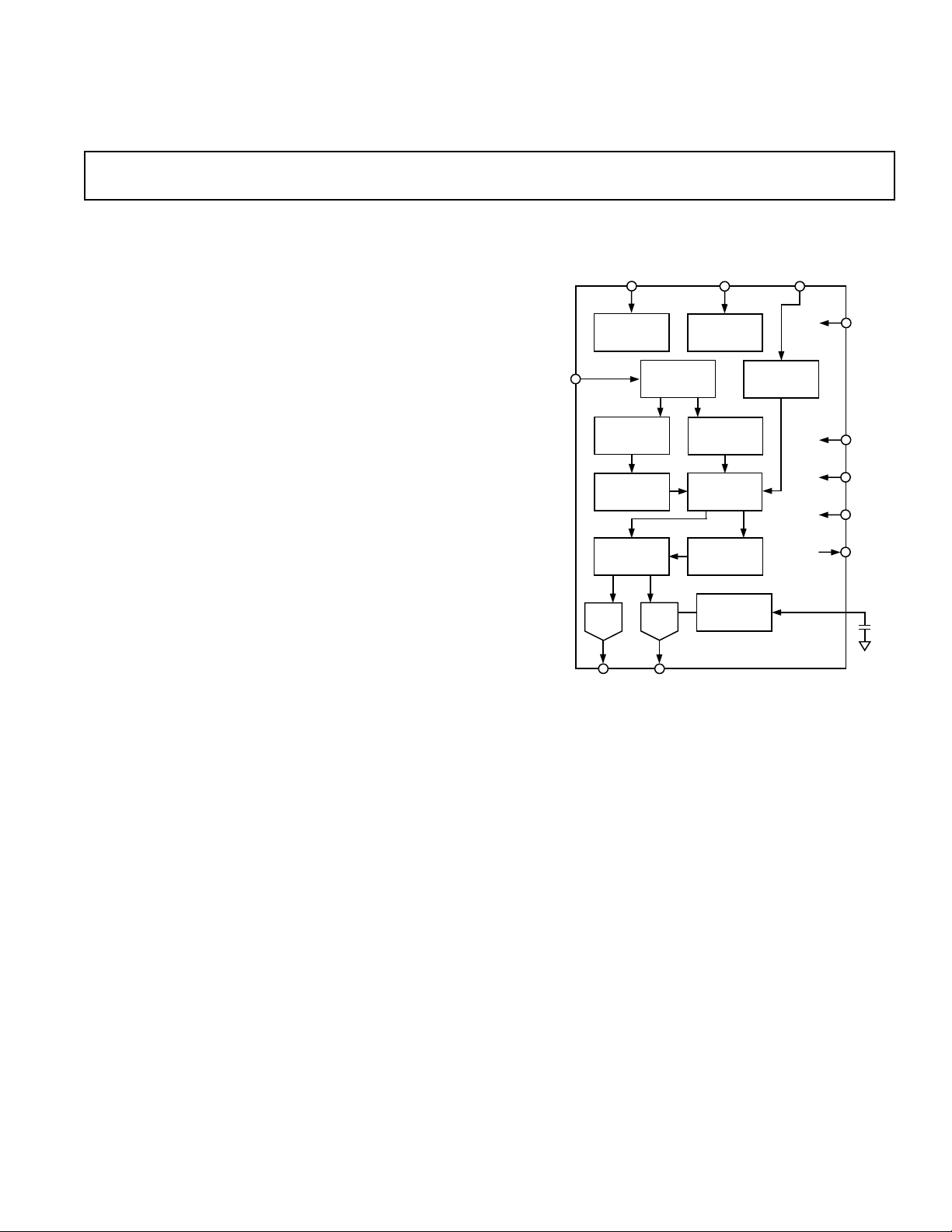
AD1955
FUNCTIONAL BLOCK DIAGRAM
DSD
BITSTREAM
INPUT
4
DIGITAL
SUPPLY
DSD FILTER
RESET
MUTE
ANALOG
SUPPLY
ZERO
FLAGS
(continued on page 12)
16-/20-/24-BIT
AUDIO DATA/
EXTERNAL
DIGITAL
FILTER INPUT
MASTER
CLOCK INPUT
AUTO -CLOCK
DIVIDER
3/4
SERIAL DATA
INTERFACE
DIGITAL
FILTER ENGINE
NOISE-SHAPED
SCRAMBLING
I-DAC
L-CH R-CH
DIFFERENTIAL
CURRENT OUTPUT
I-DAC
MUX
CONTROL
DATA INPUT
3
SPI CONTROL
EXTERNAL
FILTER I/F
S/H
MULTIBIT -
MODULATOR
VOLTA G E
REFERENCE
PRODUCT OVERVIEW
The AD1955 is a complete, high performance, single-chip, stereo
digital audio playback system. It is comprised of a multibit sigmadelta modulator, high performance digital interpolation filters,
and continuous-time differential current output DACs. Other
features include an on-chip clickless stereo attenuator and mute
capability, programmed through an SPI compatible serial control
port. The AD1955 is fully compatible with all known DVD audio
formats including 192 kHz as well as 96 kHz sample frequencies
and 24 bits. It is also backward compatible by supporting 50 µs/
15 µs digital de-emphasis intended for “redbook” compact discs,
as well as de-emphasis at 32 kHz and 48 kHz sample rates.
The AD1955 has a very flexible serial data input port that
allows for glueless interconnection to a variety of ADCs, DSPs,
SACD decoders, external digital filters, AES/EBU receivers, and
REV. 0
Information furnished by Analog Devices is believed to be accurate and
reliable. However, no responsibility is assumed by Analog Devices for its
use, nor for any infringements of patents or other rights of third parties that
may result from its use. No license is granted by implication or otherwise
under any patent or patent rights of Analog Devices.
One Technology Way, P.O. Box 9106, Norwood, MA 02062-9106, U.S.A.
Tel: 781/329-4700 www.analog.com
Fax: 781/326-8703 © Analog Devices, Inc., 2002
Page 2

AD1955–SPECIFICATIONS
TEST CONDITIONS
(Unless otherwise noted.)
Analog Supply Voltages (AVDD) . . . . . . . . . . . . . . . . . . . . 5 V
Digital Supply Voltages (DV
Reference Current (I
Ambient Temperature . . . . . . . . . . . . . . . . . . . . . . . . . . . 25°C
Input Clock . . . . . . . . . . . . . . . . . . . . . . . . . . . . . 12.288 MHz
Input Signal . . . . . . . . . . . . . . . . . 984.375 Hz, 0 dB Full Scale
Input Sample Rate . . . . . . . . . . . . . . . . . . . . . . . . . . . . 48 kHz
Measurement Bandwidth . . . . . . . . . . . . . . . . 20 Hz to 20 kHz
Word Width . . . . . . . . . . . . . . . . . . . . . . . . . . . . . . . . . 24 Bits
Load Capacitance . . . . . . . . . . . . . . . . . . . . . . . . . . . . 100 pF
Load Impedance . . . . . . . . . . . . . . . . . . . . . . . . . . . . . . 47 kΩ
Input Voltage HI . . . . . . . . . . . . . . . . . . . . . . . . . . . . . . . 2.4 V
Input Voltage LO . . . . . . . . . . . . . . . . . . . . . . . . . . . . . . 0.8 V
REF
) . . . . . . . . . . . . . . . . . . . . 5 V
DD
) . . . . . . . . . . . . . . . . . . . . . 0.960 mA
ANALOG PERFORMANCE
Parameter Min Typ Max Unit
Resolution 24 Bits
SIGNAL-TO-NOISE RATIO (20 Hz to 20 kHz)*
Differential Output (A-Weighted, RMS) (Stereo) 120 114 dB
Differential Output (A-Weighted, RMS) (Mono) 123 dB
Single-Ended (A-Weighted, RMS) (Stereo) 119 dB
DYNAMIC RANGE (20 Hz to 20 kHz, –60 dB Input)*
Differential Output (A-Weighted, RMS) (Stereo) 120 114 dB
Differential Output (A-Weighted, RMS) (Mono) 123 dB
Single-Ended (A-Weighted, RMS) (Stereo) 119 dB
Total Harmonic Distortion + Noise (Stereo) at 0 dBFS –110 –102.5 dB
ANALOG OUTPUTS
Differential Output Range (Full Scale) 8.64 mA p-p
Output Capacitance at Each Output Pin 100 pF
Output Bias Current, Each Output –3.24 mA
Out-of-Band Energy (0.5 f
Reference Voltage 2.245 2.39 2.505 V
DC ACCURACY
Gain Error ± 6%
Interchannel Gain Mismatch 0.01 0.26 dB
Gain Drift 25 ppm/°C
Interchannel Crosstalk (EIAJ Method) –125 dB
Interchannel Phase Deviation ± 0.1 Degrees
Mute Attenuation –100 dB
De-Emphasis Gain Error ± 0.1 dB
*Measured with Audio Precision System Two Cascade in RMS Mode. Averaging Mode will show approximately 2 dB better performance.
Performance of right and left channels are identical (exclusive of the Interchannel Gain Mismatch and Interchannel Phase Deviation specifications).
Specifications subject to change without notice.
to 100 kHz) –90 dB
S
(See figures. I
= 0.960 mA, V
REF
= 2.80 V.)
BIAS
REV. 0–2–
Page 3

AD1955
DIGITAL I/O
Parameter Min Typ Max Unit
Input Voltage HI (V
Input Voltage LO (V
Input Leakage (I
Input Leakage (I
High Level Output Voltage (V
Low Level Output Voltage (V
Input Capacitance 20 pF
Specifications subject to change without notice.
(–40C to +85C, unless otherwise noted.)
) 2.2 V
IH
) 0.8 V
IL
@ VIH = 2.4 V) –3+3µA
IH
@ VIL = 0.8 V) –3+3µA
IL
) IOH = 1 mA 2.4 V
OH
) IOL = 1 mA 0.4 V
OL
TEMPERATURE
Parameter Min Typ Max Unit
Specifications Guaranteed 25 °C
Functionality Guaranteed –40 +85 °C
Storage –55 +125 °C
Specifications subject to change without notice.
POWER
Parameter Min Typ Max Unit
SUPPLIES
Voltage, Digital 4.50 5 5.50 V
Voltage, Analog 4.50 5 5.50 V
Analog Current 20 mA
Analog Current—Reset 20 mA
Digital Current 22 mA
Digital Current—Reset 2 mA
DISSIPATION
Operation—Both Supplies 210 mW
Operation—Analog Supply 100 mW
Operation—Digital Supply 110 mW
POWER SUPPLY REJECTION RATIO
1 kHz 300 mV p-p Signal at Analog Supply Pins –77 dB
20 kHz 300 mV p-p Signal at Analog Supply Pins –72 dB
Specifications subject to change without notice.
DIGITAL FILTER CHARACTERISTICS
Stop-Band
Sample Rate (kHz) Pass Band (kHz) Stop Band (kHz) Attenuation (dB) Pass-Band Ripple (dB)
44.1 DC–20 24.1–328.7 110 ± 0.0002
48 DC–21.8 26.23–358.28 110 ±0.0002
96 DC–39.95 56.9–327.65 115 ±0.0005
192 DC–87.2 117–327.65 95 0/–0.04 (DC – 21.8 kHz)
0/–0.5 (DC – 65.4 kHz)
0/–1.5 (DC – 87.2 kHz)
Specifications subject to change without notice.
REV. 0
–3–
Page 4

AD1955
SPECIFICATIONS
(continued)
GROUP DELAY
Chip Mode Group Delay Calculation fS (kHz) Group Delay Unit
INT8 Mode 5553/(128 f
INT4 Mode 5601/(64 f
INT2 Mode 5659/(32 fS) 192 921 µs
Specifications subject to change without notice.
DIGITAL TIMING
(Guaranteed over –40C to +85C, AVDD = DVDD = 5.0 V 10%.)
Parameter Description Min Unit
t
DMP
t
DML
t
DMH
t
DBH
t
DBL
t
DBP
t
DLS
t
DLH
t
DWH
t
DWL
t
DDS
t
DDH
t
DPHS
t
DSDS
t
DSDH
t
DSKP
t
DSKH
t
DSKL
t
DMP
t
DML
t
DMH
t
CLS
t
CLH
t
CDS
t
CDH
t
RSTL
Specifications subject to change without notice.
MCLK Period (F
MCLK LO Pulsewidth (All Modes) 0.4 t
MCLK HI Pulsewidth (All Modes) 0.4 t
BCLK/EF_BCLK High 20 ns
BCLK/EF_BCLK Low 20 ns
BCLK/EF_BCLK Period 60 ns
LRCLK/EF_WCLK Setup 0 ns
LRCLK Hold (DSP Serial Port Mode Only) 15 ns
EF_WCLK High 20 ns
EF_WCLK Low 20 ns
SDATA/EF_LDATA/EF_RDATA Setup 0 ns
SDATA/EF_LDATA/EF_RDATA Hold 20 ns
DSD_PHASE Setup 20 ns
DSD_DATA Setup 5 ns
DSD_DATA Hold 5 ns
DSD_SCLK Period 60 ns
DSD_SCLK High 20 ns
DSD_SCLK Low 20 ns
CCLK Period 50 ns
CCLK LO Pulsewidth 15 ns
CCLK HI Pulsewidth 10 ns
CLATCH Setup 0 ns
CLATCH Hold 15 ns
CDATA Setup 0 ns
CDATA Hold 5 ns
RST LO Pulsewidth 10 ns
)48903.8 µs
S
)96911.6 µs
S
MCLK
= 256 F
)50ns
LRCLK
DMP
DMP
ns
ns
REV. 0–4–
Page 5
AD1955
H
ABSOLUTE MAXIMUM RATINGS
*
Parameter Min Max Unit
to DGND –0.3 6 V
DV
DD
AV
to AGND –0.3 6 V
DD
Digital Inputs DGND – 0.3 DV
Analog Outputs AGND – 0.3 AV
+ 0.3 V
DD
+ 0.3 V
DD
AGND to DGND –0.3 +0.3 V
Reference Voltage (AV
+ 0.3)/2
DD
Soldering 300 °C
10 sec
*Stresses greater than those listed under Absolute Maximum Ratings may cause
permanent damage to the device. This is a stress rating only; functional operation
of the device at these or any other conditions above those indicated in the
operational section of this specification is not implied. Exposure to absolute
maximum rating conditions for extended periods may affect device reliability.
ORDERING GUIDE
Model Temperature Package Description Package Option
AD1955ARS –40°C to +85°C 28-Lead SSOP RS-28
AD1955ARSRL –40°C to +85°C 28-Lead SSOP RS-28 on 13" Reels
EVAL-AD1955EB Evaluation Board
*RS = Shrink Small Outline Package
PACKAGE CHARACTERISTICS
Package Typ Unit
(Thermal Resistance 109.0 °C/W
JA
[Junction-to-Ambient])
(Thermal Resistance 39.0 °C/W
JC
[Junction-to-Case])
*
PIN CONFIGURATION
DVDD
LRCLK/EF_WCLK
BCLK/EF_BCLK
SDATA/EF_LDATA
EF_RDATA
DSD_SCLK
DSD_LDATA
DSD_RDATA
DSD_PHASE
AGND
IOUTR+
IOUTR–
FILTR
IREF
1
2
3
4
5
6
AD1955
7
TOP VIEW
(Not to Scale)
8
9
10
11
12
13
14
28
27
26
25
24
23
22
21
20
19
18
17
16
15
DGND
MCLK
CCLK
CLATC
CDATA
PD/RST
MUTE
ZEROL
ZEROR
AGND
IOUTL+
IOUTL–
FILTB
AVDD
CAUTION
ESD (electrostatic discharge) sensitive device. Electrostatic charges as high as 4000 V readily
accumulate on the human body and test equipment and can discharge without detection. Although the
AD1955 features proprietary ESD protection circuitry, permanent damage may occur on devices
subjected to high energy electrostatic discharges. Therefore, proper ESD precautions are recommended
to avoid performance degradation or loss of functionality.
WARNING!
ESD SENSITIVE DEVICE
REV. 0
–5–
Page 6

AD1955
PIN FUNCTION DESCRIPTIONS
Pin No. I/O Mnemonic Description
1 DVDD Digital Power Supply Connected to Digital 5 V Supply
2 Input LRCLK/EF_WCLK Left/Right Clock Input for Input Data in PCM Mode
Word Clock in External Filter Mode
3 Input BCLK/EF_BCLK Bit Clock Input for Input Data in PCM Mode
Bit Clock Input in External Filter Mode
4 Input SDATA/EF_LDATA MSB First, Twos Complement Serial Audio Data
Two Channel (left and right), 16-Bit to 24-Bit Data in PCM Mode
Left Channel Data in External Filter Mode
5 Input EF_RDATA Not used in PCM Mode
Right channel data in External Filter Mode
6 I/O DSD_SCLK
7 Input DSD_LDATA DSD Left Channel Data Input
8 Input DSD_RDATA DSD Right Channel Data Input
9 I/O DSD_PHASE DSD Phase Reference Signal. This clock should be 64 44.1 kHz,
10 AGND Analog Ground
11 Output IOUTR+ Right Channel Positive Analog Output
12 Output IOUTR– Right Channel Negative Analog Output
13 Output FILTR Voltage Reference Filter Capacitor Connection. Bypass and decouple the
14 IREF Connection Point for External Bias Resistor
15 AVDD Analog Power Supply Connected to Analog 5 V Supply
16 Output FILTB Filter Capacitor Connection with Parallel 10 µF and 0.1 µF Capacitors to AGND
17 Output IOUTL– Left Channel Negative Analog Output
18 Output IOUTL+ Left Channel Positive Analog Output
19 AGND Analog Ground
20 Output ZEROR Right Channel Zero Flag Output. This pin goes high when the right channel
21 Output ZEROL Left Channel Zero Flag Output. This pin goes high when the left channel has
22 Input MUTE Mute. Assert high to mute both stereo analog outputs. Deassert low for nor-
23 Input PD/RST Power Down/Reset. The AD1955 is placed in a reset state and the digital
24 Input CDATA Serial Control Input, MSB First, Containing 16 Bits of Unsigned Data. Used
25 Input CLATCH Latch Input for Control Data
26 Input CCLK Clock Input for Control Data. Control input data must be valid on the rising
27 Input MCLK Master Clock Input. Connect to an external clock source.
28 DGND Digital Ground
Serial Clock Input for DSD Data. This clock should be 64 44.1 kHz,
2.8224 MHz or 128 44.1 kHz, 5.6448 MHz in Normal Mode, 128
44.1 kHz, 5.6448 MHz or 256 44.1 kHz, 11.2896 MHz in Phase Mode.
2.8224 MHz. If not used, this pin should be connected low.
voltage reference with parallel 10 µF and 0.1 µF capacitors to AGND.
has no signal input or the DSD mute pattern is detected.
no signal input or the DSD mute pattern is detected.
mal operation.
circuitry is powered down when this pin is held low. The AD1955 is reset on
the rising edge of this signal. The serial control port registers are reset to the
default values. Connect high for normal operation.
for specifying control information and channel-specific attenuation.
edge of CCLK. CCLK may be continuous or gated.
REV. 0–6–
Page 7
Typical Performance Characteristics–AD1955
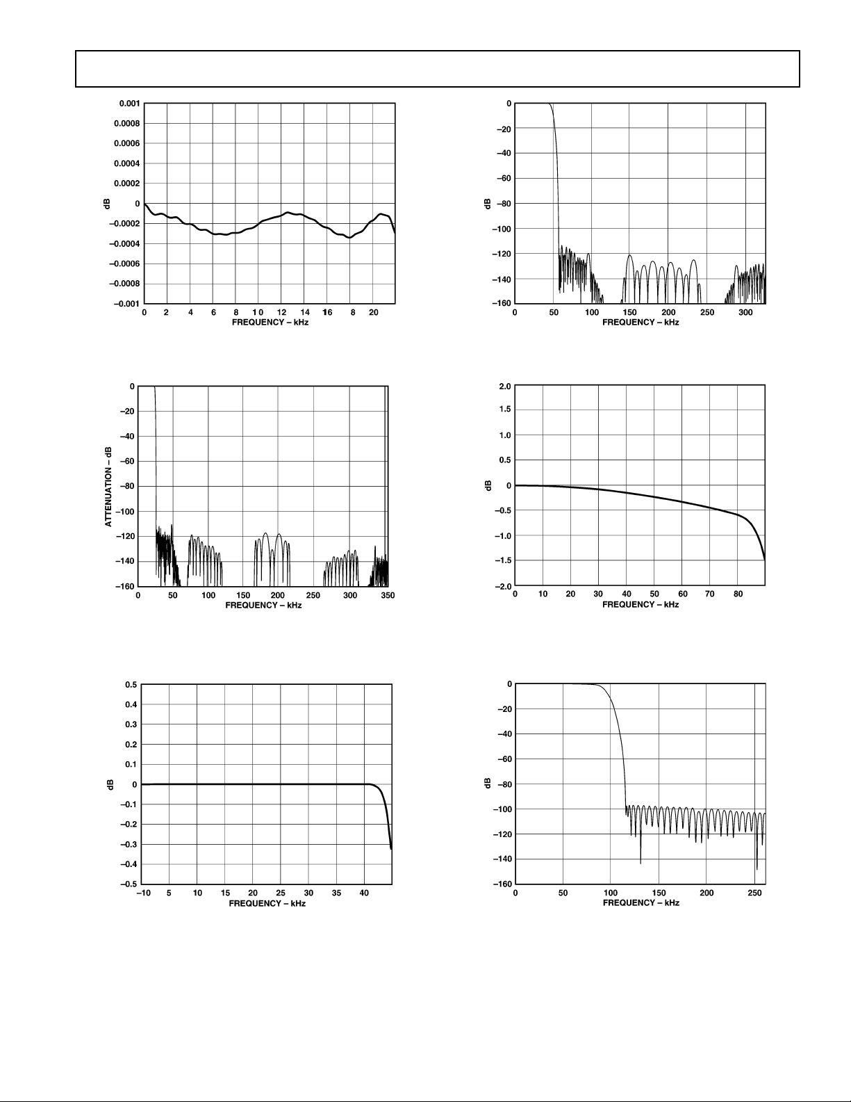
TPC 1. Pass-Band Response, 8 Mode, 48 kHz Sample Rate
TPC 2. Complete Response, 8 Mode, 48 kHz Sample Rate
TPC 4. Complete Response, 4 Mode, 96 kHz Sample Rate
TPC 5. Pass-Band Response, 2 Mode, 192 kHz
Sample Rate
TPC 3. 44 kHz Pass-Band Response 4 Mode, 96 kHz
Sample Rate
REV. 0
–7–
TPC 6
. Complete Response, 2 Mode, 192 kHz
Sample Rate
Page 8
AD1955
TPC 7. DSD Digital Filter Pass Band
TPC 8. DSD Digital Filter Response, Input Sample
Rate = 2.8224 MHz
TPC 10. FFT Plot, DNR = 121 dBFS (A-Weight), PCM
SR = 48 kHz, –60 dBFS @ 1 kHz
TPC 11. FFT Plot, SNR = 121 dBFS (A-Weight), PCM
SR = 48 kHz with Zero Input
TPC 9. FFT Plot, THD + N = –110 dBFS, PCM SR = 48
kHz,
0 dBFS @ 1 kHz
TPC 12. Linearity, PCM SR = 48 kHz, 0 dBFS to
–140 dBFS Input @ 200 Hz
REV. 0–8–
Page 9

AD1955
TPC 13. THD + N vs. Amplitude Plot, PCM SR = 48
0 dBFS to –120 dBFS Input @ 1 kHz
kHz,
TPC 14. THD + N vs. Frequency Plot, PCM SR = 48
kHz,
0 dBFS Input
TPC 16. Wideband FFT Plot, PCM SR = 48 kHz, 0
dBFS @ 20 kHz
TPC 17. De-emphasis Frequency Response, PCM SR =
32 kHz,
0 dBFS Input
TPC 15. FFT Plot, PCM SR = 48 kHz, 0 dBFS @ 20
kHz, BW = 22 kHz
REV. 0
TPC 18.
SR = 44.1 kHz, 0 dBFS Input
–9–
De-emphasis
Frequency Response, PCM
Page 10

AD1955
TPC 19.
SR = 48 kHz, 0 dBFS Input
TPC 20. FFT Plot, PCM SR = 96 kHz, 0 dBFS @ 1 kHz,
BW = 22 kHz
De-emphasis
Frequency Response, PCM
TPC 22. FFT Plot, PCM SR = 96 kHz, Zero Input,
BW = 22 kHz
TPC 23. Wideband FFT Plot, PCM SR = 96 kHz,
0 dBFS Input @ 37 kHz
TPC 21. FFT Plot, PCM SR = 96 kHz, –60 dBFS @
1 kHz, BW = 22 kHz
TPC 24. FFT Plot, PCM SR = 192 kHz, 0 dBFS Input
@ 1 kHz
REV. 0–10–
Page 11

AD1955
TPC 25. FFT Plot, PCM SR = 192 kHz, –60 dBFS Input
@ 1 kHz
TPC 26. FFT Plot, PCM SR = 192 kHz, Zero Input
TPC 28. FFT Plot, 64 fS DSD, SR = 44.1 kHz,
0 dBFS @ 1 kHz
TPC 29. FFT Plot, 64 fS DSD, SR = 44.1 kHz,
–60 dBFS @ 1 kHz
TPC 27. Wideband FFT Plot, PCM SR = 192 kHz,
0 dBFS @ 60 kHz
REV. 0
TPC 30. FFT Plot, 64 fS DSD, SR = 44.1 kHz, Zero Input
–11–
Page 12

AD1955
TPC 31. FFT Plot, 64 fS DSD, SR = 44.1 kHz,
0 dBFS @ 10 kHz
(continued from page 1)
sample rate converters. The AD1955 can be configured in leftjustified, I
2
S, right-justified, or DSP serial port compatible
modes. It can support MSB first, twos complement format, 16,
18, 20, and 24 bits in all standard PCM modes. The AD1955
also has an interface for SACD playback and an external digital
filter interface for use with an external digital interpolation filter
or HDCD decoder. The AD1955 uses a 5 V power supply. It is
fabricated on a single monolithic integrated circuit and is housed
in a 28-lead SSOP package for operation over the temperature
range –40°C to +85°C.
OPERATING FEATURES
Serial Data Input Port
The AD1955’s flexible serial data input port accepts standard
PCM audio data and external digital filter output data in twos
complement, MSB-first format in PCM/External Digital Filter
Mode, and a dedicated SACD serial port accepts DSD bit stream
data in SACD Mode. If the PCM Mode is selected by Control
Register 0 Bits 12 and 13, the left channel data field always precedes the right channel data field. The serial data format and
word length in PCM Mode are set by the mode select bits (Bits 4
and 5 and Bits 2 and 3, respectively) in the SPI control register.
In all data formats except for the Right-Justified Mode, the
serial port will accept an arbitrary number of bits up to a limit of
24 (extra bits will not cause an error, but they will be truncated
internally). In Right-Justified Mode, Control Register 0, Bits 2
and 3 are used to set the word length to 16, 18, 20, or 24 bits.
The default on power up is 24-bit, I
2
S.
In the External Digital Filter Mode, selected by Control Register 0 Bits 12 and 13, Bits 2 and 3 are used to set the word length
to 16, 18, 20, or 24 bits and the format is set with Bits 4 and 5.
For a burst-mode clock, the format should be set to left-justified.
DSP Mode is not used. The LRCLK is always falling-edge active.
The default on power-up is 24-bit mode in PCM and External
Digital Filter Mode.
In SACD Mode, selected by Control Register 0 Bits 12 and 13,
the SACD port will accept a DSD bit stream.
When the SPI Control Port is not being used, the SPI pins (24,
25, and 26) should be tied to DGND or DVDD.
TPC 32. Wideband FFT Plot, 64 fS DSD,
SR = 44.1 kHz, 0 dBFS @ 10 kHz
Serial Data Format in PCM Mode
The supported formats are shown in Figure 1. For detailed
timing, see Figure 2.
In Left-Justified Mode, LRCLK is high for the left channel and
low for the right channel. Data should be valid on the rising
edge of BCLK. The MSB is left-justified to an LRCLK transition, with no MSB delay.
2
In I
S Mode, LRCLK is low for the left channel and high for
the right channel. Data should be valid on the rising edge of
BCLK. The MSB is left-justified to an LRCLK transition but
with a single BCLK period delay.
In DSP serial port mode, LRCLK must pulse high for at least
one bit clock period before the MSB of the left channel is valid,
and LRCLK must pulse high again for at least one bit clock
period before the MSB of the right channel is valid. Data should
be valid on the falling edge of BCLK. The DSP serial port mode
can be used with any word length up to 24 bits.
In this mode, it is the responsibility of the DSP to ensure that the
left data is transmitted with the first LRCLK pulse after RESET,
and that synchronism is maintained from that point forward.
In Right-Justified Mode (16 bits shown), LRCLK is high for the
left channel and low for the right channel. Data should be valid
on the rising edge of BCLK.
In normal operation, there are 64 bit clocks per frame (or 32 per
half-frame). When the SPI word length control bits (Bits 2 and
3 in Control Register 0) are set to 24 bits (0:0), the serial port
will begin to accept data starting at the eighth bit clock pulse
after the LRCLK transition. When the word length control bits
are set to 20-bit mode, data is accepted starting at the 12
clock position. In 18-bit mode, data is accepted starting at the
th
bit clock position. In 16-bit mode, data is accepted starting
14
th
bit
at the 16th bit clock position.
Note that the AD1955 is capable of a 32 f
BCLK frequency
S
“packed mode” where the MSB is left-justified to an LRCLK
transition, and the LSB is right-justified to the next LRCLK
transition. LRCLK is high for the left channel, and low for the
right channel. Data is valid on the rising edge of BCLK. Packed
mode can be used when the AD1955 is programmed in LeftJustified Mode.
REV. 0–12–
Page 13

AD1955
Serial Data Format in External Digital Filter Mode
In the External Digital Filter Mode, the AD1955 will accept
up to 24-bit serial, twos complement, MSB-first data from an
external digital filter, an HDCD decoder, or a general-purpose
DSP. If the External Digital Filter Mode is selected by Control
Register 0, Bits 12 and 13, Pin 2 to Pin 5 are assigned as the word
clock input (EF_WCLK, Pin 2), bit clock input (EF_BCLK,
Pin 3), left channel data input (EF_LDATA, Pin 4), and right
channel data input (EF_RDATA, Pin 5), respectively, to accept
(48 kHz), 4fS (96 kHz), or 2fS (196 kHz) oversampled data.
8f
S
Left and right channel data should be valid on the rising edge
of EF_BCLK. The mode can be set to Left- or Right-Justified.
A burst mode BCLK can be used in Left-Justified Mode.
Serial Data Format in SACD Mode
In the SACD Mode, the AD1955 supports both normal mode
or phase modulation mode, which are selected by Control
Register 1, Bit 6. If normal mode is selected, DSD_SCLK,
DSD_LDATA, and DSD_RDATA are used to interface with
DSD decoder chip. In this mode, the DSD data is clocked in
the AD1955 using the rising edge of DSD_SCLK with a 64f
S
rate, 2.8224 MHz. DSD_PHASE pin should be connected LOW.
If Phase Modulation Mode is selected, the DSD_PHASE pin is
also used to interface with the DSD decoder. In this mode, a
DSD_PHASE signal is used as a reference signal to receive
64f
S
data from the decoder. The DSD data is clocked into the
the
AD1955 with a 128fS DSD_SCLK.
The AD1955 can operate as a master or slave device. In Master
Mode, the AD1955 will output DSD_SCLK and DSD_PHASE
(if in Phase Modulation Mode) to a DSD decoder and will
support Normal Mode and Phase Modulation Mode 0. In Slave
Mode, the AD1955 will accept DSD_SCLK and DSD_PHASE
(if in Phase Modulation Mode) from a DSD decoder and supports all of the normal and phase modulation modes.
When the SACD Port is not being used, the SACD pins (Pins
6, 7, 8, and 9) should be tied to a valid logic level. Please note
that there are weak pull-ups (0.6 mA typical) on DSD_SCLK
and DSD_PHASE.
Master Clock
The AD1955 must be set to the proper sample rate and master
clock rate using Control Registers 0 and 1. The allowable master
clock frequencies for each interpolation mode are shown below.
In the External Filter Mode, the AD1955 accepts master clock
frequencies depending on the input sample rate as shown below.
In the SACD Mode, the AD1955 accepts a 256fS, 512fS, or
Master Clock, where fS is nominally 44.1 kHz. In Slave
768f
S
Mode, by default, the rising edge of DSD_SCLK should coincide
with the rising edge of MCLK. Control Register 1, Bit 2 should
be set to 1 if the rising edge of DSD_SCLK coincides with the
falling edge
of MCLK. In Master Mode this bit can be used to
select the MCLK edge used to generate the DSD clock outputs.
Zero Detection
When the AD1955 detects that the audio input data is continu-
ously zero during 1024 LRCLK periods in PCM Mode or 8192
LRCLK periods in 8f
External Digital Filter Mode, ZEROL
S
(Pin 21) or ZEROR (Pin 20) is set to active.
When the AD1955 is in SACD Mode, it will detect an SACD
mute pattern. If the input bit stream shows a mute pattern for
about 22 ms, the AD1955 will set ZEROL (Pin 21) or ZEROR
(Pin 20) to active. The outputs can be set to active high or low
using Control Register 1, Bit 8.
Reset/Power-Down
The AD1955 will be reset when the PD/RST pin is set low. The
part may be powered down using Bit 15, Control Register 0.
Audio Outputs
Active I/V con
outputs at
verters should be used, which will hold the DAC
a constant voltage level. Passive I/V conversion should
not be used, since the DAC performance will be seriously degraded.
For best THD + N performance over temperature, a reference
voltage of 2.80 V should be used with the I/V converters. For a
lower parts count, the voltage at FILTR can be used. In this
instance, THD + N performance at high temperature can be
improved by reducing I
, with an attendant reduction in gain
REF
(linear dependence) and DNR/SNR (square-root dependence).
The AD1955 audio outputs sink a current proportional to the
input signal, superimposed on a steady bias current. The current-to-voltage (I/V) converters used need to be able to supply
this bias current, as well as the signal current, or a resistor or
current source can be used to a positive voltage to null this
current in order to center the range of the I/V converters.
If pull-up resistors are used to bring the output of the I/V converters to 0 V for maximum headroom and THD balance, as shown
in the applications circuits, the following equation can be used:
RVVIVR
=
PULLUP SUPPLY BIAS BIAS BIAS I V
[]
– ()
+
[]
/
Interpolation Mode
48 kHz (INT 8×) Mode
96 kHz (INT 4×) Mode
192 kHz (INT 2×) Mode
Input Sample Rate
8 × f
S
4 × f
S
2 × f
S
REV. 0
PCM Mode
Allowable Master Clock Frequencies (ⴛ fS)Nominal Input
64 96 128 192 256 384 512 768
•••
•••
•••
External Filter Mode
Allowable Master Clock Frequencies (ⴛ fS)Nominal Input Sample Rate
64 96 128 192 256 384 512 768
•••
•••
•••
–13–
Sample Rate (kHz)
32, 44.1, 48
88.2, 96
176.4, 192
(to External Filter) (kHz)
32, 44.1, 48
88.2, 96
176.4, 192
Page 14

AD1955
For example, with the stereo circuits given in Figures 7 through
10, this gives:
12 0 2 80 3 24 2 80 2 00 1 98. – .. .. .VV mA VK k
[]
[]
+
()
=Ω
A 2.00 kΩ resistor is used.
The supply used should be as quiet as possible.
SPI REGISTER DEFINITIONS
Table I. DAC Control Register 0
Bit Description Value Definition
15 Power-Down 0 Operation
1Powered Down
14 Mute 0 Not Muted
1 Muted
13:12 Data Format 00 PCM
01 External DF
10 SACD Slave
11 SACD Master
11:10 Output Format 00 Stereo
01 Not Allowed
10 Mono Left
11 Mono Right
9:8 PCM Sample Rate 00 48 kHz
01 96 kHz
10 192 kHz
11 Reserved
7:6 De-Emphasis Curve 00 None
Select 01 44.1 kHz
10 32 kHz
11 48 kHz
2
5:4 PCM/EF Serial Data 00 I
S
Format 01 Right-Justified
10 DSP
11 Left-Justified
3:2 PCM/EF Serial Data 00 24 bits
Width 01 20 bits
10 18 bits
11 16 bits
1:0 SPI Register Address 00
Default = 0
Serial Control Port
The AD1955 has an SPI compatible control port to permit programming the internal control registers. The SPI control port is
a 3-wire serial port. Its format is similar to the Motorola SPI
format except that the input data-word is 16 bits wide. The serial
bit clock may be completely asynchronous to the sample rate of the
DAC. The following figure shows the format of the SPI signal
Note that the CCLK may be continuous or a 16-clock burst.
Table II. DAC Control Register 1
Bit Description Value Definition
10:9 MCLK Mode 00 256 f
01 512 f
10 768 f
S
S
S
11 Reserved
8Zero Flag Polarity 0 Active High
1Active Low
7SACD Bit Rate 0 64 f
1 128 f
S
S
6SACD Mode 0 Normal
1 Phase Mode
5:4 SACD Phase Select 00 Phase 0
01 Phase 1
10 Phase 2
11 Phase 3
3SACD Bit Inversion 0 Normal
1 Inverted
2SACD MCLK to 0 Rising Edge
BCLK Phase 1 Falling Edge
1:0 SPI Register Address 01
Default = 0
Table III. DAC Volume Registers
Bit Description Value Definition
14-Bit
15:2 Volume Unsigned
1:0 SPI Register Address 10 Left Volume
11 Right Volume
Default = Full Volume
REV. 0–14–
Page 15

AD1955
LRCLK
BCLK
SDATA
LRCLK
BCLK
SDATA
LRCLK
BCLK
SDATA
LRCLK
BCLK
SDATA
MSB
NOTES
1. DSP MODE DOES NOT IDENTIFY CHANNEL.
2. LRCLK NORMALLY OPERATES AT
3. BCLK FREQUENCY IS NORMALLY 64 LRCLK BUT MAY BE OPERATED IN BURST MODE.
MSB
MSB
LEFT CHANNEL
I
LEFT CHANNEL
MSB
RIGHT-JUSTIFIED MODE – SELECT NUMBER OF BITS PER CHANNEL
DSP MODE – 16 TO 24 BITS PER CHANNEL
LEFT CHANNEL
LSB
LEFT-JUSTIFIED MODE – 16 TO 24 BITS PER CHANNEL
f
EXCEPT FOR DSP MODE, WHICH IS 2 fS.
S
LSB
2
S MODE –16 TO 24 BITS PER CHANNEL
LSB
Figure 1. Supported Serial Data Formats
RIGHT CHANNEL
MSB
RIGHT CHANNEL
MSB
MSB
RIGHT CHANNEL
MSB
1/f
S
LSB
LSB
LSB
LSB
BCLK
L/RCLK
SDATA
LEFT-JUSTIFIED
RIGH T-JUSTIFIED
MODE
SDATA
2
I
S-JUSTIFIED
MODE
SDATA
MODE
t
DBH
t
DBL
t
DLS
t
DDS
MSB
t
DDH
8-BIT CLOCKS
(24-BIT DATA)
12-BIT CLOCKS
(20-BIT DATA)
16-BIT CLOCKS
(16-BIT DATA)
t
DBP
MSB-1
t
DDS
MSB
t
DDH
Figure 2. Serial Data Port Timing
t
DDS
MSB
t
DDH
t
DDS
LSB
t
DDH
REV. 0
–15–
Page 16

AD1955
NORMAL
MODE
PHASE
MOD
MODE
DSD_PHASE_0
DSD_PHASE_1
DSD_PHASE_2
DSD_PHASE_3
DSD_LDATA, DSD_RDATA
DSD_DATA
DSD_BCLK
DSD_DATA
DSD_BCLK
DSD_PHASE
DSD_SCLK
D0 D1
D0
D0
Figure 3. DSD Modes
t
DPHS
t
DSDS
t
DSDH
t
DSKH
t
DSKP
t
DSKL
CLATCH
CCLK
CDATA
Figure 4. DSD Serial Port Timing
t
CLATCHH
t
t
CLKH
D15 D14 D0
t
t
CDS
CDH
CLKL
Figure 5. Serial Control Port Timing
REV. 0–16–
Page 17

AD1955
MCLK
RDATA
SDATA
BCLK
LRCLK
DSD_PHASE
DSD_RDATA
DSD_LDATA
DSD_SCLK
CDATA
CLATCH
CCLK
MUTE
ZEROR
ZEROL
PD/RST
DVD D
C1
0.1F
DVD D AV DD
MCLK
EF_RDATA
SDATA/EF_LDATA
BCLK/EF_BCLK
LRCLK/EF_WCLK
DSD_PHASE
DSD_RDATA
DSD_LDATA
DSD_SCLK
CDATA
CLATCH
CCLK
MUTE
ZEROR
ZEROL
PD/RST
DGND
L2
600Z
AD1955
U1
AGND1
AV DD
L3
600Z
AGND2
0.1F
IOUTL+
IOUTL–
IOUTR+
IOUTR–
FILTR
FILTB
IREF
CONNECT VBIAS TO VREFA FOR BEST PERFORMANCE
OR VREF FOR LOWER PARTS COUNT
C2
AV DD
VREF
VBIAS
OR
VREFA
C44
0.1F
VREFA
2.80V
IOUTL+
IOUTL–
IOUTR+
IOUTR–
R56
2.21k⍀
+
R57
2.80k⍀
C5
0.1F
+
C4
10F
C43
47F
VREF
2.39V
+
C6
47F
600Z
L1
R1
2.49k⍀
C3
0.1F
Figure 6. DAC Power Supply and Bypass
REV. 0
–17–
Page 18

AD1955
12V
R6
100
R5
2.00k
C10
100pF
IOUTL+
IOUTL–
VBIAS
C7
OPEN
OPEN
R2
2.00k
C9
C8
100pF
R4
402
R3
2.00k
R7
100
U2-A
AD797
NL+
U3-A
AD797
NL+
2.00k
COMP
NL–
NL–
R8
OUT
COMP
OUT
C11
100pF
AD797
+12V
–12V
R9
1.00k
R10
1.00k
4.7F
4.7F
–3dB at 100 kHz
C13
470pF
R11
1.00k
C12
390pF
R12
1.00k
+
0.1F
+
0.1F
OP AMP BYPASS
DUPLICATE FOR EACH PART
C14
470pF
J1
+
–
G
LEFT
DIRECT
OUT
6VRMS
XLR MALE
Figure 7. Left Channel Differential Output
IOUTR+
IOUTR–
VBIAS
C15
OPEN
C16
OPEN
R13
2.00k
12V
C17
100pF
R15
402
R14
2.00k
R17
100
R18
100
R16
2.00k
U4-A
AD797
NL+
U5-A
AD797
NL+
R19
2.00k
COMP
NL–
NL–
C18
100pF
OUT
COMP
OUT
C19
100pF
AD797
+12V
–12V
R20
1.00k
R21
1.00k
4.7F
4.7F
–3dB at 100 kHz
C21
470pF
R22
1.00k
C20
390pF
R23
1.00k
+
0.1F
+
0.1F
OP AMP BYPASS
DUPLICATE FOR EACH PART
C22
470pF
J2
+
–
G
RIGHT
DIRECT
OUT
6VRMS
XLR MALE
Figure 8. Right Channel Differential Output
REV. 0–18–
Page 19

12V
R28
100
R27
2.00k
C26
100pF
AD1955
IOUTL+
IOUTL–
VBIAS
AD797
C23
OPEN
C24
OPEN
+12V
–12V
R24
2.00k
C25
100pF
R26
402
0.1F
0.1F
OP AMP BYPASS
DUPLICATE FOR EACH PART
R25
2.00k
+
+
4.7F
4.7F
R29
100
U6-A
AD797
NL+
U7-A
AD797
NL+
2.00k
COMP
R30
NL–
NL–
OUT
COMP
OUT
C27
100pF
R31
681
R32
681
R33
226
C28
5.6nF
C29
5.6nF
R36
226
R34
324
R35
324
Figure 9. Left Channel Single-Ended Output
C31
2.7nF
C30
2.7nF
U8-A
AD797
NL+
COMP
NL–
R37
100
OUT
R38
332
–3dB at 75 kHz
C32
3.9nF
R39
OPEN
J3
LEFT
FILTER
OUT
2VRMS
IOUTR+
IOUTR–
VBIAS
AD797
C33
OPEN
C34
OPEN
+12V
R40
2.00k
12V
C35
100pF
R42
402
0.1F
0.1F
R41
2.00k
+
+
4.7F
4.7F
R44
100
R45
100
R43
2.00k
U9-A
AD797
NL+
U10-A
AD797
NL+
R46
2.00k
COMP
NL–
NL–
C36
100pF
OUT
COMP
OUT
C37
100pF
R47
681
R48
681
R49
226
C38
5.6nF
C39
5.6nF
R52
226
R50
324
R51
324
2.7nF
C41
2.7nF
C40
U11-A
AD797
NL+
100
COMP
NL–
R53
OUT
R54
332
–3dB at 75 kHz
C42
3.9nF
R55
OPEN
J4
RIGHT
FILTER
OUT
2VRMS
REV. 0
–12V
OP AMP BYPASS
DUPLICATE FOR EACH PART
Figure 10. Right Channel Single-Ended Output
–19–
Page 20

AD1955
12V
R6
100
R5
1.00k
C10
100pF
IOUTL+
IOUTR–
C7
OPEN
C8
OPEN
IOUTL–
IOUTR+
VBIAS
NOTE REVERSE POLARITY
OF RIGHT CHANNEL OUTPUTS
1.00k
R2
C9
100pF
R4
402
R3
1.00k
U2-A
COMP
AD797
OUT
NL–
R9
1.00k
NL+
U3-A
COMP
R10
1.00k
AD797
OUT
NL–
+12V
NL+
R7
100
R8
1.00k
C11
100pF
AD797
–12V
Figure 11. Mono Differential Output
R11
1.00k
C12
390pF
R12
1.00k
+
0.1F
+
0.1F
OP AMP BYPASS
DUPLICATE FOR EACH PART
–3dB at 100 kHz
C13
470pF
SET CONTROL REGISTER 0, BITS 11:10
TO SELECT LEFT OR RIGHT CHANNEL
4.7F
4.7F
C14
470pF
J1
+
–
G
MONO
DIRECT
OUT
6VRMS
XLR MALE
C23
OPEN
C24
OPEN
1.00k
IOUTL+
IOUTR–
IOUTL–
IOUTR+
VBIAS
NOTE REVERSE
POLARITY OF RIGHT
CHANNEL OUTPUTS
R24
AD797
12V
C25
100pF
R26
402
+12V
R25
1.00k
R28
100
R29
100
0.1F
0.1F
R27
1.00k
U6-A
AD797
NL+
U7-A
AD797
NL+
R30
1.00k
+
+
COMP
NL–
NL–
4.7F
4.7F
C26
100pF
OUT
COMP
OUT
C27
100pF
R31
681
R32
681
R33
226
C28
5.6nF
C29
5.6nF
R36
226
R34
324
R35
324
C30
2.7nF
R37
100
U8-A
COMP
AD797
NL+
C31
2.7nF
SET CONTROL REGISTER 0, BITS 11:10
TO SELECT LEFT OR RIGHT CHANNEL
OUT
NL–
332
R38
3.9nF
–3dB at 75 kHz
C32
R39
OPEN
J3
MONO
FILTER
OUT
2VRMS
–12V
OP AMP BYPASS
DUPLICATE FOR EACH PART
Figure 12. Mono Single-Ended Output
REV. 0–20–
Page 21

OUTLINE DIMENSIONS
Dimensions shown in millimeters
28-Lead Shrink Small Outline Package (SSOP)
(RS-28)
10.50
10.20
9.90
28 15
5.60
8.20
5.30
7.80
5.00
7.40
0.10
COPLANARITY
0.25
0.09
0.05
MIN
1
2.00 MAX
0.65
BSC
14
1.85
1.75
1.65
0.38
0.22
COMPLIANT TO JEDEC STANDARDS MO-150AH
SEATING
PLANE
AD1955
8
4
0
0.95
0.75
0.55
REV. 0
–21–
Page 22

–22–
Page 23

–23–
Page 24

C02805–0–10/02(0)
–24–
PRINTED IN U.S.A.
 Loading...