

Page 1
Four ADCs/Eight DACs with PLL,
A
www.BDTIC.com/ADI
FEATURES
PLL-generated clock or direct master clock
Low EMI design
112 dB DAC/107 dB ADC dynamic range and SNR
−96 dB THD + N
Single 3.3 V supply
Tolerance for 5 V logic inputs
Supports 24-bits and 8 kHz to 192 kHz sample rates
Differential ADC input
Differential DAC output
Log volume control with autoramp function
2
I
C-controllable for flexibility
Software-controllable clickless mute
Software power-down
Right-justified, left-justified, I
Master and slave modes up to 16-channel input/output
Available in a 64-lead LQFP
AECQ-100 qualified
APPLICATIONS
Automotive audio systems
Home theater systems
Set-top boxes
Digital audio effects processors
2
S, and TDM modes
192 kHz, 24-Bit Codec
AD1937
GENERAL DESCRIPTION
The AD1937 is a high performance, single-chip codec that provides
four analog-to-digital converters (ADCs) with differential input
and eight digital-to-analog converters (DACs) with differential
output, using the Analog Devices, Inc., patented multibit sigmadelta (Σ-Δ) architecture. An I
microcontroller to adjust volume and many other parameters.
The AD1937 operates from 3.3 V digital and analog supplies.
The AD1937 is available in a 64-lead (differential output) LQFP.
The AD1937 is designed for low EMI. This consideration is
apparent in both the system and circuit design architectures.
By using the on-board PLL to derive the master clock from the
LR (frame) clock or from an external crystal, the AD1937 eliminates the need for a separate high frequency master clock and
can also be used with a suppressed bit clock. The DACs and
ADCs are designed using the latest Analog Devices continuous
time architecture to further minimize EMI. By using 3.3 V
supplies, power consumption is minimized and further
reduces emissions.
2
C® port is included, allowing a
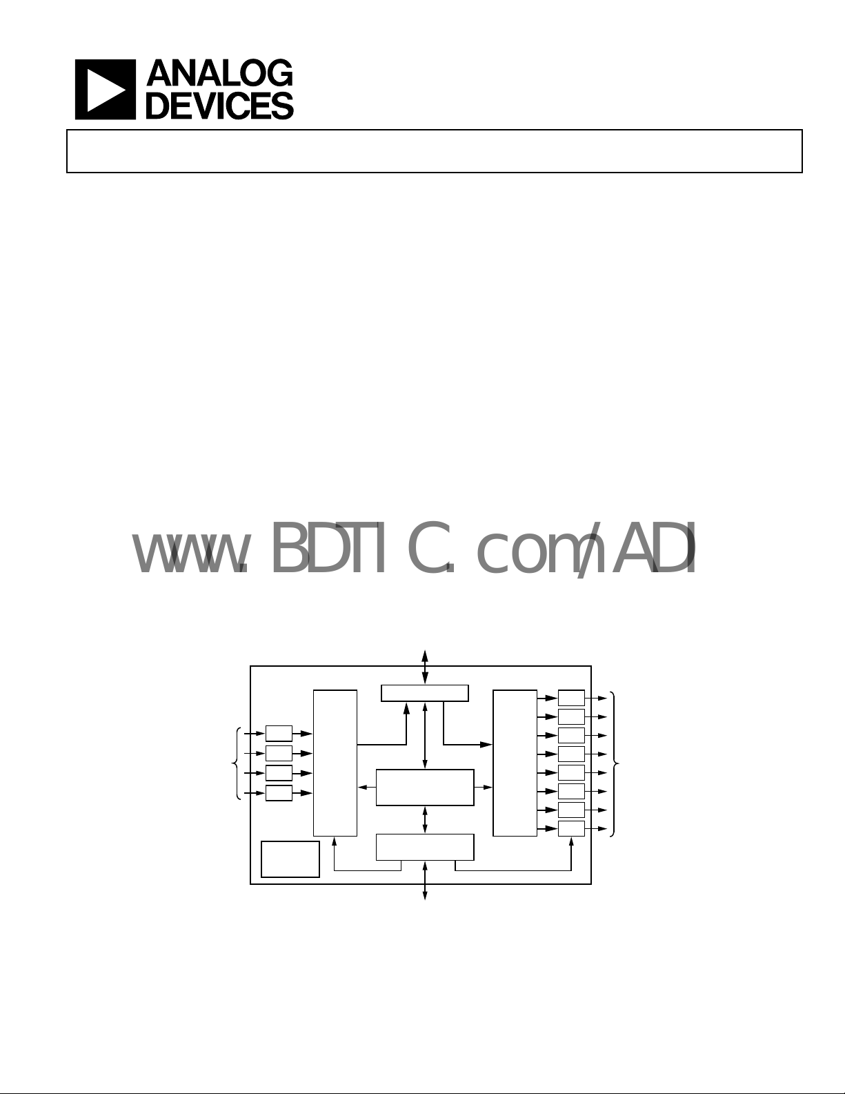
FUNCTIONAL BLOCK DIAGRAM
DIGITAL AUDIO
INPUT/OUTPUT
AD1937
ADC
NALOG
AUDIO
INPUTS
ADC
ADC
ADC
PRECISION
VOLTAGE
REFERENCE
DIGITAL
FILTER
Rev. 0
Information furnished by Analog Devices is believed to be accurate and reliable. However, no
responsibility is assumed by Analog Devices for its use, nor for any infringements of patents or other
rights of third parties that may result from its use. Specifications subject to change without notice. No
license is granted by implication or otherwise under any patent or patent rights of Analog Devices.
Trademarks and registered trademarks are the property of their respective owners.
SERIAL DATA PORT
SDATA
OUT
TIMING MANAGEMENT
AND CONTROL
(CLOCK AND PLL )
CONTROL PORT
CONTROL DAT A
INPUT/OUTPUT
DAC
SDATA
IN
CLOCKS
I2C
Figure 1.
One Technology Way, P.O. Box 9106, Norwood, MA 02062-9106, U.S.A.
Tel: 781.329.4700 www.analog.com
Fax: 781.461.3113 ©2008 Analog Devices, Inc. All rights reserved.
DIGITAL
FILTER
AND
VOLUME
CONTROL
DAC
DAC
DAC
DAC
DAC
DAC
DAC
ANALOG
AUDIO
OUTPUTS
07414-001
Page 2

AD1937
www.BDTIC.com/ADI
TABLE OF CONTENTS
Features .............................................................................................. 1
Applications ....................................................................................... 1
General Description ......................................................................... 1
Functional Block Diagram .............................................................. 1
Revision History ............................................................................... 2
Specifications ..................................................................................... 3
Test Conditions ............................................................................. 3
Analog Performance Specifications ........................................... 3
Crystal Oscillator Specifications................................................. 5
Digital Specifications ................................................................... 6
Power Supply Specifications........................................................ 6
Digital Filters ................................................................................. 7
Timing Specifications .................................................................. 8
Timing Diagrams .......................................................................... 9
Absolute Maximum Ratings .......................................................... 10
Thermal Resistance .................................................................... 10
ESD Caution ................................................................................ 10
Pin Configuration and Function Descriptions ........................... 11
Typical Performance Characteristics ........................................... 13
Theory of Operation ...................................................................... 15
Analog-to-Digital Converters (ADCs) .................................... 15
Digital-to-Analog Converters (DACs) .................................... 15
Clock Signals ............................................................................... 15
Reset and Power-Down ............................................................. 16
I2C Control Port .......................................................................... 16
Power Supply and Voltage Reference ....................................... 18
Serial Data Ports—Data Format ............................................... 19
Time-Division Multiplexed (TDM) Modes ............................ 20
Daisy-Chain Mode ..................................................................... 23
Additional Modes ....................................................................... 26
Control Registers ............................................................................ 27
Definitions ................................................................................... 27
PLL and Clock Control Registers ............................................. 27
DAC Control Registers .............................................................. 28
ADC Control Registers .............................................................. 30
Applications Circuits ...................................................................... 32
Outline Dimensions ....................................................................... 33
Ordering Guide .......................................................................... 33
REVISION HISTORY
9/08—Revision 0: Initial Version
Rev. 0 | Page 2 of 36
Page 3
AD1937
www.BDTIC.com/ADI
SPECIFICATIONS
TEST CONDITIONS
Performance of all channels is identical, exclusive of the interchannel gain mismatch and interchannel phase deviation specifications.
Table 1.
Parameter Value
Supply Voltages (AVDD, DVDD) 3.3 V
Temperature As specified in Table 2 and Table 3
Master Clock 12.288 MHz (48 kHz fS, 256 × fS mode)
Input Sample Rate 48 kHz
Measurement Bandwidth 20 Hz to 20 kHz
Word Width 24 bits
Load Capacitance (Digital Output) 20 pF
Load Current (Digital Output) ±1 mA or 1.5 kΩ to ½ DVDD supply
Input Voltage High 2.0 V
Input Voltage Low 0.8 V
ANALOG PERFORMANCE SPECIFICATIONS
Specifications guaranteed at a TA of 25°C.
Table 2.
Parameter Conditions/Comments Min Typ Max Unit
ANALOG-TO-DIGITAL CONVERTERS
ADC Resolution All ADCs 24 Bits
Dynamic Range 20 Hz to 20 kHz, −60 dB input
No Filter (RMS) 96 102 dB
With A-Weighted Filter (RMS) 98 105 dB
Total Harmonic Distortion + Noise −1 dBFS −96 −87 dB
Full-Scale Input Voltage (Differential) 1.9 V rms
Gain Error −10 +10 %
Interchannel Gain Mismatch −0.25 +0.25 dB
Offset Error −10 0 +10 mV
Gain Drift 100 ppm/°C
Interchannel Isolation −110 dB
CMRR 100 mV rms, 1 kHz 55 dB
100 mV rms, 20 kHz 55 dB
Input Resistance 14 kΩ
Input Capacitance 10 pF
Input Common-Mode Bias Voltage 1.5 V
DIGITAL-TO-ANALOG CONVERTERS
DAC Resolution All DACs 24 Bits
Dynamic Range 20 Hz to 20 kHz, −60 dB input
No Filter (RMS) 102 107 dB
With A-Weighted Filter (RMS) 105 110 dB
With A-Weighted Filter (Average) 112 dB
Rev. 0 | Page 3 of 36
Page 4
AD1937
www.BDTIC.com/ADI
Parameter Conditions/Comments Min Typ Max Unit
Total Harmonic Distortion + Noise 0 dBFS
Two channels running −94 dB
Eight channels running −86 −76 dB
Full-Scale Output Voltage 1.76 (4.96) V rms (V p-p)
Gain Error −10 +10 %
Interchannel Gain Mismatch −0.2 +0.2 dB
Offset Error −25 −6 +25 mV
Gain Drift −30 +30 ppm/°C
Interchannel Isolation 100 dB
Interchannel Phase Deviation 0 Degrees
Volume Control Step 0.375 dB
Volume Control Range 95 dB
De-emphasis Gain Error ±0.6 dB
Output Resistance at Each Pin 100 Ω
REFERENCE
Internal Reference Voltage FILTR pin 1.50 V
External Reference Voltage FILTR pin 1.32 1.50 1.68 V
Common-Mode Reference Output CM pin 1.50 V
REGULATOR
Input Supply Voltage VSUPPLY pin 4.5 5 5.5 V
Regulated Output Voltage VSENSE pin 3.19 3.37 3.55 V
Rev. 0 | Page 4 of 36
Page 5
AD1937
www.BDTIC.com/ADI
Specifications measured at a TC of 130°C.
Table 3.
Parameter Conditions/Comments Min Typ Max Unit
ANALOG-TO-DIGITAL CONVERTERS
ADC Resolution All ADCs 24 Bits
Dynamic Range 20 Hz to 20 kHz, −60 dB input
No Filter (RMS) 93 102 dB
With A-Weighted Filter (RMS) 96 104 dB
Total Harmonic Distortion + Noise −1 dBFS −96 −87 dB
Full-Scale Input Voltage (Differential) 1.9 V rms
Gain Error −10 +10 %
Interchannel Gain Mismatch −0.25 +0.25 dB
Offset Error −10 0 +10 mV
DIGITAL-TO-ANALOG CONVERTERS
DAC Resolution All DACs 24 Bits
Dynamic Range 20 Hz to 20 kHz, −60 dB input
No Filter (RMS) 101 107 dB
With A-Weighted Filter (RMS) 104 110 dB
With A-Weighted Filter (Average) 112 dB
Total Harmonic Distortion + Noise 0 dBFS
Two channels running −94 dB
Eight channels running −86 −70 dB
Full-Scale Output Voltage 1.76 (4.96) V rms (V p-p)
Gain Error −10 +10 %
Interchannel Gain Mismatch −0.2 +0.2 dB
Offset Error −25 −6 +25 mV
Gain Drift −30 +30 ppm/°C
REFERENCE
Internal Reference Voltage FILTR pin 1.50 V
External Reference Voltage FILTR pin 1.32 1.50 1.68 V
Common-Mode Reference Output CM pin 1.50 V
REGULATOR
Input Supply Voltage VSUPPLY pin 4.5 5 5.5 V
Regulated Output Voltage VSENSE pin 3.2 3.43 3.65 V
CRYSTAL OSCILLATOR SPECIFICATIONS
Table 4.
Parameter Min Typ Max Unit
Transconductance 3.5 mmhos
Rev. 0 | Page 5 of 36
Page 6
AD1937
www.BDTIC.com/ADI
DIGITAL SPECIFICATIONS
−40°C < TA < +130°C, DVDD = 3.3 V ± 10%.
Table 5.
Parameter Conditions/Comments Min Typ Max Unit
INPUT
High Level Input Voltage (VIH) 2.0 V
MCLKI/MCLKXI pin 2.2 V
Low Level Input Voltage (VIL) 0.8 V
Input Leakage IIH @ VIH = 2.4 V 10 μA
I
Input Capacitance 5 pF
OUTPUT
High Level Output Voltage (VOH) IOH = 1 mA DVDD − 0.60 V
Low Level Output Voltage (VOL) IOL = 1 mA 0.4 V
POWER SUPPLY SPECIFICATIONS
Table 6.
Parameter Conditions/Comments Min Typ Max Unit
SUPPLIES
Voltage DVDD 3.0 3.3 3.6 V
AVDD 3.0 3.3 3.6 V
VSUPPLY 4.5 5.0 5.5 V
Digital Current Master clock = 256 f
Normal Operation fS = 48 kHz 56 mA
f
f
Power-Down fS = 48 kHz to 192 kHz 2.0 mA
Analog Current
Normal Operation 74 mA
Power-Down 23 mA
DISSIPATION
Operation Master clock = 256 fS, 48 kHz
All Supplies 429 mW
Digital Supply 185 mW
Analog Supply 244 mW
Power-Down, All Supplies 83 mW
POWER SUPPLY REJECTION RATIO
Signal at Analog Supply Pins 1 kHz, 200 mV p-p 50 dB
20 kHz, 200 mV p-p 50 dB
@ VIL = 0.8 V 10 μA
IL
S
= 96 kHz 65 mA
S
= 192 kHz 95 mA
S
Rev. 0 | Page 6 of 36
Page 7
AD1937
www.BDTIC.com/ADI
DIGITAL FILTERS
Table 7.
Parameter Mode Factor Min Typ Max Unit
ADC DECIMATION FILTER
Pass Band 0.4375 × f
All modes, typical @ 48 kHz
S
Pass-Band Ripple ±0.015 dB
Transition Band 0.5 × f
Stop Band 0.5625 × f
S
S
Stop-Band Attenuation 79 dB
Group Delay 22.9844 ÷ f
DAC INTERPOLATION FILTER
Pass Band 48 kHz mode, typical @ 48 kHz 0.4535 × f
96 kHz mode, typical @ 96 kHz 0.3646 × f
192 kHz mode, typical @ 192 kHz 0.3646 × f
S
S
S
Pass-Band Ripple 48 kHz mode, typical @ 48 kHz ±0.01 dB
96 kHz mode, typical @ 96 kHz ±0.05 dB
192 kHz mode, typical @ 192 kHz ±0.1 dB
Transition Band 48 kHz mode, typical @ 48 kHz 0.5 × f
96 kHz mode, typical @ 96 kHz 0.5 × f
192 kHz mode, typical @ 192 kHz 0.5 × f
Stop Band 48 kHz mode, typical @ 48 kHz 0.5465 × f
96 kHz mode, typical @ 96 kHz 0.6354 × f
192 kHz mode, typical @ 192 kHz 0.6354 × f
S
S
S
S
S
S
Stop-Band Attenuation 48 kHz mode, typical @ 48 kHz 70 dB
96 kHz mode, typical @ 96 kHz 70 dB
192 kHz mode, typical @ 192 kHz 70 dB
Group Delay 48 kHz mode, typical @ 48 kHz 25 ÷ f
96 kHz mode, typical @ 96 kHz 11 ÷ f
192 kHz mode, typical @ 192 kHz 8 ÷ f
S
S
S
21 kHz
24 kHz
27 kHz
479 μs
S
22 kHz
35 kHz
70 kHz
24 kHz
48 kHz
96 kHz
26 kHz
61 kHz
122 kHz
521 μs
115 μs
42 μs
Rev. 0 | Page 7 of 36
Page 8
AD1937
www.BDTIC.com/ADI
TIMING SPECIFICATIONS
−40°C < TA < +130°C, DVDD = 3.3 V ± 10%.
Table 8.
Parameter Condition Comments Min Max Unit
INPUT MASTER CLOCK (MCLK) AND RESET
tMH MCLK duty cycle
t
MH
f
MCLK frequency PLL mode, 256 fS reference 6.9 13.8 MHz
MCLK
f
MCLK
t
PDR
t
PDRR
PLL
Lock Time MCLK or LRCLK 10 ms
256 fS VCO Clock, Output Duty Cycle,
MCLKO/MCLKXO Pin
I2C See Figure 13 and Figure 14
f
SCL clock frequency 400 kHz
SCL
t
SCL low 1.3 μs
SCLL
t
SCL high 0.6 μs
SCLH
t
Setup time (start condition) Relevent for repeated start condition 0.6 μs
SCS
t
Hold time (start condition) First clock generated after this period 0.6 μs
SCH
t
Setup time (stop condition) 0.6 μs
SSH
tDS Data setup time 100 ns
tSR SDA and SCL rise time 300 ns
tSF SDA and SCL fall time 300 ns
t
Bus-free time Between stop and start 1.3 μs
BFT
DAC SERIAL PORT See Figure 2
t
DBH
t
DBL
t
DLS
DLRCLK skew From DBCLK falling, master mode −8 +8 ns
t
DLH
t
DDS
t
DDH
ADC SERIAL PORT See Figure 3
t
ABH
t
ABL
t
ALRCLK setup To ABCLK rising, slave mode 10 ns
ALS
ALRCLK skew From ABCLK falling, master mode −8 +8 ns
t
ALH
t
ABDD
AUXILIARY INTERFACE
t
AXDS
t
AXDH
t
DXDD
t
XBH
t
XBL
t
DLS
t
DLH
DAC/ADC clock source = PLL clock
, 384 fS, 512 fS, and 768 f
@ 256 f
S
DAC/ADC clock source = direct MCLK
(bypass on-chip PLL)
@ 512 f
S
S
40 60 %
40 60 %
Direct 512 fS mode 27.6 MHz
Low 15 ns
Recovery Reset to active output 4096 t
MCLK
40 60 %
DBCLK high Slave mode 10 ns
DBCLK low Slave mode 10 ns
DLRCLK setup To DBCLK rising, slave mode 10 ns
DLRCLK hold From DBCLK rising, slave mode 5 ns
DS DATA setup To D BCLK rising 10 n s
DSDATA hold From DBCLK rising 5 ns
ABCLK high Slave mode 10 ns
ABCLK low Slave mode 10 ns
ALRCLK hold From ABCLK rising, slave mode 5 ns
ASDATA delay From ABCLK falling, any mode 18 ns
AAUXDATA s etu p To AU XBCLK rising 10 n s
AAUXDATA hold From AUXBCLK rising 5 ns
DAUXDATA delay From AUXBCLK falling 18 ns
AUXBCLK high 10 ns
AUXBCLK low 10 ns
AUXLRCLK setup To AUXBCLK rising 10 ns
AUXLRCLK hold From AUXBCLK rising 5 ns
Rev. 0 | Page 8 of 36
Page 9
AD1937
www.BDTIC.com/ADI
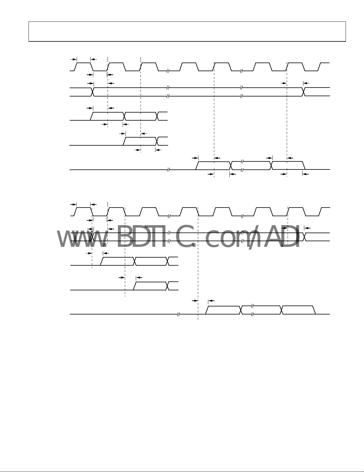
TIMING DIAGRAMS
t
DBH
DBCLK
t
DBL
t
DDS
t
DLH
t
DDH
t
ALH
07414-025
LEFT-JUSTIFIED
2
I
S-JUSTIFIED
RIGHT-JUST IFIED
DLRCLK
DSDATAx
MODE
DSDATAx
MODE
DSDATAx
MODE
ABCLK
ALRCLK
t
ABH
t
DLS
t
DDS
MSB
t
DDH
MSB – 1
t
DDS
MSB
t
DDH
t
DDS
MSB LSB
t
DDH
Figure 2. DAC Serial Timing
t
ABL
t
ALS
LEFT-JUSTIFIED
2
I
S-JUSTIFIED
RIGHT-JUST IFIED
ASDATAx
MODE
ASDATAx
MODE
ASDATAx
MODE
t
ABDD
MSB
t
ABDD
MSB – 1
MSB
Figure 3. ADC Serial Timing
t
ABDD
MSB
LSB
7414-026
Rev. 0 | Page 9 of 36
Page 10
AD1937
www.BDTIC.com/ADI
ABSOLUTE MAXIMUM RATINGS
Table 9.
Parameter Rating
Analog (AVDD) −0.3 V to +3.6 V
Digital (DVDD) −0.3 V to +3.6 V
VSUPPLY −0.3 V to +6.0 V
Input Current (Except Supply Pins) ±20 mA
Analog Input Voltage (Signal Pins) –0.3 V to AVDD + 0.3 V
Digital Input Voltage (Signal Pins) −0.3 V to DVDD + 0.3 V
Operating Temperature Range (Case) −40°C to +125°C
Storage Temperature Range −65°C to +150°C
Stresses above those listed under Absolute Maximum Ratings
may cause permanent damage to the device. This is a stress
rating only; functional operation of the device at these or any
other conditions above those indicated in the operational
section of this specification is not implied. Exposure to absolute
maximum rating conditions for extended periods may affect
device reliability.
THERMAL RESISTANCE
θJA represents junction-to-ambient thermal resistance;
represents the junction-to-case thermal resistance.
θ
JC
All characteristics are for a 4-layer board.
Table 10.
Package Type θ
64-Lead LQFP 47 11.1 °C/W
JA
θ
JC
Unit
ESD CAUTION
Rev. 0 | Page 10 of 36
Page 11
AD1937
www.BDTIC.com/ADI
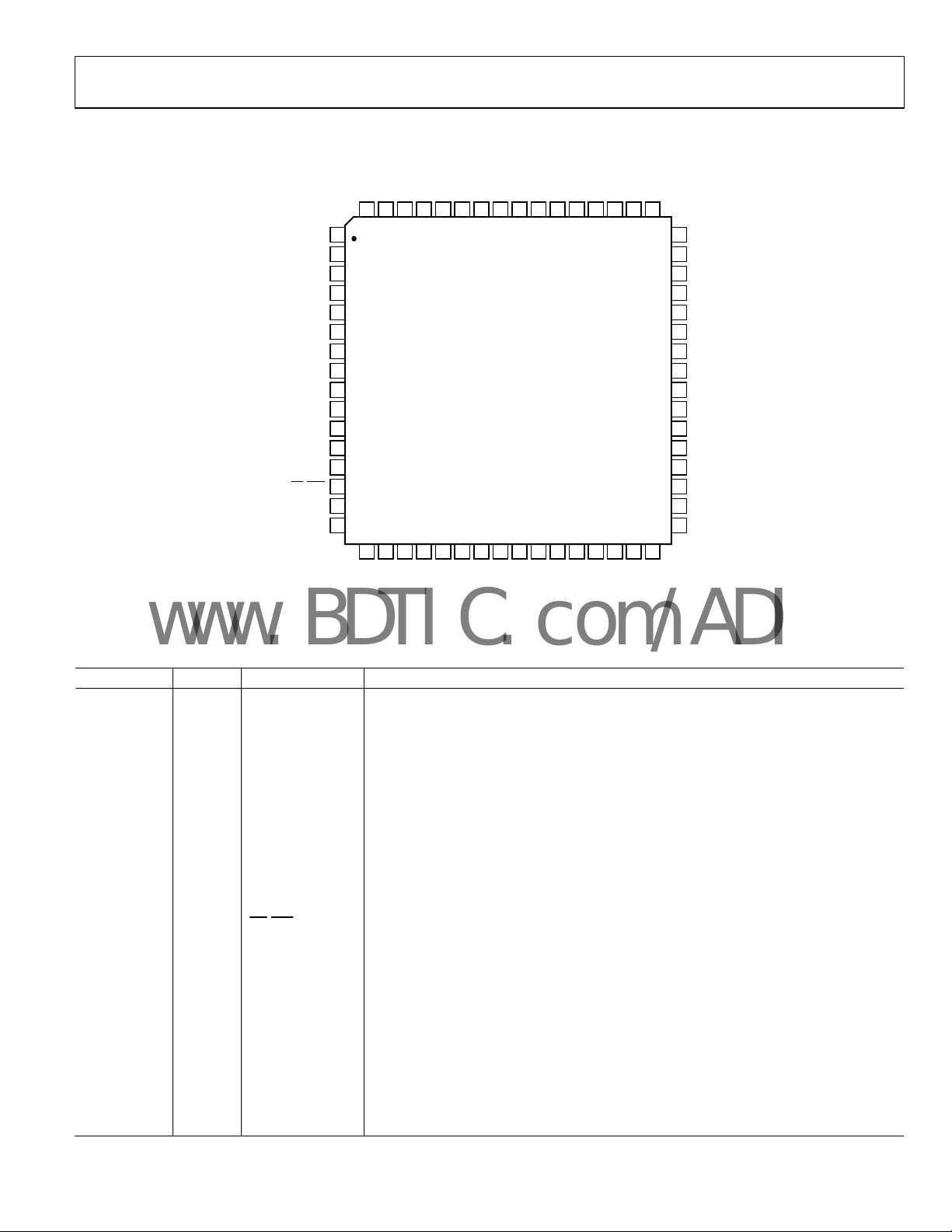
PIN CONFIGURATION AND FUNCTION DESCRIPTIONS
AGND
MCLKI/MCL KXI
MCLKO/MCLKXO
AGND
AVDD
DAC3LP
DAC3LN
DAC3RP
DAC3RN
DAC4LP
DAC4LN
DAC4RP
DAC4RN
PD/RST
DSDATA4
DGND
NC = NO CONNECT
NC64NC63AVDD62LF61ADC2RN60ADC2RP59ADC2LN58ADC2LP57ADC1RN56ADC1RP55ADC1LN54ADC1LP53CM52AVDD51NC50NC
1
2
3
4
5
6
7
8
9
10
11
12
13
14
15
16
17
DVDD
20
DSDATA318DSDATA219DSDATA1
21
AD1937
TOP VIEW
(Not to Scale)
DIFFERENTIAL OUTPUT
22
23
24
25
DBCLK
DLRCLK
VDRIVE
VSENSE
VSUPPLY
ASDATA226ASDATA1
27
28
ABCLK
Figure 4. Pin Configuration
49
48
AGND
47
FILTR
46
AGND
45
AVDD
44
AGND
43
DAC2RN
42
DAC2RP
41
DAC2LN
40
DAC2LP
39
DAC1RN
38
DAC1RP
37
DAC1LN
36
DAC1LP
35
ADDR1
34
SCL
33
DGND
29
30
31
32
SDA
DVDD
ADDR0
ALRCLK
07414-002
Table 11. Pin Function Descriptions
Pin No. Type
1
Mnemonic Description
1, 4, 44, 46, 48 I AGND Analog Ground.
2 I MCLKI/MCLKXI Master Clock Input/Crystal Oscillator Input.
3 O MCLKO/MCLKXO Master Clock Output/Crystal Oscillator Output.
5, 45, 51, 62 I AVDD Analog Power Supply. Connect this pin to analog 3.3 V supply.
6 O DAC3LP DAC3 Left Positive Output.
7 O DAC3LN DAC3 Left Negative Output.
8 O DAC3RP DAC3 Right Positive Output.
9 O DAC3RN DAC3 Right Negative Output.
10 O DAC4LP DAC4 Left Positive Output.
11 O DAC4LN DAC4 Left Negative Output.
12 O DAC4RP DAC4 Right Positive Output.
13 O DAC4RN DAC4 Right Negative Output
14 I
PD
/RST
15 I/O DSDATA4
Power-Down Reset (Active Low).
DAC Serial Data Input 4. Data input to DAC4 data in/TDM DAC2 data out (dual-line mode)/
AUX DAC2 data out (to external DAC2).
16, 33 I DGND Digital Ground.
17, 32 I DVDD Digital Power Supply. Connect this pin to digital 3.3 V supply.
18 I/O DSDATA3
DAC Serial Data Input 3. Data input to DAC3 data in/TDM DAC2 data in (dual-line mode)/AUX
ADC2 data in (from external ADC2).
19 I/O DSDATA2
DAC Serial Data Input 2. Data input to DAC2 data in/TDM DAC data out/AUX ADC1 data in
(from external ADC1).
20 I DSDATA1 DAC Serial Data Input 1. Data input to DAC1 data in/TDM DAC data in/TDM data in.
21 I/O DBCLK Bit Clock for DACs. Can be programmed as input or output in all modes.
22 I/O DLRCLK Frame Clock for DACs. Can be programmed as input or output in all modes.
Rev. 0 | Page 11 of 36
Page 12

AD1937
www.BDTIC.com/ADI
Pin No. Type
23 I VSUPPLY 5 V Input to Regulator, Emitter of Pass Transistor.
24 I VSENSE Connect 3.3 V Regulator Output, Collector of Pass Transistor, to This Pin.
25 O VDRIVE Drive for Base of Pass Transistor.
26 I/O ASDATA2
27 O ASDATA1 ADC Serial Data Output 1. Data Output from ADC1/TDM ADC data out/TDM data out.
28 I/O ABCLK Bit Clock for ADCs. Can be programmed as input or output in all modes.
29 I/O ALRCLK Frame Clock for ADCs. Can be programmed as input or output in all modes.
30 I ADDR0 I2C Address Assignment.
31 I/O SDA Control Data Port (I2C).
34 I SCL Control Clock Port (I2C).
35 I ADDR1 I2C Address Assignment.
36 O DAC1LP DAC1 Left Positive Output.
37 O DAC1LN DAC1 Left Negative Output.
38 O DAC1RP DAC1 Right Positive Output.
39 O DAC1RN DAC1 Right Negative Output.
40 O DAC2LP DAC2 Left Positive Output.
41 O DAC2LN DAC2 Left Negative Output.
42 O DAC2RP DAC2 Right Positive Output.
43 O DAC2RN DAC2 Right Negative Output.
47 O FILTR Analog Voltage Reference Filter Capacitor Connection. Bypass with 10 μF||100 nF to AGND.
49, 50, 63, 64 NC No Connect.
52 O CM Common-Mode Reference Filter Capacitor Connection. Bypass with 47 μF||100 nF to AGND.
53 I ADC1LP ADC1 Left Positive Input.
54 I ADC1LN ADC1 Left Negative Input.
55 I ADC1RP ADC1 Right Positive Input.
56 I ADC1RN ADC1 Right Negative Input.
57 I ADC2LP ADC2 Left Positive Input.
58 I ADC2LN ADC2 Left Negative Input.
59 I ADC2RP ADC2 Right Positive Input.
60 I ADC2RN ADC2 Right Negative Input.
61 O LF PLL Loop Filter, Return to AVDD.
1
I = input, O = output.
1
Mnemonic Description
ADC Serial Data Output 2. Data Output from ADC2/TDM ADC data in/AUX DAC1 data out (to
external DAC1).
Rev. 0 | Page 12 of 36
Page 13

AD1937
www.BDTIC.com/ADI
TYPICAL PERFORMANCE CHARACTERISTICS
0.10
0.08
0.06
0.04
0.02
0
–0.02
MAGNITUDE (d B)
–0.04
–0.06
–0.08
–0.10
01161412108642
FREQUENCY (kHz)
Figure 5. ADC Pass-Band Filter Response, 48 kHz
8
07414-003
0
–50
MAGNITUDE (d B)
–100
–150
0412 24 36
FREQUENCY (kHz)
Figure 8. DAC Stop-Band Filter Response, 48 kHz
8
07414-006
0
–10
–20
–30
–40
–50
–60
MAGNITUDE (d B)
–70
–80
–90
–100
045 101520253035
FREQUENCY (kHz)
Figure 6. ADC Stop-Band Filter Response, 48 kHz
0.06
0.04
0.02
0
MAGNITUDE (d B)
–0.02
0.10
0.05
0
MAGNITUDE (d B)
–0.05
0
07414-004
–0.10
09724824
Figure 9. DAC Pass-Band Filter Response, 96 kHz
0
–50
MAGNITUDE (d B)
–100
FREQUENCY (kHz)
6
07414-007
–0.04
–0.06
02168
FREQUENCY (kHz)
Figure 7. DAC Pass-Band Filter Response, 48 kHz
4
07414-005
–150
0924 48 72
Figure 10. DAC Stop-Band Filter Response, 96 kHz
Rev. 0 | Page 13 of 36
FREQUENCY (kHz)
6
07414-008
Page 14

AD1937
www.BDTIC.com/ADI
0.5
0.4
0.3
0.2
0.1
0
–0.1
MAGNITUDE (dB)
–0.2
–0.3
–0.4
–0.5
0681632
FREQUENCY (kHz)
4
07414-009
Figure 11. DAC Pass-Band Filter Response, 192 kHz
0
–2
–4
–6
MAGNITUDE (d B)
–8
–10
48 9664 80
FREQUENCY (kHz)
Figure 12. DAC Stop-Band Filter Response, 192 kHz
07414-010
Rev. 0 | Page 14 of 36
Page 15

AD1937
www.BDTIC.com/ADI
THEORY OF OPERATION
ANALOG-TO-DIGITAL CONVERTERS (ADCs)
There are four ADC channels in the AD1937 configured as two
stereo pairs with differential inputs. The ADCs can operate at a
nominal sample rate of 48 kHz, 96 kHz, or 192 kHz. The ADCs
include on-board digital antialiasing filters with 79 dB stopband attenuation and linear phase response, operating at an
oversampling ratio of 128 (48 kHz, 96 kHz, and 192 kHz modes).
Digital outputs are supplied through two serial data output
pins (one for each stereo pair): a common frame clock (ALRCLK)
and a common bit clock (ABCLK). Alternatively, the TDM
modes can be used to access up to 16 channels on a single
TDM data line.
The ADCs must be driven from a differential signal source for
best performance. The input pins of the ADCs connect to internal
switched capacitors. To isolate the external driving op amp from
the glitches caused by the internal switched capacitors, each
input pin should be isolated by using a series-connected external
100 Ω resistor and a 1 nF capacitor connected from each input
to ground. Use a high quality capacitor such as a ceramic
NP0/C0G, or polypropylene film.
The differential inputs have a nominal common-mode voltage
of 1.5 V. The voltage at the common-mode reference pin (CM)
can be used to bias external op amps to buffer the input signals
(see the Power Supply and Voltage Reference section). The
inputs can also be ac-coupled and in that case do not need
an external dc bias to CM.
A digital high-pass filter can be switched in line with the
ADCs (ADC Control 0 Register) to remove residual dc offsets.
It has a 1.4 Hz, 6 dB per octave cutoff at a 48 kHz sample rate.
The cutoff frequency scales directly with sample frequency.
DIGITAL-TO-ANALOG CONVERTERS (DACs)
The AD1937 DAC channels are arranged in four stereo pairs,
giving eight analog outputs; the outputs are differential for
improved noise and distortion performance. The DACs include
on-board digital reconstruction filters with 70 dB stop-band
attenuation and linear phase response, operating at an oversampling ratio of 4 (48 kHz or 96 kHz modes) or 2 (192 kHz
mode). Each channel has its own independently programmable
attenuator, adjustable in 255 steps in increments of 0.375 dB.
Digital inputs are supplied through four serial data input pins
(one for each stereo pair), a common frame clock (DLRCLK),
and a common bit clock (DBCLK). Alternatively, one of the
TDM modes can be used to access up to 16 channels on a
single TDM data line.
Each output pin has a nominal common-mode dc level of 1.5 V
and swings ±1.27 V for a 0 dBFS digital input signal. A single
op amp, third-order, external, low-pass filter is recommended
to remove high frequency noise present on the output pins, as
well as to provide a differential-to-single-ended conversion for
the differential output. Note that the use of op amps with low
slew rates or low bandwidth can cause high frequency noise
and tones to fold down into the audio band; exercise care in
selecting these components.
The voltage at CM can be used to bias the external op amps that
buffer the output signals (see the Power Supply and Voltage
Reference section).
CLOCK SIGNALS
The on-chip phase-locked loop (PLL) can be selected to reference the input sample rate from either of the LRCLK pins
or 256×, 384×, 512×, or 768× sample rate s (f
the 48 kHz mode from the MCLKI/MCLKXI pin. The default at
power-up is 256 × f
mode, the master clock frequency stays at the same absolute
frequency; therefore, the actual multiplication rate is divided
by 2. In 192 kHz mode, the actual multiplication rate is divided
by 4. For example, if the AD1937 is programmed in 256 × f
mode, the frequency of the master clock input is 256 × 48 kHz
= 12.288 MHz. If the AD1937 is then switched to 96 kHz
operation (by writing to the I
master clock should remain at 12.288 MHz, which is 128 × f
in this example. In 192 kHz mode, this becomes 64 × f
The internal clock for the ADCs is 256 × f
The internal clock for the DACs varies by mode: 512 × f
mode), 256 × f
default, the on-board PLL generates this internal master clock
from an external clock. A direct 512 × f
mode) master clock can be used for either the ADCs or DACs,
if selected in the PLL and Clock Control 1 register.
Note that it is not possible to use a direct clock for the ADCs
set to the 192 kHz mode. It is required that the on-chip PLL
be used in this mode.
The PLL can be powered down in the PLL and Clock Control 0
Register. To ensure reliable locking when changing PLL modes,
or if the reference clock is unstable at power-on, power down
the PLL and then power it back up after the reference clock has
stabilized.
The internal master clock (MCLK) can be disabled in the
PLL and Clock Control 0 register to reduce power dissipation
when the AD1937 is idle. The clock should be stable before it
is enabled. Unless a standalone mode is selected (see the I
Control Port section), the clock is disabled by reset and must
be enabled by writing to the I
from the MCLKI/MCLKXI pin. In 96 kHz
S
2
C port), the frequency of the
(96 kHz mode), or 128 × fS (192 kHz mode). By
S
2
C port for normal operation.
), referenced to
S
S
S
.
S
for all clock modes.
S
(48 kHz
S
(referenced to 48 kHz
S
2
C
Rev. 0 | Page 15 of 36
Page 16

AD1937
www.BDTIC.com/ADI
To maintain the highest performance possible, limit the clock jitter
of the internal master clock signal to less than a 300 ps rms time
interval error (TIE). Even at these levels, extra noise or tones
can appear in the DAC outputs if the jitter spectrum contains
large spectral peaks. If the internal PLL is not used, it is best to
use an independent crystal oscillator to generate the master clock.
In addition, it is especially important that the clock signal not
pass through an FPGA, CPLD, or other large digital chip (such
as a DSP) before being applied to the AD1937. In most cases,
this induces clock jitter due to the sharing of common power
and ground connections with other unrelated digital output
signals. When the PLL is used, jitter in the reference clock is
attenuated above a certain frequency depending on the loop filter.
RESET AND POWER-DOWN
The function of the PD/
their default settings. To avoid audio pops,
power down the analog outputs. After
and the PLL acquires lock condition, an initialization routine
runs inside the AD1937. This initialization lasts for approx-
imately 256 master clock cycles. Once the routine is complete,
the registers can be programmed.
The power-down bits in the PLL and Clock Control 0, DAC
Control 1, and ADC Control 1 registers power down their
respective sections. All other register settings are retained.
To guarantee proper startup, the
pulled low by an external resistor.
RST
pin sets all the control registers to
PD
RST
/
does not
PD
RST
/
is deasserted
PD
RST
/
pin should be
I2C CONTROL PORT
The AD1937 has an I2C-compatible control port that permits
programming and reading back the internal control registers
for the ADCs, DACs, and clock system. There is also a standalone mode available for operation without serial control,
configured at reset using the serial control pins. All registers
are set to default except internal MCLK enable, which is set to
1 and ADC BCLK and LRCLK master/slave is set by SDA (see
Tabl e 12 for details).
Table 12. Hardware Selection of Standalone Mode
ADDR0
ADC Clocks
Slave 0 0 0 0
Master 0 1 0 0
(Pin 30)
SDA
(Pin 31)
SCL
(Pin 34)
ADDR1
(Pin 35)
2
C interface of the AD1937 is a 2-wire interface that
The I
consists of a clock line (SCL) and a data line (SDA). SDA
is bidirectional and the AD1937 drives SDA either to acknowledge the master (ACK) or to send data during a read operation.
The SDA pin for the I
requires a 2 kΩ pull-up resistor. A write or read access occurs
when the SDA line is pulled low while the SCL line is high,
indicated by start in the timing diagrams. SDA is only allowed
to change when SCL is low except when a start or stop condition
occurs, as shown in Figure 13 and Figure 14. The first eight bits
of the data-word consist of the device address and the R/
The device address consists of an internal built-in address
(0x08) OR’ed with the two address bits, ADDR1 and ADDR0,
and the R/
used in a system. Tie I
program the ADDR bits accordingly as 0 or 1. Initiating a write
operation to the AD1937 involves sending a start condition and
then sending the device address with the R/
AD1937 responds by issuing an acknowledge to indicate that it
has been addressed. The user then sends a second frame telling
the AD1937 which register is required to be written to. Another
acknowledge is issued by the AD1937. Finally, the user can send
another frame with the eight data bits required to be written to
the register. A third acknowledge is issued by the AD1937 after
which the user can send a stop condition to complete the data
transfer.
A read operation requires that the user first write to the
AD1937 to point to the correct register and then read the
data. This is achieved by sending a start condition followed
by the device address frame, with the R/
returns an acknowledge. The master then sends the register
address frame. Following the acknowledge from the AD1937,
the user must issue a repeated start condition. The next frame
is the device address with the R/
returns an acknowledge. On the next frame, the AD1937
outputs the register data on the SDA line; the master should
send an acknowledge. A stop condition completes the read
operation. and show examples of writing
to and reading from the DAC1L volume control register,
Address 0x06 (see ).
W
bit. The two address bits allow four AD1937s to be
Figure 13 Figure 14
2
C port is an open-drain collector and
2
C ADDR0 and ADDR1 low or high and
W
bit set low. The
W
bit low; the AD1937
W
bit set high; the AD1937
Table 2 8
W
bit.
Rev. 0 | Page 16 of 36
Page 17

AD1937
SCK
SDA
www.BDTIC.com/ADI
SCL
(CONTINUED)
SDA
(CONTINUED)
START BY
MASTER (S)
SCK
SDA
START BY
MASTER (S)
REPEATED START
BY MASTER (S)
00001
FRAME 1
CHIP ADDRESS BYTE
00001
FRAME 1
CHIP ADDRESS BYTE
0 000 1
FRAME 3
CHIP ADDRESS BYTE
ADDR1 ADDR0
SCK
(CONTINUED)
SDA
(CONTINUED)
ADDR1 ADDR0
ADDR1 ADDR 0
R/W 0 00 00 011
ACK. BY
AD1937 (AS)
D7 D6 D5 D4 D3 D2 D1 D0
Figure 13. I
2
C Write Format
R/W 0 00 00 011
ACK. BY
AD1937 (AS)
R/W
ACK. BY
AD1937 (AS)
DATA BYTE TO AD1937
D7 D6 D5 D4 D3 D2 D1 D0
FRAME 2
REGISTER ADDRESS BYTE
FRAME 3
REGISTER ADDRESS BYTE
REGISTER DAT A
Figure 14. I2C Read Format
FRAME 2
FRAME 4
ACK. BY
MASTER (AM)
MASTER (AM)
ACK. BY
MASTER (AM)
STOP BY
MASTER (P)
ACK. BY
AD1937 (AS)
ACK. BY
07414-011
STOP BY
MASTER (P)
07414-012
Rev. 0 | Page 17 of 36
Page 18

AD1937
www.BDTIC.com/ADI
Table 13. I2C Abbreviation Table
Abbreviation Condition
S Repeated start by master
P Stop by master
AM Acknowledge by master
AS Acknowledge by AD1937
Table 14. Single Word I
Chip Address, R/W = 0
S
Table 15. Burst Mode I
Chip Address, R/W = 0
S
Table 16. Single Word I
Chip Address, R/W = 0
S
Table 17. Burst Mode I
Chip Address,
S
R/W
= 0
POWER SUPPLY AND VOLTAGE REFERENCE
The AD1937 is designed for a 3.3 V supply. Separate power
supply pins are provided for the analog and digital sections.
To minimize noise pickup, these pins should be bypassed with
100 nF ceramic chip capacitors placed as close to the pins as
possible. A bulk aluminum electrolytic capacitor of at least
22 μF should also be provided on the same printed circuit
board (PCB) as the codec. For critical applications, improved
performance is obtained with separate supplies for the analog
and digital sections. If this is not possible, it is recommended
that the analog and digital load pins be isolated by means of a
ferrite bead in series with the supply. It is important that the
analog supply be as clean as possible.
The AD1937 includes a 3.3 V regulator driver that only requires
an external pass transistor, a resistor, and bypass capacitors to
turn a 5 V supply into 3.3 V. If the regulator driver is not used,
connect VSUPPLY, VDRIVE, and VSENSE to DGND.
All digital inputs are compatible with TTL and CMOS levels.
All outputs are driven from the 3.3 V DVDD supply and are
compatible with TTL and 3.3 V CMOS levels.
2
C Write
AS Register Address AS Data Word AS P
2
C Write
AS Register Address AS Data Word 1 AS Data Word 2 AS Data Word N AS P
2
C Read
2
C Read
AS
AS Register Address AS S
Register
Address
AS S
Chip Address,
= 1
R/W
Chip Address, R/W
Data
AS
Word 1
The ADC and DAC internal analog voltage reference (V
brought out on the FILTR pin and should be bypassed as close
as possible to the chip with a parallel combination of 10 μF and
100 nF capacitors. Any external current drawn should be limited
to less than 50 μA.
The internal reference can be disabled in the PLL and Clock
Control 1 register, and FILTR can be driven from an external
source. This can be used to scale the DAC output to the clipping
level of a power amplifier based on its power supply voltage.
The ADC input gain varies by the inverse ratio. It is not advisable
to drive the FILTR pin with more than (AVDD/2) V. The total
gain from ADC input to DAC output remains constant.
The CM pin should be bypassed as close as possible to the chip,
with a parallel combination of 47 μF and 100 nF capacitors. This
voltage can be used to bias external op amps to the common-mode
voltage of the input and output signal pins. The output current
should be limited to less than 0.5 mA source and 2 mA sink.
= 1
AM
Data
Word 2
Data Word AM P
AS
Data
AM
Word N
AM P
) is
REF
Rev. 0 | Page 18 of 36
Page 19

AD1937
A
A
A
A
www.BDTIC.com/ADI
SERIAL DATA PORTS—DATA FORMAT
The eight DAC channels use a common serial bit clock (DBCLK)
and a common left-right framing clock (DLRCLK) in the serial
data port. The four ADC channels use a common serial bit
clock (ABCLK) and left-right framing clock (ALRCLK) in the
serial data port. The clock signals are all synchronous with the
sample rate. The normal stereo serial modes are shown in
Figure 15.
The ADC and DAC serial data modes default to I
The ports can also be programmed for left-justified stereo,
right-justified stereo, and TDM modes. The word width is
2
S stereo.
24 bits by default and can be set to 16 or 20 bits in the DAC
Control 2 and ADC Control 1 registers. The DAC serial formats
are programmable in the DAC Control 0 register. The polarity of
DBCLK and DLRCLK is programmable in the DAC Control 1 register. The ADC serial format is programmable in ADC Control 1
register. The ABCLK and ALRCLK clock polarities are programmed in ADC Control 2 register. In Figure 2, Figure 3, and
Figure 15 all of the clocks are shown with their normal polarity.
Both DAC and ADC serial ports can be programmed to become
the bus masters according to DAC Control 1 and ADC Control 2
registers. By default, both ADC and DAC serial ports are in the
slave mode.
LRCLK
BCLK
SDAT
LRCLK
BCLK
SDAT
LRCLK
BCLK
SDAT
LRCLK
BCLK
SDAT
MSB MSB
MSB
MSB MSB
NOTES
1. DSP MODE DOES NOT IDENTIF Y CHANNEL.
2. LRCL K NORMAL LY OP ERATES AT
3. BCLK F REQUENCY IS NO RMALLY 64 × LRCL K BUT MAY BE OPE RATED IN BURST MO DE.
LEFT CHANNEL RIGHT CHANNEL
LSB LSB
LEFT-JUST IFIED MO DE—16 BITS T O 24 BITS PER CHANNEL
LEFT CHANNEL
LSB
I2S-JUSTIFI ED MODE—16 BITS TO 24 BIT S PER CHANNEL
LEFT CHANNEL RIGHT CHANNEL
MSB MSB
RIGHT-JUSTI FIED MODE—S ELECT NUMBER OF BITS PER CHANNEL
DSP MODE—16 BITS TO 24 BITS PER CHANNEL
f
EXCEPT FOR DSP MODE, WHICH IS 2 ×fS.
S
LSB LSB
LSB LSB
f
1/
S
Figure 15. Stereo Modes
MSB
RIGHT CHANNEL
LSB
07414-024
Rev. 0 | Page 19 of 36
Page 20

AD1937
A
A
www.BDTIC.com/ADI
TIME-DIVISION MULTIPLEXED (TDM) MODES
The serial ports of the AD1937 have several different TDM
serial data modes. Single-line TDM mode is the most commonly used configuration (see Figure 16 and Figure 17).
These figures show 8-channel configuration; other possible
options are 4- and 16-channel configurations. In Figure 16,
the eight on-chip DAC data slots are packed into one I
TDM stream. In this mode, both DBCLK and ABCLK are
256 f
. In Figure 17, the ADC serial port outputs one data
S
stream consisting of four on-chip ADCs followed by four
unused slots.
DLRCLK
DBCLK
32 BCLKs
SLOT 1
SLOT 2
DSDATA
LEFT 1
RIGHT 1
Figure 16. Single-Line TDM Mode 8-Channel DAC Configuration
SLOT 3
LEFT 2
MSB MSB – 1 MSB – 2 DATA
256 BCLKs
SLOT 4
RIGHT 2
SLOT 5
LEFT 3
SLOT 6
RIGHT 3
LRCLK
BCLK
ALRCLK
ABCLK
32 BCLKs
SLOT 1
SLOT 2
SDAT
LEFT 1
RIGHT 1
Figure 17. Single-Line TDM Mode 8-Channel ADC Configuration
SLOT 3
LEFT 2
MSB MSB – 1 MSB – 2 DATA
256 BCLKs
SLOT 4
SLOT 5 SLOT 6 SLOT 7 SLOT 8
RIGHT 2
LRCLK
BCLK
2
SLOT 7
LEFT 4
S
RIGHT 4
SLOT 8
07414-014
07414-013
The I/O pin functions of the serial ports are defined according
to the serial mode that is selected. For a detailed description of
the function of each pin in TDM and TDM/AUX modes, see
Tabl e 18 .
The AD1937 allows systems with more than eight DAC channels
to be easily configured by the use of an auxiliary serial data port.
The TDM/AUX mode 16-channel configuration is shown in
Figure 18. In this mode, the AUX channels are the last four
slots of the TDM data stream. These slots are extracted and
output to the AUX serial port. It should be noted that due to
the high DBCLK frequency, this mode is available only in the
48 kHz/44.1 kHz/32 kHz sample rates. An 8-channel DAC
configuration cannot be TDM/AUX because there are no
extra data slots for the AUX packets; this would be singleline TDM mode.
The AD1937 also allows system configurations with more
than four ADC channels as shown in Figure 19 (using 8 ADCs)
and Figure 20 (using 16 ADCs). Due to the high ABCLK
frequency, this mode is available only in the 48 kHz/44.1 kHz/
32 kHz sample rates.
Combining the TDM/AUX ADC and DAC modes results in
a system configuration of 8 ADCs and 12 DACs. The system,
then consists of two external stereo ADCs, two external stereo
DACs, and one AD1937. This mode is shown in Figure 21
(combined TDM/AUX DAC and ADC modes).
In the TDM/AUX mode, the frame sync (ALRCLK) triggers
the TDM word by crossing the high frequency TDM BCLK
(ABCLK) to 0, similar to the single-line TDM modes (see
Figure 16 and Figure 17). The AUX LRCLK (DLRCLK) runs at
the much slower f
runs at 64 × f
of the AUX port; the AUX BCLK (DBCLK)
S
. This is shown in the TDM/AUX figures (see
S
Figure 18 to Figure 21).
Table 18. Pin Function Changes in TDM and TDM/AUX Modes
Mnemonic Stereo Modes TDM Modes TDM/AUX Modes
ASDATA1 ADC1 data out TDM ADC data out TDM data out
ASDATA2 ADC2 data out TDM ADC data in AUX DAC1 data out (to external DAC1)
DSDATA1 DAC1 data in TDM DAC data in
DSDATA2 DAC2 data in TDM DAC data out
DSDATA3 DAC3 data in TDM DAC2 data in (dual-line mode)
DSDATA4 DAC4 data in TDM DAC2 data out (dual-line mode)
ALRCLK ADC LRCLK in/out TDM ADC frame sync in/out
ABCLK ADC BCLK in/out TDM ADC BCLK in/out
DLRCLK DAC LRCLK in/out TDM DAC frame sync in/out
TDM data in
AUX ADC1 data in (from external ADC1)
AUX ADC2 data in (from external ADC2)
AUX DAC2 data out (to external DAC2)
TDM frame sync in/out
TDM BCLK in/out
AUX LRCLK in/out
DBCLK DAC BCLK in/out TDM DAC BCLK in/out AUX BCLK in/out
Rev. 0 | Page 20 of 36
Page 21

AD1937
www.BDTIC.com/ADI
(TDM DATA IN)
(AUX LRCLK IN/O UT)
(AUX BCLK IN/OUT)
(AUX DAC1 DATA OUT)
(AUX DAC2 DATA OUT)
ALRCLK
ABCLK
DSDATA1
DLRCLK
DBCLK
ASDATA2
DSDATA4
AUX DAC CHANNELS
APPEAR AT
EMPTY EMPTY EM PTY EMPTY DAC1L DAC1 R DAC2L DAC2R DAC3L DAC3R DA C4L DAC4R AUX1L AUX1R AUX2L AUX2R
8 ON-CHIP DAC CHANNELS
32 BITS
MSB
LEFT RIGHT
MSB MSB
MSB MSB
AUX DAC PORTSUNUSED SLOTS
Figure 18. TDM/AUX Mode 16-Channel DAC configuration
7414-015
ALRCLK
ABCLK
DSDATA1
(TDM DATA IN)
ASDATA1
(TDM DATA OUT )
(AUX LRCLK IN/OUT)
(AUX BCLK IN/OUT)
(AUX ADC1 DATA IN)
(AUX ADC2 DATA IN)
DLRCLK
DBCLK
DSDATA2
DSDATA3
8 ON-CHIP DAC CHANNELS
DACL1 DACR1 DACL2 DACR2 DACL3 DACR3 DACL4 DACR4
4 ON-CHIP ADC CHANNELS 4 AUX ADC CHANNELS
ADCL1 ADCR1 ADCL2 ADCR2 AUXL1 AUXR1 AUXL 2 AUXR2
32 BITS
MSB
LEFT RIGHT
MSB MSB
MSB MSB
Figure 19. TDM/AUX Mode 8-Channel ADC Configuration
7414-016
Rev. 0 | Page 21 of 36
Page 22

AD1937
www.BDTIC.com/ADI
(TDM DATA OUT )
(AUX LRCLK IN/OUT)
(AUX BCLK IN/OUT)
(AUX ADC1 DATA IN)
(AUX ADC2 DATA IN)
ALRCLK
ABCLK
ASDATA1
DLRCLK
DBCLK
DSDATA2
DSDATA3
4 ON-CHIP ADC CHANNELS AUXILIARY ADC CHANNELS UNUSED SLOTS
ADCL1 ADCR1 ADCL2 ADCR2 AUXL1 AUXR1 AUXL2 AUXR2 UNUSED UNUSED UNUSED UNUSEDUNUSED UNUSED UNUSED UNUSED
32 BITS
MSB
LEFT RIGHT
MSB MSB
MSB MSB
Figure 20. TDM/AUX Mode 16-Channel ADC Configuration
07414-017
(TDM DATA IN)
(TDM DATA OUT)
(AUX LRCLK IN/ OUT)
(AUX BCLK IN/OUT)
(AUX ADC1 DATA IN)
(AUX ADC2 DATA IN)
(AUX ADC1 DATA OUT)
(AUX DAC2 DATA OUT)
ALRCLK
ABCLK
DSDATA1
ASDATA1
DLRCLK
DBCLK
DSDATA2
DSDATA3
ASDATA2
DSDATA4
AUXILIARY DAC CHANNEL S
EMPTY EMPTY EM PTY EMPTY DACL1 DACR1 DACL2 DACR2 DACL3 DACR3 DACL4 DACR4 AUXL1 AUXR1 AUXL2 AUXR2
8 ON-CHIP DAC CHANNELS
4 ON-CHIP ADC CHANNELS AUXI LIARY ADC CHANNELS UNUSED SL OTS
ADCL1 ADCR1 ADCL2 ADCR2 AUXL1 AUXR1 AUXL2 AUX R2 UNUSED UNUSED UNUSED UNUSEDUNUSED UNUSED UNUSED UNUSED
LEFT RIGHT
MSB MSB
MSB MSB
MSB MSB
MSB MSB
APPEAR AT
AUX DAC PO RTSUNUSED SLOTS
Figure 21. Combined TDM/AUX Mode DAC and ADC Configuration
7414-018
Rev. 0 | Page 22 of 36
Page 23

AD1937
www.BDTIC.com/ADI
DAISY-CHAIN MODE
The AD1937 also allows a daisy-chain configuration to expand
the system to 16 DACs and 8 ADCs (see Figure 22 to Figure 26).
In this mode, the DBCLK frequency is 512 × f
slots of the TDM DAC data stream belong to the first AD1937
in the chain and the last eight slots belong to the second AD1937.
The second AD1937 is the device attached to the DSP TDM port.
To accommodate 16 channels at a 96 kHz sample rate, the
AD1937 can be configured into a dual-line, TDM mode as
shown in Figure 23. This mode allows a slower DBCLK than
normally required by the one-line TDM mode. The first four
channels of each TDM input belong to the first AD1937 in the
chain and the last four channels belong to the second AD1937.
The dual-line TDM mode can also be used to send data at a
192 kHz sample rate into the AD1937, as shown in Figure 24.
DLRCLK
DBCLK
. The first eight
S
There are two configurations for the ADC port to work in
daisy-chain mode. The first configuration is with an ABCLK
at 256 × f
ABCLK at 512 × f
, see Figure 25. The second configuration is with an
S
, see Figure 26. Note that in the 512 × fS
S
ABCLK mode, the ADC channels occupy the first eight
slots; the second eight slots are empty. The TDM ADC data
in (ASDATA2) port of the first AD1937 must be grounded
in all modes of operation.
The I/O pins of the serial ports are defined according to the
serial mode selected. See Tab le 1 9 for a detailed description
of the function of each pin. See Figure 27 for a typical AD1937
configuration with two external stereo DACs and two external
stereo ADCs.
DSDATA1 (TDM ADC DATA I N)
OF THE SE COND AD1937
DSDATA2 (TDM DAC DATA O UT)
OF THE S ECOND AD1937;
THIS IS THE TDM
TO THE FIRST AD1937
DLRCLK
DBCLK
DSDATA1
(TDM DAC DATA IN)
(TDM DAC DATA OUT )
(TDM DAC2 DATA IN)
(TDM DAC2 DATA OUT )
DSDATA2
DSDATA3
DSDATA4
8 DAC CHANNELS OF T HE FIRST I C IN THE CHAIN
DAC1L DAC1R DAC2L DAC2R DAC3L DAC3R DAC4L DAC4R DAC1L DAC1R DAC2L DAC2R DAC3L DAC3R DAC4L DAC4R
8 UNUSED SLOTS
FIRST
AD1937
SECOND
AD1937
DSP
8 DAC CHANNELS OF T HE SECOND IC I N THE CHAIN
DAC1L DAC1R DAC2L DAC2R DAC3L DAC3R DAC4L DAC4R
32 BITS
MSB
Figure 22. Single-Line Daisy-Chain TDM Mode 16-Channel 48 kHz DAC Configuration
8 DAC CHANNELS OF T HE SECOND IC IN THE CHAIN8 DAC CHANNELS OF T HE FIRST I C IN THE CHAIN
DAC1L DAC1R DAC2L DAC2R DAC1L DAC1R DAC2L DAC2R
DAC1L DAC1R DAC2L DAC2R
DAC3L DAC3R DAC4L DAC4R DAC3L DAC3R DAC4L DAC4R
DAC3L DAC3R DAC4L DAC4R
07414-019
32 BITS
MSB
FIRST
AD1937
SECOND
AD1937
DSP
Figure 23. Dual-Line Daisy-Chain TDM Mode16-Channel 96 kHz DAC Configuration
Rev. 0 | Page 23 of 36
07414-020
Page 24

AD1937
A
A
www.BDTIC.com/ADI
DLRCLK
DBCLK
DSDATA1
DSDATA2
ALRCLK
ABCLK
SDATA1 (TDM ADC DATA O UT)
OF THE SE COND AD1937
ASDATA2 (TDM ADC DATA I N)
OF THE SE COND AD1937
IN THE CHAIN
IN THE CHAIN
DAC1L DAC1R DAC2L DAC2R
DAC3L DAC3R DAC4L DAC4L
32 BITS
MSB
Figure 24. Dual-Line Daisy-Chain TDM Mode 8-Channel 192 kHz DAC Configuration
4 ADC CHANNELS OF F IRST IC IN THE CHAIN4 ADC CHANNELS OF SE COND IC IN THE CHAIN
ADC1L ADC1R ADC2L ADC2R ADC1L ADC1R ADC2L ADC2R
ADC1L ADC1R ADC2L ADC2R
32 BITS
FIRST
AD1937
SECOND
AD1937
DSP
07414-021
ALRCLK
ABCLK
SDATA1 (TDM ADC DATA O UT)
OF THE SECO ND AD1937
ASDATA2 (TDM ADC DATA I N)
OF THE SECO ND AD1937
IN THE CHAIN
IN THE CHAIN
Figure 25. Single-Line Daisy-Chain TDM Mode 256 × f
4 ADC CHANNELS OF
SECOND IC IN T HE CHAIN
ADCL1 ADCR1 ADCL2 ADCR2 ADCL1 ADCR1 ADCL2 ADCR2
ADCL1 ADCR1 ADCL2 ADCR2
FIRST
AD1937
SECOND
AD1937
DSP
4 ADC CHANNELS OF
FIRST IC IN THE CHAIN
Figure 26. Single-Line Daisy-Chain TDM Mode 512 × f
MSB
ADC Configuration
S
32 BITS
MSB
ADC Configuration
S
07414-022
07414-023
Rev. 0 | Page 24 of 36
Page 25

AD1937
www.BDTIC.com/ADI
Table 19. Pin Function Changes in TDM and TDM/AUX Modes (Replication of Table 18)
Mnemonic Stereo Modes TDM Modes TDM/AUX Modes
ASDATA1 ADC1 data out TDM ADC data out TDM data out
ASDATA2 ADC2 data out TDM ADC data in AUX DAC1 data out (to external DAC1)
DSDATA1 DAC1 data in TDM DAC data in
DSDATA2 DAC2 data in TDM DAC data out
DSDATA3 DAC3 data in TDM DAC2 data in (dual-line mode)
DSDATA4 DAC4 data in TDM DAC2 data out (dual-line mode)
ALRCLK ADC LRCLK in/out TDM ADC frame sync in/out
ABCLK ADC BCLK in/out TDM ADC BCLK in/out
DLRCLK DAC LRCLK in/out TDM DAC frame sync in/out
DBCLK DAC BCLK in/out TDM DAC BCLK in/out AUX BCLK in/out
TDM data in
AUX ADC1 data in (from external ADC1)
AUX ADC2 data in (from external ADC2)
AUX DAC2 data out (to external DAC2)
TDM frame sync in/out
TDM BCLK in/out
AUX LRCLK in/out
SHARC IS RUNNING I N SLAVE MODE
(INTERRUPT-DRIVEN)
TxDATA
LRCLK
BCLK
DATA
MCLK
LRCLK
BCLK
DATA
MCLK
AUX
DAC 1
AUX
DAC 2
07414-027
AUX
ADC 1
AUX
ADC 2
LRCLK
BCLK
DATA
MCLK
LRCLK
BCLK
DATA
MCLK
30MHz
12.288MHz
FSYNC-TDM (RFS)
RxCLK
RxDATA
ASDATA1
DBCLK
DLRCLK
DSDATA2
DSDATA3
MCLKI/MCL KXI
SHARC
TxCLK
TFS (NC)
ALRCLK ABCLK DSDATA1
AD1937
TDM MASTER
AUX MASTER
ASDATA2
DSDATA4
Figure 27. Example of TDM/AUX Mode Connection to SHARC® (AD1937 as TDM Master/AUX Master Shown)
Rev. 0 | Page 25 of 36
Page 26

AD1937
T
www.BDTIC.com/ADI
ADDITIONAL MODES
The AD1937 offers several additional modes for board level
design enhancements. To reduce the EMI in board level design,
serial data can be transmitted without an explicit BCLK. See
Figure 28 and Figure 29 for an example of a DAC TDM data
transmission mode that does not require high speed DBCLK.
This configuration is applicable when the AD1937 master
clock is generated by the PLL with the DLRCLK as the PLL
reference frequency.
DLRCLK
32 BITS
INTERNAL
DBCLK
To relax the requirement for the setup time of the AD1937 in
cases of high speed TDM data transmission, the AD1937 can
latch in the data using the falling edge of DBCLK. This effectively dedicates the entire BCLK period to the setup time. This
mode is useful in cases where the source has a large delay time
in the serial data driver. Figure 30 shows this pipeline mode of
data transmission.
Both the BCLK-less and pipeline modes are available on the
ADC serial data port.
DSDATAx
Figure 28. Serial DAC Data Transmission in TDM Format Without DBCLK; 2-Channel 64 BCLKs per Frame Mode
(Applicable Only If PLL Locks to DLRCLK; This Mode Is Also Available in the ADC Serial Data Port)
07414-028
DLRCLK
DBCLK
DATA MUST BE VALID
AT THIS BCLK EDGE
DSDATAn
Figure 29. Serial DAC Data Transmission in TDM Format Without DBCLK; 128 to 512 BCLKs per Frame TDM Mode
MSB
(Applicable Only If PLL Locks to DLRCLK; This Mode Is Also Available in the ADC Serial Data Port)
7414-029
DLRCLK
INTERNAL
DBCLK
DM DSDATAn
Figure 30. I
(Applicable in Stereo and TDM, Useful for High Frequency TDM Transmission;
2
S Pipeline Mode in DAC Serial Data Transmission
This Mode Is Also Available in the ADC Serial Data Port)
07414-128
Rev. 0 | Page 26 of 36
Page 27

AD1937
www.BDTIC.com/ADI
CONTROL REGISTERS
DEFINITIONS
The global address for the AD1937 is 0x08 OR’ed with ADDR1 and ADDR0 and one R/W bit; see and . The address
bits (Bits[18:17]) setting must correspond to the low/high state of Pin 30 and Pin 35. All registers are reset to 0, except for the DAC
volume registers that are set to full volume.
Note that the first setting in each control register parameter is the default setting.
Table 20. Register Format
Global Address R/
Bit
Table 21. Register Addresses and Functions
Hexadecimal Address Function
0x00 0 PLL and Clock Control 0
0x01 1 PLL and Clock Control 1
0x02 2 DAC Control 0
0x03 3 DAC Control 1
0x04 4 DAC Control 2
0x05 5 DAC individual channel mutes
0x06 6 DAC1L volume control
0x07 7 DAC1R volume control
0x08 8 DAC2L volume control
0x09 9 DAC2R volume control
0x0A 10 DAC3L volume control
0x0B 11 DAC3R volume control
0x0C 12 DAC4L volume control
0x0D 13 DAC4R volume control
0x0E 14 ADC Control 0
0x0F 15 ADC Control 1
0x10 16 ADC Control 2
23:17 16 15:8 7:0
Register Address Data
W
Figure 13 Figure 14
PLL AND CLOCK CONTROL REGISTERS
Table 22. PLL and Clock Control 0 Register (Address 0, 0x00)
Bit Value Function Description
0 0 Normal operation PLL power-down
1 Power-down
2:1 00 Input 256 (× 44.1 kHz or 48 kHz) MCLKI/MCLKXI pin functionality (PLL active), master clock rate setting
01 Input 384 (× 44.1 kHz or 48 kHz)
10 Input 512 (× 44.1 kHz or 48 kHz)
11 Input 768 (× 44.1 kHz or 48 kHz)
4:3 00 XTAL oscillator enabled MCLKO/MCLKXO pin, master clock rate setting
01 256 × fS VCO output
10 512 × fS VCO output
11 Off
6:5 00 MCLKI/MCLKXI PLL input
01 DLRCLK
10 ALRCLK
11 Reserved
7 0 Disable: ADC and DAC idle Internal master clock enable
1 Enable: ADC and DAC active
Rev. 0 | Page 27 of 36
Page 28

AD1937
www.BDTIC.com/ADI
Table 23. PLL and Clock Control 1 Register (Address 1, 0x01)
Bit Value Function Description
0 0 PLL clock DAC clock source select
1 MCLK
1 0 PLL clock ADC clock source select
1 MCLK
2 0 Enabled On-chip voltage reference
1 Disabled
3 0 Not locked PLL lock indicator (read-only)
1 Locked
7:4 0000 Reserved
DAC CONTROL REGISTERS
Table 24. DAC Control 0 Register (Address 2, 0x02)
Bit Value Function Description
0 0 Normal Power-down
1 Power-down
2:1 00 32 kHz/44.1 kHz/48 kHz Sample rate
01 64 kHz/88.2 kHz/96 kHz
10 128 kHz/176.4 kHz/192 kHz
11 Reserved
5:3 000 1 cycle (I2S mode) DSDATA delay (BCLK periods)
001 0 (left-justified mode)
010 8 cycles (right-justified 24-bit mode)
011 12 cycles (right-justified 20-bit mode)
100 16 cycles (right-justified 16-bit mode)
101 Reserved
110 Reserved
111 Reserved
7:6 00 Stereo (normal) Serial format
01 TDM single-line, standalone, and daisy-chain modes
10 TDM/AUX mode (ADC-, DAC-, TDM-coupled)
11 TDM dual-line daisy-chain mode
Rev. 0 | Page 28 of 36
Page 29

AD1937
www.BDTIC.com/ADI
Table 25. DAC Control 1 Register (Address 3, 0x03)
Bit Value Function Description
0 0 Latch in midcycle (normal) DBCLK active edge (TDM_IN)
1 Latch in at end of cycle (pipeline)
2:1 00 64 (2 channels) DBCLKs per frame
01 128 (4 channels)
10 256 (8 channels)
11 512 (16 channels)
3 0 Left low DLRCLK polarity
1 Left high
4 0 Slave DLRCLK master/slave
1 Master
5 0 Slave DBCLK master/slave
1 Master
6 0 DBCLK pin DBCLK source
1 Internally generated
7 0 Normal DBCLK polarity
1 Inverted
Table 26. DAC Control 2 Register (Address 4, 0x04)
Bit Value Function Description
0 0 Unmute Master mute
1 Mute
2:1 00 Flat De-emphasis (32 kHz/44.1 kHz/48 kHz mode only)
01 48 kHz curve
10 44.1 kHz curve
11 32 kHz curve
4:3 00 24 bits Word width
01 20 bits
10 Reserved
11 16 bits
5 0 Noninverted DAC output polarity
1 Inverted
7:6 00 Reserved
Table 27. DAC Individual Channel Mutes Register (Address 5, 0x05)
Bit Value Function Description
0 0 Unmute DAC1L mute
1 Mute
1 0 Unmute DAC1R mute
1 Mute
2 0 Unmute DAC2L mute
1 Mute
3 0 Unmute DAC2R mute
1 Mute
4 0 Unmute DAC3L mute
1 Mute
5 0 Unmute DAC3R mute
1 Mute
6 0 Unmute DAC4L mute
1 Mute
7 0 Unmute DAC4R mute
1 Mute
Rev. 0 | Page 29 of 36
Page 30

AD1937
www.BDTIC.com/ADI
Table 28. DACxx Volume Controls Registers (Address 6 to Address 13, 0x06 to 0x0D)
Bit Value Function Description
7:0 0 No attenuation DAC volume control
1 to 254 −0.375 dB per step
255 Full attenuation
ADC CONTROL REGISTERS
Table 29. ADC Control 0 Register (Address 14, 0x0E)
Bit Value Function Description
0 0 Normal Power-down
1 Power down
1 0 Off High-pass filter
1 On
2 0 Unmute ADC1L mute
1 Mute
3 0 Unmute ADC1R mute
1 Mute
4 0 Unmute ADC2L mute
1 Mute
5 0 Unmute ADC2R mute
1 Mute
7:6 00 32 kHz/44.1 kHz/48 kHz Output sample rate
01 64 kHz/88.2 kHz/96 kHz
10 128 kHz/176.4 kHz/192 kHz
11 Reserved
Table 30. ADC Control 1 Register (Address 15, 0x0F)
Bit Value Function Description
1:0 00 24 bits Word width
01 20 bits
10 Reserved
11 16 bits
4:2 000 1 cycle (I2S mode) ASDATA delay (BCLK periods)
001 0 (left-justified mode)
010 8 cycles (right-justified 24-bit mode)
011 12 cycles (right-justified 20-bit mode)
100 16 cycles (right-justified 16-bit mode)
101 Reserved
110 Reserved
111 Reserved
6:5 00 Stereo Serial format
01 TDM single-line, standalone, and daisy-chain modes
10 TDM/AUX mode (ADC-, DAC-, TDM-coupled)
11 Reserved
7 0 Latch in midcycle (normal) ABCLK active edge (TDM_IN)
1 Latch in at end of cycle (pipeline)
Rev. 0 | Page 30 of 36
Page 31

AD1937
www.BDTIC.com/ADI
Table 31. ADC Control 2 Register (Address 16, 0x10)
Bit Value Function Description
0 0 50/50 (allows 32, 24, 20, or 16 BCLKs per channel) ALRCLK format
1 Pulse (32 BCLKs per channel)
1 0 Drive out on falling edge (DEF) ABCLK polarity
1 Drive out on rising edge
2 0 Left low ALRCLK polarity
1 Left high
3 0 Slave ALRCLK master/slave
1 Master
5:4 00 64 cycles ABCLKs per frame
01 128 cycles
10 256 cycles
11 512 cycles
6 0 Slave ABCLK master/slave
1 Master
7 0 ABCLK pin ABCLK source
1 Internally generated
Rev. 0 | Page 31 of 36
Page 32

AD1937
A
K
A
www.BDTIC.com/ADI
APPLICATIONS CIRCUITS
Typical application circuits are shown in Figure 31 through Figure 34. Figure 31 shows a typical ADC input filter circuit. Recommended
loop filters for LRCLK and MCLK as the PLL reference are shown in Figure 32. Output filters for the DAC outputs are shown in Figure 33
and a regulator circuit is shown in Figure 34.
120pF
UDIO
INPUT
600Z
100pF
5.76kΩ
5.76kΩ
2
–
1
OP275
3
+
5.76kΩ 237Ω
120pF
5.76kΩ
6
–
7
OP275
5
+
4.7µF
4.7µF
+
1nF
NPO
1nF
NPO
237Ω
+
ADCxxN
100pF
ADCxxP
Figure 31. Typical ADC Input Filter Circuit
VDD2
LRCL
LF
39nF
2.2nF
3.32kΩ
AVDD2
MCLK
LF
5.6nF
390pF
562Ω
07414-031
Figure 32. Recommended Loop Filters for LRCLK or MCLK as PLL Reference
270pF
NPO
560pF
NPO
68pF
NPO
2
3
150pF
NPO
–
OP275
+
604Ω
1
2.2nF
NPO
AUDIO
OUTPUT
07414-032
11kΩ
DAC
OUTN
DAC
OUTP
07414-030
3.01kΩ11kΩ
1.50kΩ5.62kΩ
5.62kΩ
Figure 33. Typical DAC Output Filter Circuit (Differential)
100nF
VSUPPLY 5V
1kΩ
VDRIVE
VSENSE 3.3V
100nF
10µF
+
E
B
FZT953
C
+
10µF
07414-033
Figure 34. Recommended 3.3 V Regulator Circuit
Rev. 0 | Page 32 of 36
Page 33

AD1937
www.BDTIC.com/ADI
OUTLINE DIMENSIONS
12.20
PIN 1
12.00 SQ
11. 80
4964
48
0.75
0.60
0.45
1.60
MAX
1
10.20
10.00 SQ
9.80
33
32
051706-A
1.45
1.40
1.35
0.15
SEATING
0.05
PLANE
VIEW A
ROTATED 90° CCW
0.20
0.09
7°
3.5°
0°
0.08
COPLANARIT Y
COMPLIANT TO JEDEC STANDARDS MS-026-BCD
16
17
VIEW A
LEAD PITCH
0.50
BSC
TOP VIEW
(PINS DOWN)
0.27
0.22
0.17
Figure 35. 64-Lead Low Profile Quad Flat Package [LQFP]
(ST-64-2)
Dimensions shown in millimeters
ORDERING GUIDE
Model Temperature Range Package Description Package Option
AD1937WBSTZ
AD1937WBSTZ-RL
EVAL-AD1937EBZ
1
Z = RoHS Compliant Part.
1
1
–40°C to +125°C 64-Lead LQFP, 13” Tape and Reel ST-64-2
1
Evaluation Board
–40°C to +125°C 64-Lead LQFP ST-64-2
Rev. 0 | Page 33 of 36
Page 34

AD1937
www.BDTIC.com/ADI
NOTES
Rev. 0 | Page 34 of 36
Page 35

AD1937
www.BDTIC.com/ADI
NOTES
Rev. 0 | Page 35 of 36
Page 36

AD1937
www.BDTIC.com/ADI
NOTES
Purchase of licensed I2C components of Analog Devices or one of its sublicensed Associated Companies conveys a license for the purchaser under the Philips I2C Patent
Rights to use these components in an I2C system, provided that the system conforms to the I2C Standard Specification as defined by Philips.
©2008 Analog Devices, Inc. All rights reserved. Trademarks and
registered trademarks are the property of their respective owners.
D07414-0-9/08(0)
Rev. 0 | Page 36 of 36
 Loading...