

Page 1
Integrated Digital
a
FEATURES
Complete EIAJ CP-340 (CP-1201), IEC-958, AES/EBU,
S/PDIF Compatible Digital Audio Receiver and
Asynchronous Sample Rate Converter
Status Pins and Microprocessor Interfaces for
Stand-Alone and Microcontroller-Oriented Operation
Integrated Channel Status Buffer and Q-Channel
Subcode Buffer (Supports EIAJ CP-2401)
20-Bit SamplePort
Rejection on Input Port
Sample Rate Conversion from 8 kHz to 48 kHz with
1:5 Upsampling Range
1:0.85 Downsampling Range
120 dB Dynamic Range
–113 dB THD+N @ 1 kHz
CRC Calculation on Q-Channel Subcode (Consumer
Mode Only) and on Channel Status (Pro Mode Only)
Four-Wire SPI™ Compatible Serial Control Port
Mute Input Pin
Power-Down Mode
Single +5 V Supply
Flexible Three-Wire Serial Data Port with Left-Justified,
Right-Justified and I
28-Lead SOIC Package
APPLICATIONS
DVD, DAT, MD, DCC and CD-R Recorders and Players
Computer Multimedia Products
DAB Receivers, Automotive Digital Audio Networks
®
Architecture Provides Superb Jitter
2
S-Compatible Modes
Receiver/Rate Converter
AD1892
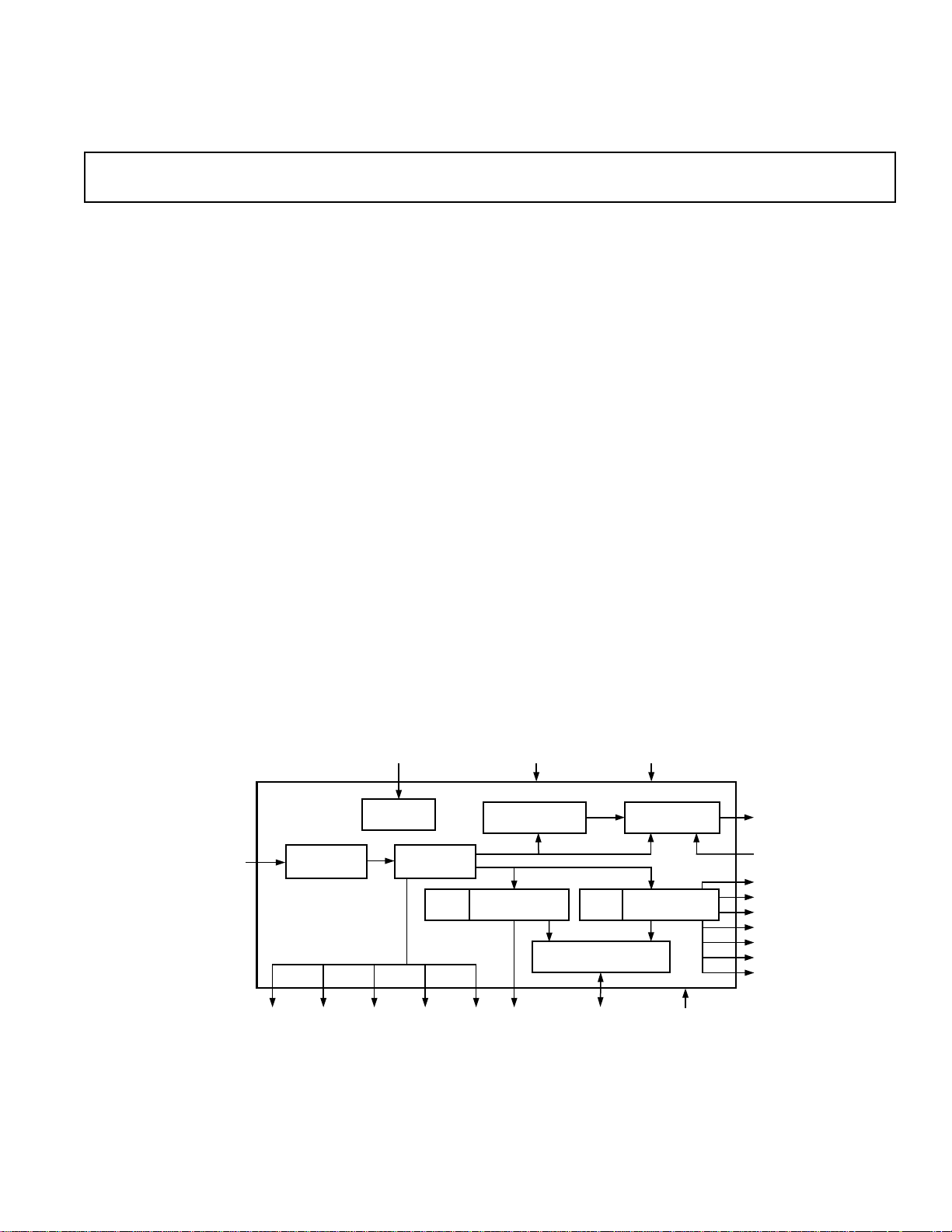
PRODUCT OVERVIEW
The AD1892 combines a CP-1201, CP-340, IEC-958, AES/
EBU, S/PDIF compatible Digital Audio Receiver (DAR) with
an asynchronous sample rate converter, allowing the user to
specify the output sample rate of the received digital audio information. The DAR block features support for both Q-channel
subcode information (to support CD, CD-R, MD and DAT
digital audio formats) as well as Channel Status information. A
microcontroller interface, with an SPI compatible serial port,
allows full access to the 80-bit Q-Channel subcode buffer and to
the 32-bit Channel Status buffer, as well as to the control and
status registers. Additionally, key status information from the
incoming subframes and the Channel Status buffer is reported
on status output pins on the AD1892, so the AD1892 may be
used in systems that do not include a microcontroller or
microprocessor.
The asynchronous sample rate converter block is based on
market leading AD1890 family SamplePort
nology. The AD1892 offers a 1:5 upsampling range, and will
downsample from 48 kHz to 44.1 kHz. Input audio word widths
up to 20 bits are supported, and output audio word widths of 16
or 20 are supported, with 120 dB of dynamic range and –113 dB
THD+N. The rate converter inherently rejects jitter on the
recovered clocks from the incoming biphase-mark encoded
stream. Indeed, sample rate conversion is highly synergistic
with digital audio reception, allowing the use of a fully digital
phase locked loop clock recovery scheme with highly robust
clock recovery and jitter rejection.
rate conversion tech-
(continued on Page 4)
FUNCTIONAL BLOCK DIAGRAM
512 x F
SOUT
CLOCK
GENERATOR
INPUT
2
SIGNAL
BIPHASE-MARK
NO
RECEIVER
AD1892
ERROR
INTERRUPT
COMPARATOR
CRC
CHECK
U/C BIT SFCLK
BIPHASE-MARK
SamplePort is a registered trademark of Analog Devices, Inc.
SPI is a trademark of Motorola, Inc.
REV. 0
Information furnished by Analog Devices is believed to be accurate and
reliable. However, no responsibility is assumed by Analog Devices for its
use, nor for any infringements of patents or other rights of third parties
which may result from its use. No license is granted by implication or
otherwise under any patent or patent rights of Analog Devices.
POWER-DOWN/RESET
ASYNCH SAMPLE
RATE CONVERTER
DATA
CONTROL
Q-CHANNEL
SUBCODE BUFFER
QDFS
One Technology Way, P.O. Box 9106, Norwood, MA 02062-9106, U.S.A.
Tel: 781/329-4700 World Wide Web Site: http://www.analog.com
Fax: 781/326-8703 © Analog Devices, Inc., 1998
CRC
CHECK
MICROCONTROLLER
INTERFACE
CLOCK, LATCH,
DATA IN,
DATA OUT
MUTE
BCLK
OUTPUT SERIAL
INTERFACE
BYPASS
CHANNEL STATUS
BUFFER
42
DIGITAL
SUPPLY
3
LRCLK
SDATA
SYNC
CA
CB
CC
CD
CE
CON/PRO
CSCLK
Page 2

AD1892–SPECIFICATIONS
TEST CONDITIONS UNLESS OTHERWISE NOTED
Supply Voltage +5.0 V
Ambient Temperature 25 °C
Output Sample Frequency (F
MCLK 25 MHz (512 × F
Input Word Width 20 Bits
Load Capacitance 100 pF
All minimums and maximums tested except as noted.
) 48.8 kHz
SOUT
SOUT
)
PERFORMANCE
1
Min Typ Max Units
Dynamic Range (20 Hz to 20 kHz, –60 dB Input) 120 dB
Total Harmonic Distortion + Noise
(20 Hz to 20 kHz, Full-Scale Input) –103 dB
(1 kHz Full-Scale Input) –113 dB
(10 kHz Full-Scale Input) –107 dB
Interchannel Phase Deviation 0 Degrees
DIGITAL I/O
1
Min Typ Max Units
V
IH
V
IL
@ V
I
IH
I
IL
V
OH
V
OL
Input Capacitance
DIGITAL TIMING
= +5.0 V 10 µA
IH
@ V
= 0 V 10 µA
IL
@ IOH = –0.5 mA DVDD – (0.5) V
@ IOL = 0.5 mA 0.5 V
1
1
2.4 V
0.8 V
15 pF
Min Typ Max Units
t
MCP
F
MCLK
t
PDRP
t
BDM
t
LDM
t
DDP
t
DDS
t
DDH
t
SSU
t
CCH
t
CCL
t
CCP
t
CSU
t
CHD
t
COH
t
SFPW
t
SFSU
t
CSPW
t
QDH
t
CLH
t
CLK
t
RS
MCLK Duty Cycle
MCLK Frequency (1/t
PD/RST LO Pulsewidth 10 × MCLK Period ns
BCLK Propagation Delay from MCLK (to Falling Edge) 30 ns
LRCLK Propagation Delay from MCLK 30 ns
Data Propagation Delay from MCLK 30 ns
Data Output Setup to BCLK 1/2 BCLK Period ns
Data Output Hold from BCLK 1/2 BCLK Period ns
SYNC Falling Setup to MCLK Rising 5 ns
CCLK HI Pulsewidth 20 ns
CCLK LO Pulsewidth 20 ns
CCLK Period 8 × MCLK Period ns
SDI Setup 15 ns
SDI Hold 10 ns
SDO Propagation Delay from CCLK 30 ns
SFCLK HI Pulsewidth
U/CBIT, INT, ERROR Setup to SFCLK 100 ns
CSCLK HI Pulsewidth
QDFS HI Pulsewidth
CS HI Pulsewidth 10 × MCLK Period ns
CS Falling Edge to CCLK Rising 3 × MCLK Period ns
PD/RST Rising to MCLK Rising Edge (Only Required
1
1
)
MCP
1
1
1
40 60 %
25 MHz
100 ns
100 ns
1000 ns
for Synchronizing Multiple Parts) 5 ns
DIGITAL RS-422 RECEIVERS (RXP, RXN Pins Only)
Min Typ Max Units
Input Resistance 20 kΩ
Min Differential AES/EBU or S/PDIF Input 200 mV p-p
Input Hysteresis 20 mV
REV. 0–2–
Page 3
POWER
WARNING!
ESD SENSITIVE DEVICE
Min Typ Max Units
Supplies
Voltage, DV
DD
Operational Current, I
Power-Down Current, I
Dissipation
1
(DVDD = +5.0 V) 50 60 mA
DD
(DVDD = +5.0 V) (PD/RST LO) 3 6 mA
DD
4.5 5.5 V
Operational (DVDD = +5.0 V) 250 300 mW
Power-Down (DVDD = +5.0 V) (PD/RST LO) 15 30 mW
TEMPERATURE RANGE
Min Max Units
Specifications Guaranteed –40 +85 °C
Storage –55 +125 °C
AD1892
ABSOLUTE MAXIMUM RATINGS
2
Min Max Units
DV
to DGND –0.3 7.0 V
DD
DC Input Voltage –0.3 DV
+ 0.3 V
DD
Soldering +300 °C
10 sec
DIGITAL FILTER CHARACTERISTICS
1
Min Max Units
Passband Ripple (0 kHz to 20 kHz) (F
= 44.1 kHz) ±0.015 dB
S
Group Delay (LRCLK = 50 kHz) 700 3000 µs
NOTES
1
Guaranteed, not tested.
2
Stresses greater than those listed under Absolute Maximum Ratings may cause permanent damage to the device. This is a stress rating only; functional operation of
the device at these or any other conditions above those indicated in the operational section of this specification is not implied. Exposure to absolute maximum rating
conditions for extended periods may affect device reliability.
Specifications subject to change without notice.
ORDERING GUIDE
Model Temperature Range Package Description Package Options
AD1892JR –40°C to +85°C 28-Lead SOIC R-28
AD1892JRRL –40°C to +85°C 28-Lead SOIC R-28 on 13" Reels
CAUTION
ESD (electrostatic discharge) sensitive device. Electrostatic charges as high as 4000 V readily
accumulate on the human body and test equipment and can discharge without detection.
Although the AD1892 features proprietary ESD protection circuitry, permanent damage may
occur on devices subjected to high energy electrostatic discharges. Therefore, proper ESD
precautions are recommended to avoid performance degradation or loss of functionality.
REV. 0
–3–
Page 4

AD1892
(continued from Page 1)
PRODUCT OVERVIEW (Continued)
In addition to the Q-channel subcode and Channel Status buffers, the AD1892 includes two 8-bit control registers and two 8bit status registers. The output data interface may be configured
in left-justified, I
2
S-justified and right-justified modes. The
AD1892 includes hardware power-down/reset and mute control
inputs, and power-down/reset and mute may also be invoked
through write to bits in the control registers. The AD1892
operates from a master clock that must be synchronous with the
output sample rate at 512 × F
. Cyclic Redundancy Coding
S
(CRC) error detection is performed over the full 80 bits of the
received Q-channel subcode information in consumer mode, as
well as the full 192 bits of the received Channel Status information in professional mode.
The AD1892 includes a SYNC input (Pin 23) that allows
multiple AD1892s in a system to be synchronized to a common
LEFT/RIGHT clock.
The AD1892 is offered in a 28-lead SOIC package. It operates
over the industrial temperature range from –40°C to +85°C
at a supply voltage from 4.5 V to 5.5 V. The only external
components required to support the AD1892 are power supply
decoupling capacitors.
DEFINITIONS
Dynamic Range
The ratio of a full-scale input signal to the integrated noise in the
passband (0 kHz to ≈20 kHz), expressed in decibels (dB).
Dynamic range is measured with a –60 dB input signal and
“60 dB” arithmetically added to the result. This measurement
technique is consistent with the recommendations of the Audio
Engineering Society (AES17-1991) and the Electronic Industries
Association of Japan (EIAJ CP-307).
Total Harmonic Distortion + Noise
Total Harmonic Distortion plus Noise (THD+N) is defined as
the ratio of the square root of the sum of the squares of the
values of the harmonics and noise to the value of the fundamental input frequency. It is usually expressed in percent (%) or
decibels.
Interchannel Phase Deviation
Difference in input sampling times between stereo channels,
expressed as a phase difference in degrees between 1 kHz inputs.
Group Delay
The time interval required for the frequency components of an
input pulse to appear at the converter’s output, expressed in
milliseconds (ms). More precisely, the derivative of radian phase
with respect to radian frequency at a given frequency.
AD1892 PIN LIST
Biphase-Mark Serial Input
Pin Name SOIC I/O Description
RXP 13 I Positive differential biphase-mark serial digital audio receiver input. 20 mV hysteresis.
RXN 14 I Negative differential biphase-mark serial digital audio receiver input. 20 mV hysteresis.
Serial Output Interface
Pin Name SOIC I/O Description
SDATA 24 O Serial output, MSB first, containing two channels of 16 to 20 bits (default) of twos-complement
data per channel, depending on control register settings. The data can be configured in I
2
S-justified
(default), left-justified, and right-justified orientations, depending on control register settings. See
Figure 36 for timing.
BCLK 26 O Bit clock output for output data. Frequency is either 32 × F
(packed mode) or 64 × F
S
(default),
S
depending on control register settings. See Figure 36 for timing.
LRCLK 25 O LEFT/RIGHT clock output for output data. Runs continuously and is a synchronous divide-down
from MCLK (MCLK/512). See Figure 36 for timing.
SYNC 23 I The SYNC input allows multiple AD1892s in a system to be phase and group delay synchronized to
the same LEFT/RIGHT clock. The SYNC signal resets internal AD1892 counters such that 512 MCLK
cycles after the falling edge of SYNC, the AD1892 data will be valid, and the AD1892 LRCLK signal
will change state. It is recommended that the SYNC input be used only when the AD1892 is in the
64 × F
Decoded Channel Status Outputs
BCLK mode (default configuration). GND when not in use.
SOUT
Pin Name SOIC I/O Description
CA 21 O In consumer or professional mode, CA is the inverse of Channel Status Bit 1, Byte 0 (C1, audio/
nonaudio). CA = 0 indicates nonaudio, CA = 1 indicates audio. CA = 0 can be used to indicate
Dolby AC-3 encoded data.
CB 20 O In consumer mode, CB is the inverse of Channel Status Bit 2, Byte 0 (C2, copy/copyright). CB = 0
indicates copy permitted/copyright not asserted; CB = 1 indicates copy inhibited/copyright asserted.
In professional mode, CB is defined as EM0, the least significant bit of the two bits that encodes the
emphasis status of the audio material.
–4–
REV. 0
Page 5

AD1892
Decoded Channel Status Outputs (Continued)
Pin Name SOIC I/O Description
CC 19 O In consumer mode, CC is the inverse Channel Status Bit 3, Byte 0 (C3, pre-emphasis). CC = 0
indicates that the audio material has been pre-emphasized; CC = 1 indicates that the audio material
has not been pre-emphasized.
In professional mode, CC is the most significant bit of the two bits that encodes the emphasis status
of the audio material.
Table I illustrates the professional mode emphasis encoding.
Table I. Professional Mode Emphasis Encoding
AD1892 BYTE 0
Output Channel Status Bit
CC CB C2 C3 C4 Status
1 1 0 0 0 Emphasis not indicated. Receiver defaults to
no emphasis with manual override enabled.
1 0 1 0 0 None. Receiver manual override disabled.
0 1 1 1 0 50/15 µs. Receiver manual override disabled.
0 0 1 1 1 CCITT J. 17. Receiver manual override disabled.
CD 18 O In consumer mode, CD indicates that the audio material is original over all category codes. The
state of this bit is affected by both the generation status “L” bit (Channel Status Bit 15, Byte 1) and
the category code (Channel Status Bits 8 through 14, Byte 1) since the definition of the L bit is reversed for three of the category codes (001XXXX, 0111XXX, and 100XXXX). CD = 0 indicates
that the audio material is original. CD = 1 indicates that the audio material is a copy (first generation or higher).
In professional mode, CD is the inverse of Channel Status Bit 9, Byte 1. CD provides some information about channel mode. See below for additional details.
CE 17 O In consumer mode, CE indicates the so-called “ignorant” category codes of “general” (0000 000)
and “A/D converter without copyright information” (0110 000). CE = 1 indicates that the audio
material is not encoded using an ignorant category code. CE = 0 indicates that the audio material is
encoded using an ignorant category code. This status output can be used in conjunction with the
CD output (Pin 18) to implement SCMS copy protection. See below for additional details.
In professional mode, CE indicates a Cyclic Redundancy Code (CRC) check error. CE = 0 indicates that the calculated CRC value does not match the received CRC value. CE = 1 indicates that
the calculated CRC value does match the received CRC value. CE may be used to enable the display of the CA through CD states. If CE = 0, then CA through CD may be considered to be in
error, and their display should not be updated.
The Table II summarizes the function of the CA through CE pins, depending on the operating mode
(professional or consumer).
Table II. Decoded Channel Status Output Functions
Pin Consumer Professional
CA 0 = Audio, 1 = Nonaudio 0 = Audio, 1 = Nonaudio
CB 0 = Copy Permitted, 1 = Copy Inhibited Pre-emphasis Encoding
CC 0 = Pre-emphasis, 1 = No Pre-emphasis Pre-emphasis Encoding
CD 0 = Original, 1 = Copy Inverse of Channel Status Bit 9
CE 0 = Ignorant Category, 1 = Not Ignorant 0 = C.S. CRC Error, 1 = No C.S. CRC Error
PRO 15 O CON/PRO is defined as the inverse Channel Status bit 0, byte 0 (C0, pro/consumer). CON/PRO =
CON/
0 indicates professional mode. CON/PRO = 1 indicates consumer mode. The state of this pin internally determines the consumer/pro mode of the CA, CB, CC, CD and CE pins.
CSCLK 16 O Channel Status Clock. Active HI (rising edge active). Outputs a pulse every 192 frames at the
start of the Channel Status block. Use the falling edge of this clock to latch the CA through CE
and CON/PRO output Channel Status signals. See Figure 38 for timing.
REV. 0 –5–
Page 6

AD1892
Subframe Status Outputs
Pin Name SOIC I/O Description
NOSIG 12 O NOSIG (No Signal) is asserted HI when no biphase-mark input is applied to the AD1892 when
either the input sample rate is too high for the applied master clock (MCLK) frequency or, equivalently, the master clock frequency is too low for the applied input sample rate. NOSIG is deasserted
LO during normal operation. This signal is asynchronous and has no particular timing relationship
with any of the clock signals associated with the AD1892.
ERROR 11 O The ERROR pin is asserted HI when either a subframe parity error or a subframe validity error
occurs. Logically, ERROR = PARITY ERROR or VALIDITY ERROR. The ERROR pin is deasserted LO when neither parity nor validity errors are detected. The state of this output pin is not
directly reflected in the AD1892 status registers; rather, Status Register 0 has separate bits that
indicate parity and validity errors. The ERROR output should be clocked using the SFCLK signal
(Pin 8). The ERROR output signal is NOT sticky, so it can be used in applications that do not include a supporting microcontroller.
INT 10 O INT (Interrupt) is asserted HI when any of the first 32 bits of Channel Status information changes
from block to block or when the Q-Channel subcode track number (Q10 through Q17) changes
from block to block (valid in consumer mode only). The Channel Status block spans 192 frames (or
subframes, since either the left or right channel C bit is stored), and the Q-Channel subcode block
spans 1176 subframes. INT is deasserted LO when neither the first 32 bits of Channel Status
changes from block to block when the Q-Channel subcode track number changes from block to
block. This output is mirrored in a status bit (Status Register 0, Bit 5). The INT output can be
clocked using the SFCLK signal (Pin 8). The INT output signal is sticky and can only be cleared by
reading Status Register 0.
U/CBIT 9 O U/CBIT is either the subframe user bit or the Channel Status bit from the biphase-mark stream, fed
out serially, valid on the rising edge of the SFCLK signal (Pin 8). The choice between user bit and
Channel Status bit is determined by Bit 1 in Control Register 0 (0 user bit [default], 1 = Channel
Status bit). Changes at the subframe rate (two times the incoming sample rate.) See Figure 39 for
timing.
SFCLK 8 O This SFCLK signal is used to clock the ERROR, INT and U/CBIT output status signals. Active
LO (rising edge active); see Figure 39 for timing. It is a LO pulse at the subframe rate (two times
the sample rate). The pulsewidth is approximately 1/64th of the incoming sample (frame) period.
Q-Channel Subcode Clock Output Signal
Pin Name SOIC I/O Description
QDFS 6 O QDFS (Q-Channel Data Frame Sync) is a framing pulse indicating if the AD1892 has finished col-
lecting a full Q-Channel subcode block of user bits, which has a period of 1176 subframes. Can be
used as an interrupt signal to a microcontroller. The QDFS output is HI for one subframe period.
The QDFS frequency is 75 Hz when the incoming input sample rate is 44.1 kHz. See Figure 40 for
timing information.
Serial Control Port Signals
Pin Name SOIC I/O Description
CS 3 I Chip Select/Latch signal for the serial control port. This input must be LO for any write or read
operation using the serial control port to be valid. This input should be tied HI when using the
AD1892 in a stand-alone (no external microcontroller) application. See the Serial Control Port
Timing in Figure 37 and the text below for more information.
CCLK 2 I Serial Control Port Clock. This rising edge active input samples the address and data associated
with the serial control port. The frequency of CCLK signal must not exceed 1/8 the frequency of
the MCLK (Pin 28) signal. See the Serial Control Port Timing in Figure 37 and the text below for
more information.
SDI 4 I Serial Data Input. This input signal is used to convey the serial 6-bit address, the read/write indication
and the 8-bit write data for the AD1892 serial control port. See the Serial Control Port Timing in
Figure 37 and the text below for more information.
SDO 5 O Serial Data Output. This three-state output is used to convey the serial 8-bit read data for the
AD1892 serial control port. It is a three-state output to allow multiple AD1892s to coexist on the same
SPI serial bus. See the Serial Control Port Timing in Figure 37 and the text below for more information.
–6–
REV. 0
Page 7
AD1892
Power Supply Connections
Pin Name SOIC I/O Description
DV
DD
DGND 7 Digital Ground. +0 V nominal supply connection.
Miscellaneous
Pin Name SOIC I/O Description
MCLK 28 I Master clock. Must be 512 × F
PD/RST 1 I Active LO power-down/reset, which clears all on-chip registers on the AD1892 to their default state
MUTE 27 I Mute input. HI hardware mutes the serial digital audio output to zeros (midscale). All control
22 Digital Supply. +5 V nominal supply voltage.
, where F
SOUT
SOUT
and stops the on-chip clocks. Bring HI for normal chip operation.
functions on the AD1892 (Channel Status, Q-Channel subcode, etc.) continue to function while the
AD1892 is muted. Should be LO for normal operation.
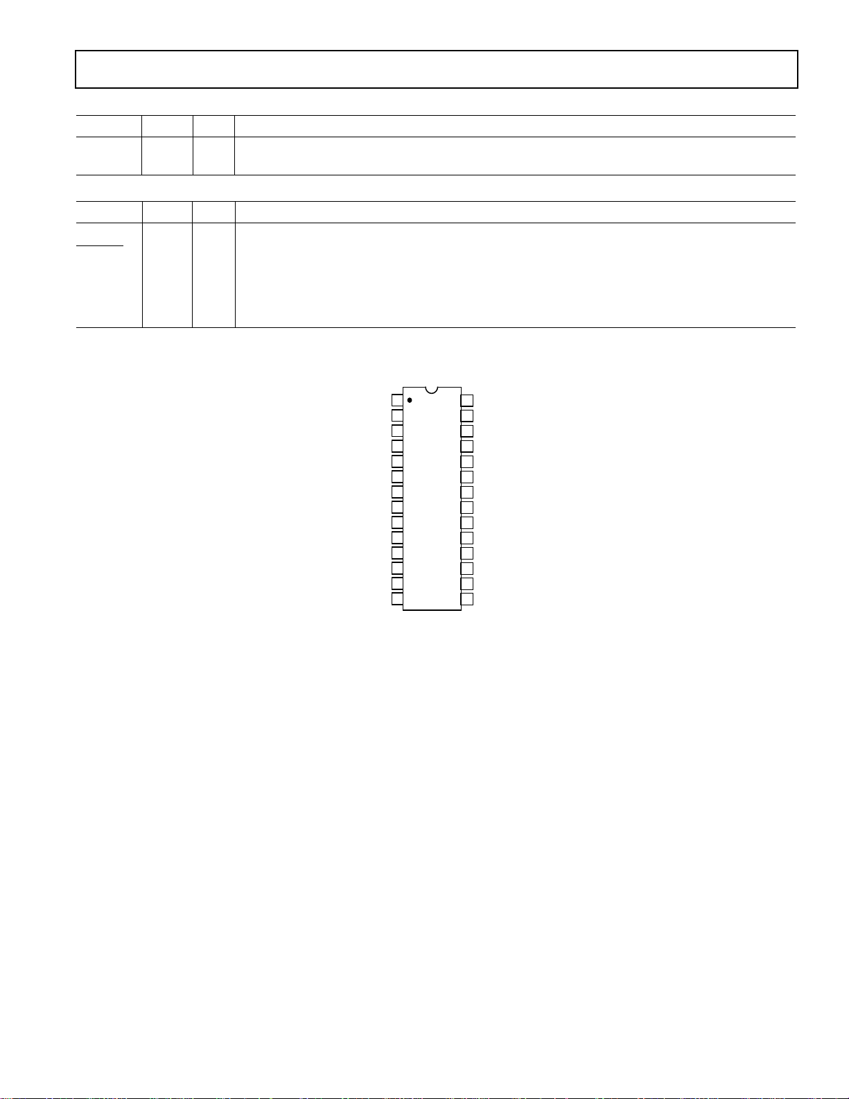
PIN CONFIGURATION
is the desired output sample rate.
PD/RST
CCLK
CS
SDI
SDO
QDFS
DGND
SFCLK
U/CBIT
INT
ERROR
NOSIG
RXP
RXN
1
2
3
4
5
6
TOP VIEW
(Not to Scale)
7
8
9
10
11
12
13
14
AD1892
MCLK
28
MUTE
27
26
BCLK
25
LRCLK
24
SDATA
23
SYNC
22
DV
21
CA
20
CB
19
CC
18
CD
17
CE
16
CSCLK
15
CON/PRO
DD
REV. 0 –7–
Page 8
AD1892
PREAMBLES
X LEFT CH Y RIGHT CH Z LEFT CH Y RIGHT CH X LEFT CH Y RIGHT CH X
FRAME 191
FRAME 0
FRAME 1
START OF CHANNEL STATUS BLOCK
SUB-
FRAME
SUB-
FRAME
PREAMBLE X
PREAMBLE Y
PREAMBLE Z
11011000
11001010
11101000
SERIAL DIGITAL AUDIO TRANSMISSION STANDARDS
The AD1892 can receive S/PDIF (Sony/Philips Digital Interface
Format), AES/EBU (Audio Engineering Society/European
Broadcasting Union, also known as AES3-1992), IEC-958
(International Electrotechnical Commission) and CP-340 (EIAJ
[Electronic Industry Association of Japan] CP-1201) serial
streams. S/PDIF is a consumer audio standard, and AES/EBU
is a professional audio standard; IEC-958 and CP-340 have
both consumer and professional definitions. This data sheet is
not intended to fully define or to provide a tutorial for these
standards; please contact these international standards setting
bodies for the full specifications.
All of these digital audio serial communication schemes encode
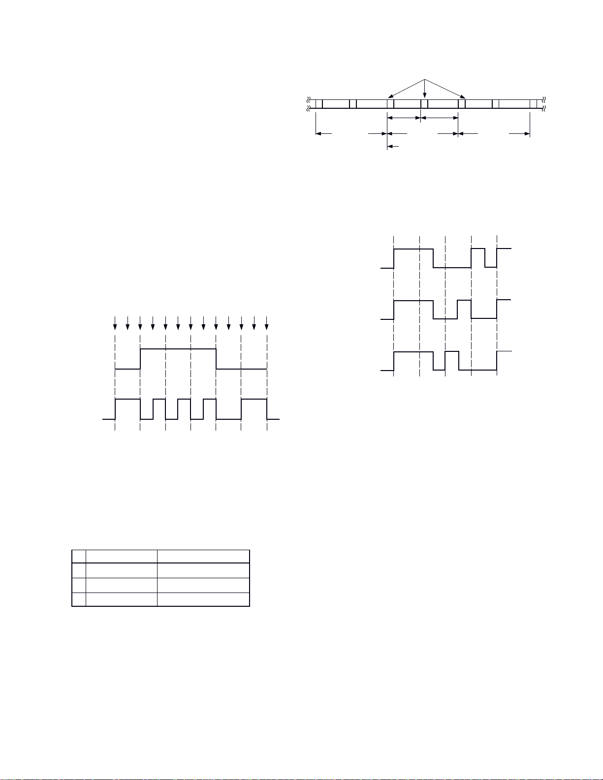
audio data and audio control information using the biphasemark method. This encoding method minimizes the dc content
of the transmitted signal and allows the receiver to decode clock
information from the transmitted signal. As can be seen from
Figure 1, ones in the original data end up with midcell transitions in the biphase-mark encoded data, while zeros in the original data do not. Note that the biphase-mark encoded data
always has a transition between bit boundaries.
Figure 3. Preambles, Frames and Subframes
The biphase-mark encoding violations are shown in Figure 4.
Note that all three preambles include encoding violations. Ordinarily, the biphase-mark encoding method results in a polarity
transition between bit boundaries.
(2 TIMES BIT RATE)
CLOCK
DATA
BIPHASE-MARK
DATA
011100
1
01001010111
Figure 1. Biphase-Mark Encoding
Digital audio communication schemes use “preambles” to distinguish between channels (called “subframes”) and between
longer term control information blocks (called “frames”). Preambles are particular biphase-mark patterns, which contain
encoding violations that allow the receiver to uniquely recognize
them. These patterns, and their relationship to frames and
subframes, are shown in Figures 2 and 3.
BIPHASE PATTERNS
11100010 OR 00011101
X
11100100 OR 00011011
Y
11101000 OR 00010111
Z
CHANNEL
LEFT
RIGHT
LEFT AND C.S. BLOCK START
Figure 4. Preambles
As noted above, these serial digital audio communication
schemes are organized using a frame and subframe construction.
There are two subframes per frame (ordinarily the left and right
channel). Each subframe includes the appropriate four bit
preamble, four bits of “auxiliary” (aux) data, 20 bits of audio
data (LSB first), a “validity” (V) bit, a “user” (U) data bit, a
Channel Status (C) bit and an even parity (P) bit. The Channel
Status bits and the user bits accumulate over many frames to
convey control information. The Channel Status bits accumulate over a 192 frame period (called a Channel Status block).
The user bits accumulate over 1176 frames when the interconnect is implementing the so-called “subcode” scheme
(EIAJ CP-2401). The organization of the Channel Status
block, frames and subframes is shown in Figure 5.
Figure 2. Biphase-Mark Encoded Preambles
–8–
REV. 0
Page 9

AD1892
7
EMPHASIS
LOCK
F
S
AUDIO
PRO = 1BYTE 0
1
2
3
4
5
6
7
8
9
10
11
12
13
14
15
16
17
18
19
20
21
22
23
7
15
23
31
39
47
55
87
119
151
183
191
BLOCK
BIT
654321BIT 0
CHANNEL MODE USER BIT MANAGEMENT
RESERVEDWORD LENGTHAUX USE
RESERVED
RESERVED
REFERENCE
RESERVED
ALPHANUMERIC CHANNEL ORIGIN DATA
ALPHANUMERIC CHANNEL DESTINATION DATA
LOCAL SAMPLE ADDRESS CODE
(32-BIT BINARY)
TIME OF DAY CODE
(32-BIT BINARY)
RESERVED RELIABILITY FLAGS
CYCLIC REDUNDANCY CHECK CHARACTER
CHANNEL STATUS BLOCK (384 AUDIO SAMPLES)
A0 B0 A1 B1 A2 B2 A3 B3 A4 B4 A5 B5 A6 B6 A7 B7 A8 B8
192 LEFT, 192 RIGHT
(EXPANDED)
FRAME
A0 B0 A1 B1 A2 B2
(EXPANDED)
87430
LSBAUX DATAPREAMBLE
SUBFRAME
AUDIO DATA V U C P
Figure 5. Block, Frame and Subframe Organization
A188 B188 A189 B189 A190 B190 A191 B191
A = LEFT CHANNEL
B = RIGHT CHANNEL
27 28 29 30 31
MSB
VALIDITY
USER DATA
CHANNEL STATUS DATA
EVEN PARITY BIT
As noted above, the Channel Status bit from each subframe
accumulates over a 192 subframe period. The standards allow for
the Channel Status bit in each subframe to be independent, but
ordinarily the Channel Status bit in the two subframes of each
frame are the same. The Channel Status bits are defined
7
654321BIT 0
AUDIO
PRO = 0BYTE 0
1
2
3
4
5
6
7
8
9
10
11
12
13
14
15
16
17
18
19
20
21
22
23
SOURCE NUMBER
CATEGORY CODE
F
S
RESERVED
EMPHASIS
CHANNEL NUMBER
CLOCK ACCURACY
RESERVED
MODECOPY
L
Figure 6. Consumer Channel Status Block Structure
REV. 0 –9–
BLOCK
BIT
7
15
23
31
39
191
differently for the consumer audio standards and the professional audio standards. The 192 Channel Status bits are
organized into 24 bytes and have the interpretations shown in
Figures 6 through 16.
Figure 7. Professional Channel Status Block Structure
Page 10

AD1892
BYTE 1
BITS 0 1 2 3 4 5 6 CATEGORY CODE
GENERAL. "IGNORANT" CATEGORY CODE.
EXPERIMENTAL.
RESERVED.
SOLID STATE MEMORY.
BROADCAST RECEPTION OF DIGITAL AUDIO.
L BIT DEFINITION REVERSED.
JAPAN
UNITED STATES.
EUROPE.
ELECTRONIC SOFTWARE DELIVERY.
ALL OTHER STATES ARE RESERVED.
DIGITAL/DIGITAL CONVERTERS
PCM ENCODER/DECODER.
DIGITAL SOUND SAMPLER.
DIGITAL SIGNAL MIXER.
SAMPLE RATE CONVERTER.
ALL OTHER STATES ARE RESERVED.
A/D CONVERTERS
A/D CONVERTER W/O COPY PROTECTION INFO
"IGNORANT" CATEGORY CODE.
A/D CONVERTER W/COPY PROTECTION INFO
(USING COPY AND L BITS).
BROADCAST RECEPTION OF DIGITAL AUDIO.
L BIT DEFINITION REVERSED.
LASER OPTICAL. L BIT DEFINITION REVERSED.
CD – COMPATIBLE WITH IEC-908.
CD – NOT COMPATIBLE WITH IEC-908.
(MAGNETO-OPTICAL).
MD – MINIDISC.
ALL OTHER STATES ARE RESERVED.
MUSICAL INSTRUMENTS, MICS, ETC.
SYNTHESIZER.
MICROPHONE.
ALL OTHER STATES ARE RESERVED.
MAGNETIC TAPE OR DISK
DAT – DIGITAL AUDIO TAPE.
VIDEO TAPE RECORDER WITH DIGITAL AUDIO.
DCC – DIGITAL COMPACT CASSETTE
ALL OTHER STATES ARE RESERVED.
RESERVED
BIT 7 L: GENERATION STATUS
ONLY CATEGORY CODES: 1 0 0 X X X X,
0 0 1 X X X X, 0 1 1 1 X X X
ORIGINAL/COMMERCIALLY PRE-RECORDED DATA.
NO INDICATION /1ST GENERATION OR HIGHER.
ALL OTHER CATEGORY CODES
NO INDICATION /1ST GENERATION OR HIGHER.
ORIGINAL/COMMERCIALLY PRERECORDED DATA.
0 0 0 0 0 0 0
0 0 1
X X X
X X X
0 0 1
0 0 0 0
0 0 1 1
1 0 0 0
0 0 0 1
0 1 0
0 0 0 0
0 0 1 0
0 1 0 0
1 1 0 0
X X X X
0 1 1 0
0 0 0
1 0 0
1 0 0
0 0 0 0
1 0 0 0
1 0 0 1
X X X X
1 0 1
0 0 0 0
1 0 0 0
X X X X
1 1 0
0 0 0 0
1 0 0 0
X X X X
0 0 0 1
0
1
0
1
0 0 0 1
X X X X
X X X
0 1 1 1
1 1 1
X X X X
BIT 0
0
1
BIT 1
0
1
BIT 2
0
1
BITS 3 4 5
0 0 0
1 0 0
0 1 0
1 1 0
X X 1
BITS 3 4 5
0 0 0
X X X
BITS 6 7
0 0
X X
Figure 8. Consumer Channel Status Byte 0
PRO = 0 (CONSUMER)
CONSUMER USE OF CHANNEL STATUS BLOCK.
PROFESSIONAL USE OF CHANNEL STATUS BLOCK.
AUDIO
DIGITAL AUDIO.
NON-AUDIO. CAN BE USED TO INDICATE AC-3 DATA.
COPY/COPYRIGHT.
COPY INHIBITED/COPYRIGHT ASSERTED.
COPY PERMITTED/COPYRIGHT NOT ASSERTED.
PRE-EMPHASIS – IF BIT 1 = 0 (DIGITAL AUDIO)
NONE – 2 CHANNEL AUDIO.
50/15 µs – 2 CHANNEL AUDIO.
RESERVED – 2 CHANNEL AUDIO.
RESERVED – 2 CHANNEL AUDIO.
RESERVED – 4 CHANNEL AUDIO.
IF BIT 1 = 1 (NON-AUDIO)
DIGITAL DATA.
ALL OTHER STATES OF BITS 3–5 ARE RESERVED.
MODE
MODE 0 (DEFINES BYTES 1–3)
ALL OTHER STATES OF BITS 6–7 ARE RESERVED.
BYTE 0
–10–
Figure 9. Consumer Channel Status Byte 1
REV. 0
Page 11

48 kHz. MANUAL OVERRIDE OR AUTO SET DISABLED.
SAMPLE FREQUENCY NOT INDICATED.
RECEIVER DEFAULTS TO 48 kHz AND MANUAL
OVERRIDE OR AUTO SET ENABLED.
FS: SAMPLE FREQUENCY
UNLOCKED.
LOCKED–DEFAULT.
LOCK: SOURCE SAMPLE FREQUENCY
ALL OTHER STATES OF BITS 2–4 ARE RESERVED.
CCITT J.17. RECEIVER MANUAL OVERRIDE DISABLED.
50/15 µs. RECEIVER MANUAL OVERRIDE DISABLED.
NONE. RECEIVER MANUAL OVERRIDE DISABLED.
EMPHASIS NOT INDICATED. RECEIVER DEFAULTS
TO NO EMPHASIS WITH MANUAL OVERRIDE ENABLED.
ENCODED AUDIO SIGNAL EMPHASIS
NON-AUDIO. CAN BE USED TO INDICATE AC-3 DATA.
NORMAL AUDIO.
AUDIO
PROFESSIONAL USE OF CHANNEL STATUS BLOCK.
CONSUMER USE OF CHANNEL STATUS BLOCK.
PRO = 1 (PROFESSIONAL)
BYTE 0
BIT 0
0
1
0
BIT 1
1
BITS 2 3 4
0 0 0
1 1 0
1 0 0
X X X
0
1
BITS 6 7
0 0
0 1
BIT 5
1 1 0
44.1 kHz. MANUAL OVERRIDE OR AUTO SET DISABLED.1 0
32 kHz. MANUAL OVERRIDE OR AUTO SET DISABLED.
1 1
BYTE 1
BITS 0 1 2 3 CHANNEL MODE
MODE NOT INDICATED. RECEIVER DEFAULTS TO
2-CHANNEL MODE. MANUAL OVERRIDE ENABLED.
0 0 0 0
0 0 0 1
0 0 1 0
0 0 1 1
0 1 0 0
TWO CHANNELS. MANUAL OVERRIDE DISABLED.
SINGLE CHANNEL. MANUAL OVERRIDE DISABLED.
PRIMARY/SECONDARY (CH. A IS PRIMARY). MANUAL
OVERRIDE DISABLED.
STEREOPHONIC (CH. A IS LEFT). MANUAL OVERRIDE
DISABLED.
0 1 0 1
0 1 1 0
BITS 4 5 6 7 USER BIT MANAGEMENT
0 0 0 0
0 0 0 1
0 0 1 0
0 0 1 1
DEFAULT. NO USER INFORMATION INDICATED.
192 BIT BLOCK STRUCTURE. PREAMBLE 'Z' STARTS
BLOCK.
RESERVED.
ALL OTHER STATES OF BITS 4–7 ARE RESERVED.
RESERVED FOR USED DEFINED APPLICATIONS.
VECTOR TO BYTE 3. RESERVED.
1 1 1 1
RESERVED FOR USED DEFINED APPLICATIONS.
ALL OTHER STATES OF BITS 0–3 ARE RESERVED.
X X X X
USER DEFINED APPLICATION.
X X X X
BYTE 2
BITS 0 1 2 3 SOURCE NUMBER
UNSPECIFIED.0 0 0 0
1 0 0 0
0 1 0 0
1 1 0 0
0 0 1 0
0 1 1 1
1 1 1 1
BITS 4 5 6 7 CHANNEL NUMBER
1 0 0 0
0 1 0 0
1 1 0 0
0 1 1 1
Figure 10. Consumer Channel Status Byte 2
BITS 0 1 2 3 FS: SAMPLE FREQUENCY
0 1 0 0
1 1 0 0
X X X X
BITS 4 5 CLOCK ACCURACY
0 1
1 0
1 1
BITS 6 7
RESERVED
1
2
3
4 TO
14 (BINARY – BIT 0 IS LSB, BIT 3 IS MSB)
15
UNSPECIFIED.0 0 0 0
A (LEFT IN 2 CHANNEL FORMAT)
B (RIGHT IN 2 CHANNEL FORMAT)
C TO
N (BINARY – BIT 4 IS LSB, BIT 7 IS MSB)
O1 1 1 1
BYTE 3
44.1 kHz.0 0 0 0
48 kHz.
32 kHz.
ALL OTHER STATES OF BITS 0–3 ARE RESERVED.
LEVEL II, 61000 ppm (DEFAULT).0 0
LEVEL III, VARIABLE PITCH.
LEVEL I, 650 ppm – HIGH ACCURACY.
RESERVED.
RESERVED.X X
BYTES 4–23
AD1892
Figure 11. Consumer Channel Status Bytes 3 Through 23
REV. 0 –11–
Figure 12. Professional Channel Status Bytes 0 and 1
Page 12

AD1892
BYTES 6–9
ALPHANUMERIC CHANNEL ORIGIN DATA.
7-BIT ISO 646 (ASCII) DATA WITH ODD PARITY BIT. FIRST CHARACTER IN
MESSAGE IS BYTE 6. LSBs ARE TRANSMITTED FIRST.
BYTES 10–13
ALPHANUMERIC CHANNEL ORIGIN DATA.
7-BIT ISO 646 (ASCII) DATA WITH ODD PARITY BIT. FIRST CHARACTER IN
MESSAGE IS BYTE 10. LSBs ARE TRANSMITTED FIRST.
BYTES 14–17
LOCAL SAMPLE ADDRESS CODE (32-BIT BINARY)
VALUE IS OF FIRST SAMPLE OF CURRENT BLOCK. LSBs ARE
TRANSMITTED FIRST.
BYTES 18–21
TIME-OF-DAY SAMPLE ADDRESS CODE (32-BIT BINARY).
VALUE IS OF FIRST SAMPLE OF CURRENT BLOCK. LSBs ARE
TRANSMITTED FIRST.
BYTE 22
BITS 0 1 2 3
X X X X RESERVED.
BIT 4 CHANNEL STATUS BYTES 0 TO 5
RELIABLE.0
1 UNRELIABLE.
BIT 5 CHANNEL STATUS BYTES 6 TO 13
RELIABLE.0
1 UNRELIABLE.
BIT 6 CHANNEL STATUS BYTES 14 TO 17
RELIABLE.0
1 UNRELIABLE.
BIT 7 CHANNEL STATUS BYTES 18 TO 21
RELIABLE.0
1 UNRELIABLE.
BYTE 23
CRCC: CYCLIC REDUNDANCY CHECK CHARACTER.
CRCC FOR CHANNEL STATUS DATA BLOCK THAT USES BYTES 0 TO 22
INCLUSIVE. GENERATING POLYNOMIAL IS:
G(x) = x
8
+ x4 + x3 + x2 + 1
WITH AN INITIAL STATE OF ALL ONES.
BYTE 2
BITS 0 1 2
0 0 0
0 0 1
0 1 0
0 1 1
X X X
BITS 3 4 5
0 0 0
0 0 1
0 1 0
0 1 1
1 0 0
1 0 0
X X X
BITS 6 7
X X
Figure 13. Professional Channel Status Byte 2
AUX: USE OF AUXILIARY SAMPLE BITS
NOT DEFINED. MAXIMUM AUDIO WORD LENGTH IS
20 BITS.
USED FOR MAIN AUDIO. MAXIMUM AUDIO WORD
LENGTH IS 24 BITS.
SINGLE COORDINATION SIGNAL. MAXIMUM AUDIO
WORD LENGTH IS 20 BITS.
USER DEFINED APPLICATION.
ALL OTHER STATES OF BITS 0–2 ARE RESERVED.
SOURCE WORD LENGTH
MAX. AUDIO 24 BITS
NOT INDICATED
23 BITS
22 BITS
21 BITS
20 BITS
24 BITS
ALL OTHER STATES OF BITS 3–5 ARE RESERVED.
RESERVED.
NOT INDICATED (DEFAULT)
19 BITS
18 BITS
17 BITS
16 BITS
20 BITS
MAX. AUDIO 20 BITS
Figure 15. Professional Channel Status Bytes 6
Through 21
BYTE 3
BITS 0–7 VECTORED TARGET BYTE
X X X X X X X X
RESERVED.
BYTE 4
BITS 0 1
0 0
0 1
1 0
1 1
BITS 2–7
X X X X X X
BITS 0–7
X X X X X X X X
Figure 14. Professional Channel Status Bytes 3 Through 5
DIGITAL AUDIO REFERENCE SIGNAL PER AES11-1990
NOT REFERENCE SIGNAL (DEFAULT).
GRADE 1 REFERENCE SIGNAL.
GRADE 2 REFERENCE SIGNAL.
RESERVED.
RESERVED.
BYTE 5
RESERVED.
Figure 16. Professional Channel Status Bytes 22 and 23
–12–
REV. 0
Page 13

AD1892
SERIAL CONTROL PORT
The serial control port on the AD1892 is a bidirectional interface that allows external microcontrollers and microprocessors
to gain access to the two on-chip byte-wide control registers and
to the sixteen on-chip byte-wide status registers. The serial
control port is signal compatible with the Serial Peripheral Interface (SPI) standard, which has been popularized by Motorola’s
family of microcontroller and microprocessor products.
The basic timing for the serial control port is shown in Figure
17. The CS signal is both a chip select and a latch enable. CS
must be LO for the duration of the read or write cycle. The
CCLK signal is the data clock signal for the serial control port.
The frequency of the CCLK signal must not exceed 1/8 the
frequency of the MCLK signal applied to the AD1892. The
incoming address and write data must be valid on the rising
edge of CCLK, and the outgoing read data is guaranteed to be
valid on the ring edge of CCLK. The SDI signal carries the
serial address and write data to the AD1892. The SDO signal
carries the serial read data from the AD1892. The address and
data information is MSB first.
CS
CCLK
The serial control port write cycle is shown in Figure 18. In the
first byte, the AD1892 defines a six bit write address field, a
write bit (reset LO for a write cycle) and a reserved (res)
read/
bit. [The reserve (res) bit should be reset LO for both write
and read cycles.] The data byte intended to be written to the
specified write address follows immediately thereafter, MSB
first. All information is carried on the SDI input, with the SDO
output remaining in a high impedance (three-state) condition.
The AD1892 defines only two valid write addresses, Control
Register 1 and Control Register 2, which are defined below.
The serial control port read cycle is shown in Figure 19. The
address information is presented on the SDI input (6-bit address, read/write set HI and a reserved bit). The data byte output
from the addressed location is transmitted on the SDO output,
MSB first. The AD1892 defines sixteen valid read addresses,
comprising Status Register 1, Status Register 2, four bytes of
Channel Status information and ten bytes of Q-Channel subcode
information. All of these read addresses are defined below.
SDI/SDO
MSB
MSB–1 MSB–2 LSB+2 LSB+1
LSB
Figure 17. Serial Control Port Basic Timing
CS
CCLK
SDI
SDO
MSB LSB
ADDR4ADDR5
ADDRESS
ADDR0
HIGH Z
R/W
RES
D6D7 D0D1
DATA
Figure 18. Serial Control Port Write Cycle
CS
CCLK
SDI
MSB LSB
ADDRESS
SDO D7 D6 D1 D0
ADDR0ADDR4ADDR5
HIGH Z
R/W
RES
MSB
DATA
Figure 19. Serial Control Port Read Cycle
LSBMSB
LSB
REV. 0 –13–
Page 14

AD1892
CONTROL/STATUS REGISTER ARCHITECTURE
The AD1892 includes two byte-wide control registers, two
Q-Channel subcode registers. The bit map of the Control Registers are shown below in Figures 20 through 23.
byte-wide status registers, four Channel Status registers and ten
CONTROL BUFFER – 2 BYTES
ADDRESS D7 D6 D5 D4 D3 D2 D1 D0
00 0000
00 0001
RESERVED RESERVED RESERVED RESERVED
STEREO/
MONO
OUTPUT
DATA WIDTH
RESERVED
OUTPUT
DATA WIDTH
OUTPUT
DATA WIDTH
CHANNEL STATUS
LEFT/RIGHT
DITHERMUTE
USER/CHANNEL
STATUS BIT
BCLK
FREQUENCY
Figure 20. Control Registers
ADDRESS D7 D6 D5 D4 D3 D2 D1 D0
00 0000
RESERVED RESERVED RESERVED RESERVED RESERVED
CHANNEL STATUS
LEFT/RIGHT
1 = CHANNEL STATUS INFORMATION FROM LEFT CHANNEL OUTPUT
ON CA THROUGH CE AND CON/PRO
0 = CHANNEL STATUS INFORMATION FROM RIGHT CHANNEL OUTPUT
ON CA THROUGH CE AND CON/PRO (DEFAULT)
USER/CHANNEL
STATUS BIT
1 = OUTPUT CHANNEL STATUS BIT ON U/CBIT PIN
0 = OUTPUT USER BIT ON U/CBIT PIN (DEFAULT)
D7 D6 D5 D4 D3 D2 D1 D0
00 0001
MUTE
1 = MUTE DIGITAL AUDIO OUTPUT
0 = NORMAL OPERATION (DEFAULT)
STEREO/
MONO
1 = MONO ((L+ R)/2) ON BOTH LEFT AND RIGHT CHANNELS
0 = NORMAL STEREO OPERATION (DEFAULT)
OUTPUT
DATA WIDTH
1 = 16-BIT
0 = 20-BIT (DEFAULT)
OUTPUT
DATA FORMAT
OUTPUT
DATA FORMAT
00 = I2S COMPATIBLE (DEFAULT)
01 = LEFT JUSTIFIED
10 = RIGHT JUSTIFIED
11 = RESERVED
DITHER
1 = PROPERLY DITHER OUTPUT DATA TO SELECTED WIDTH
0 = NO DITHER (DEFAULT)
BCLK
FREQUENCY
1 = 32 TIMES F
0 = 64 TIMES FS (DEFAULT)
Figure 21. Control Register Bit Definitions
POWER-DOWN/
RESET
ASRC
BYPASS
POWER-DOWN/
RESET
1 = POWER DOWN (STOP CLOCKS) AND RESET
0 = NORMAL OPERATION (DEFAULT)
ASRC BYPASS
1 = RATE CONVERSION BYPASS
0 = NO RATE CONVERSION BYPASS (DEFAULT)
S
CONTROL REGISTER 0
CONTROL REGISTER 1
CONTROL REGISTER 0
CONTROL REGISTER 1
The bit map of the status registers in consumer mode are shown
below in Figure 22.
ADDRESS D7 D6 D5 D4 D3 D2 D1
00 0000
00 0001
00 0010
00 0011
00 0100
00 0101
00 0110
00 0111
00 1000
00 1001
00 1010
00 1011
00 1100
00 1101
00 1110
00 1111
NO PHASE
LOCK
DAT
START ID
MODE
GENERATION
STATUS
CHANNEL
NUMBER
RESERVED
ADDRESS
TRACK
NUMBER
INDEX
MINUTE
SECOND
FRAME
ZERO
ABSOLUTE
MINUTE
ABSOLUTE
SECOND
ABSOLUTE
FRAME (Q97)
CH. STATUS
CRC ERROR
Q-CHANNEL
CRC ERROR
MODE
CATEGORY
CODE
CHANNEL
NUMBER
RESERVED
ADDRESS ADDRESS ADDRESS CONTROL CONTROL CONTROL
TRACK
NUMBER
INDEX
MINUTE
SECOND
FRAME
ZERO
ABSOLUTE
MINUTE
ABSOLUTE
SECOND
ABSOLUTE
FRAME
INTERRUPT
(MIRRORS PIN)
Q-CHANNEL
BLOCK START
PRE-EMPHASIS PRE-EMPHASIS PRE-EMPHASIS
CATEGORY
ACCURACY
ABSOLUTE
ABSOLUTE
ABSOLUTE
STATUS BUFFER – 16 BYTES
ERROR
(MIRRORS PIN)
RESERVED
RESET TO 0
CODE
CHANNEL
NUMBER
CLOCK
TRACK
NUMBER
INDEX
MINUTE
SECOND
FRAME
ZERO
MINUTE
SECOND
FRAME
CATEGORY
CODE
CHANNEL
NUMBER
CLOCK
ACCURACY
TRACK
NUMBER
INDEX
MINUTE
SECOND
FRAME
ZERO
ABSOLUTE
MINUTE
ABSOLUTE
SECOND
ABSOLUTE
FRAME
CHANNEL
STATUS CHANGE
RESERVED
RESET TO 0
CATEGORY
CODE
SOURCE
NUMBER
SAMPLE
FREQUENCY
TRACK
NUMBER
INDEX
MINUTE
SECOND
FRAME
ZERO
ABSOLUTE
MINUTE
ABSOLUTE
SECOND
ABSOLUTE
FRAME
VALIDITY
ERROR
RESERVED
RESET TO 0
COPY/
COPYRIGHT
CATEGORY
CODE
SOURCE
NUMBER
SAMPLE
FREQUENCY
TRACK
NUMBER
INDEX
MINUTE
SECOND
FRAME
ZERO
ABSOLUTE
MINUTE
ABSOLUTE
SECOND
ABSOLUTE
FRAME
PARITY
ERROR
RESERVED
RESET TO 0
AUDIO/
NON-AUDIO
CATEGORY
CODE
SOURCE
NUMBER
SAMPLE
FREQUENCY
TRACK
NUMBER
INDEX
MINUTE
SECOND
FRAME
ZERO
ABSOLUTE
MINUTE
ABSOLUTE
SECOND
ABSOLUTE
FRAME
D0
CODING
VIOLATION
RESERVED
RESET TO 0
PRO/CON
CATEGORY
CODE
SOURCE
NUMBER
SAMPLE
FREQUENCY
CONTROL
(Q2)
TRACK
NUMBER
INDEX
MINUTE
SECOND
FRAME
ZERO
ABSOLUTE
MINUTE
ABSOLUTE
SECOND
ABSOLUTE
FRAME
STATUS REGISTER 0
STATUS REGISTER 1
CHANNEL STATUS BYTE 0
CHANNEL STATUS BYTE 1
CHANNEL STATUS BYTE 2
CHANNEL STATUS BYTE 3
Q-CHANNEL SUBCODE BYTE 0
Q-CHANNEL SUBCODE BYTE 1
Q-CHANNEL SUBCODE BYTE 2
Q-CHANNEL SUBCODE BYTE 3
Q-CHANNEL SUBCODE BYTE 4
Q-CHANNEL SUBCODE BYTE 5
Q-CHANNEL SUBCODE BYTE 6
Q-CHANNEL SUBCODE BYTE 7
Q-CHANNEL SUBCODE BYTE 8
Q-CHANNEL SUBCODE BYTE 9
Figure 22. Status Registers—Consumer Mode
–14–
REV. 0
Page 15

AD1892
NO PHASE
LOCK
CH. STATUS
CRC ERROR
INTERRUPT
(MIRRORS PIN)
ERROR
(MIRRORS PIN)
CH. STATUS
CHANGE
VALIDITY
ERROR
PARITY
ERROR
CODING
VIOLATION
STATUS REGISTER 0
00 0000
ADDRESS D7 D6 D5 D4 D3 D2 D1 D0
HI = CRC ERROR
LO = NO CRC ERROR
STICKY, CLEARED ON READ
PROFESSIONAL MODE ONLY
HI = NO LOCK
LO = LOCK
STICKY, CLEARED ON READ
HI = CS CHANGE BLOCK-TO-BLOCK
LO = NO CS CHANGE BLOCK-TO-BLOCK
STICKY, CLEARED ON READ
HI = INCOMING V BIT HI
LO = INCOMING V BIT LO
STICKY, CLEARED ON READ
HI = COMPUTED EVEN PARITY ERROR ON
32-BIT INCOMING WORD
LO = NO COMPUTED EVEN PARITY ERROR
STICKY, CLEARED ON READ
HI = BIPHASE-MARK CODING VIOLATION–
NOT INCLUDING PREAMBLES
LO = NO CODING VIOLATION
STICKY, CLEARED ON READ
HI = TRACK NUMBER CHANGE OR CHANNEL STATUS CHANGE
LO = NO TRACK NUMBER CHANGE OR CHANNEL STATUS CHANGE
STICKY, CLEARED ON READ
HI = PARITY ERROR OR VALIDITY ERROR
LO = NO PARITY ERROR OR VALIDITY ERROR
STICKY, CLEARED ON READ
DAT
START ID
Q-CHANNEL
CRC ERROR
Q-CHANNEL
BLOCK START
RESERVED
RESET TO 0
RESERVED
RESET TO 0
STATUS REGISTER 1
00 0001
RESERVED
RESET TO 0
RESERVED
RESET TO 0
RESERVED
RESET TO 0
ADDRESS D7 D6 D5 D4 D3 D2 D1 D0
HI = CRC ERROR
LO = NO CRC ERROR
STICKY, CLEARED ON READ
CONSUMER MODE ONLY
HI = DAT START ID (WHEN CATEGORY CODE = 1100000 AND RIGHT CHANNEL SUBFRAME U BIT = 1)
LO = NO DAT START ID
STICKY, CLEARED ON READ
CONSUMER MODE ONLY
HI = Q-CHANNEL SUBCODE BLOCK BOUNDARY ENCOUNTERED
LO = NO Q-CHANNEL SUBCODE BLOCK BOUNDARY ENCOUNTERED
STICKY, CLEARED ON READ
CONSUMER MODE ONLY
ADDRESS D7 D6 D5 D4 D3 D2 D1 D0
STATUS BUFFER – 16 BYTES PRO MODE
00 0000
00 0001
00 0010
00 0011
00 0100
00 0101
00 0110
00 0111
00 1000
00 1001
00 1010
00 1011
00 1100
00 1101
00 1110
00 1111
NO PHASE
LOCK
NOT DEFINED NOT DEFINED NOT DEFINED
SAMPLE
FREQUENCY
USER BIT
MANAGEMENT
RESERVED
RESERVED
NOT DEFINED NOT DEFINED NOT DEFINED NOT DEFINED NOT DEFINED NOT DEFINED NOT DEFINED
NOT DEFINED NOT DEFINED NOT DEFINED NOT DEFINED NOT DEFINED NOT DEFINED NOT DEFINED
NOT DEFINED NOT DEFINED NOT DEFINED NOT DEFINED NOT DEFINED NOT DEFINED NOT DEFINED
NOT DEFINED NOT DEFINED NOT DEFINED NOT DEFINED NOT DEFINED NOT DEFINED NOT DEFINED
NOT DEFINED NOT DEFINED NOT DEFINED NOT DEFINED NOT DEFINED NOT DEFINED NOT DEFINED
NOT DEFINED NOT DEFINED NOT DEFINED NOT DEFINED NOT DEFINED NOT DEFINED NOT DEFINED
NOT DEFINED NOT DEFINED NOT DEFINED NOT DEFINED NOT DEFINED NOT DEFINED NOT DEFINED
NOT DEFINED NOT DEFINED NOT DEFINED NOT DEFINED NOT DEFINED NOT DEFINED NOT DEFINED
NOT DEFINED NOT DEFINED NOT DEFINED NOT DEFINED NOT DEFINED NOT DEFINED NOT DEFINED
NOT DEFINED
CH. STATUS
CRC ERROR
SAMPLE
FREQUENCY
USER BIT
MANAGEMENT
RESERVED
NOT DEFINED NOT DEFINED NOT DEFINED NOT DEFINED NOT DEFINED NOT DEFINED NOT DEFINED
INTERRUPT
(MIRRORS PIN)
LOCKED/
UNLOCKED
USER BIT
MANAGEMENT
WORD
LENGTH
RESERVED RESERVED RESERVED RESERVED RESERVED
ERROR
(MIRRORS PIN)
RESERVED
RESET TO 0
PRE-EMPHASIS PRE-EMPHASIS
USER BIT
MANAGEMENT
WORD
LENGTH
CHANNEL
STATUS CHANGE
RESERVED
RESET TO 0
CHANNEL
MODE
WORD
LENGTH
VALIDITY
ERROR
RESERVED
RESET TO 0
PRE-EMPHASIS
CHANNEL
MODE
AUX USE AUX USE AUX USE
PARITY
ERROR
RESERVED
RESET TO 0
AUDIO/
NON-AUDIO
CHANNEL
MODE
CODING
VIOLATION
RESERVED
RESET TO 0
CON/PRO
CHANNEL
MODE
RESERVEDRESERVED
NOT DEFINED
NOT DEFINED
NOT DEFINED
NOT DEFINED
NOT DEFINED
NOT DEFINED
NOT DEFINED
NOT DEFINED
NOT DEFINED
STATUS REGISTER 0
STATUS REGISTER 1
CHANNEL STATUS BYTE 0
CHANNEL STATUS BYTE 1
CHANNEL STATUS BYTE 2
CHANNEL STATUS BYTE 3
Q-CHANNEL SUBCODE BYTE 0
Q-CHANNEL SUBCODE BYTE 1
Q-CHANNEL SUBCODE BYTE 2
Q-CHANNEL SUBCODE BYTE 3
Q-CHANNEL SUBCODE BYTE 4
Q-CHANNEL SUBCODE BYTE 5
Q-CHANNEL SUBCODE BYTE 6
Q-CHANNEL SUBCODE BYTE 7
Q-CHANNEL SUBCODE BYTE 8
Q-CHANNEL SUBCODE BYTE 9
Figure 23. Status Registers–Professional Mode
A detailed description of Status Registers 0 and 1 is given in
Figure 24. Note that the bits in Status Register 0 and 1 are
sticky and are cleared following a read cycle.
REV. 0 –15–
Figure 24. Status Register Bit Maps
Page 16

AD1892
The AD1892 includes an on-chip 10 byte Q-channel subcode
buffer that is defined in consumer mode only. MiniDisc and
Compact Disc systems use the Q-channel subcode information
to convey format, track, index and timing information. The Qchannel is one of eight subcode channels defined (others being
P, R, S, T, U, V and W). The other subcode channels are not
supported by the AD1892. The subcode channels are formed
by accumulating user bits over a period of 1176 subframes. The
user bits from both the left channel subframe and the right
123456789101112
S0
000000000000
S1
000000000000
S2
98
12-BIT WORDS
= 1176 BITS
1Q2R2S2T2U2V2W20000
S3
1Q3R3S3T3U3V3W30000
•
•
•
•
1 Q97 R97 S97 T97 U97 V97 W97 0 0 0 0
S97
S0
000000000000
S1
000000000000
S2
1 Q2R2S2T2U2V2W2 0 0 0 0
S3
1 Q3R3S3T3U3V3W3 0 0 0 0
•
•
•
••••••••••
•
••••••••••
•
••••••••••
•••••••••••
•••••••••••
•••••••••••
ONLY Q-CHANNEL IS USED FOR CD AND MD SUBCODE
channel subframe are used to construct the subcode control
information. The user bits are accumulated into 98 12-bit
words, that form a matrix of sorts. The incoming user bits fill
this matrix row by row. The first two rows (S0 and S1) consist
of all zeros and form an easily identified subcode sync word.
The P-Channel subcode bit is always “1,” except during the
subcode sync word. The Q-channel is the first valid column of
user bits, designated Q2 through Q97 in Figure 25 below.
SUBCODE SYNC WORD
SUBCODE SYNC WORD
Figure 25. Subcode User Bit Accumulation
The AD1892 stores only the Q2 through Q97 user bits that
comprise the Q-channel subcode information (96 bits); the
remaining 1080 bits (1176–96) are ignored. These 96 bits of Qchannel subcode, organized in 12 bytes, are shown below in
Figure 26.
Q2 Q3 Q4 Q5 Q6 Q7 Q8 Q9 Q10 Q11 Q12 Q13 Q14 Q15 Q16 Q17 Q18 Q19 Q20 Q21 Q22 Q23 Q24 Q25
ADRSCTRL
DATA10
Q26 Q27 Q28 Q29 Q30 Q31Q32 Q33 Q34 Q35 Q36 Q37 Q38 Q39 Q40 Q41 Q42 Q43 Q44 Q45 Q46 Q47 Q48 Q49
MINUTE
DATA7
Q50 Q51 Q52 Q53 Q54 Q55 Q56 Q57 Q58 Q59 Q60 Q61 Q62 Q63 Q64 Q65 Q66 Q67 Q68 Q69 Q70 Q71 Q72 Q73
ZERO
DATA4
Q74 Q75 Q76 Q77 Q78 Q79 Q80 Q81 Q82 Q83 Q84 Q85 Q86 Q87 Q88 Q89 Q90 Q91 Q92 Q93 Q94 Q95 Q96 Q97
ABSOLUTE FRAME
DATA1
TRACK NUMBER
DATA9
SECOND
DATA6
ABSOLUTE MINUTE
DATA3
ABSOLUTE SECOND
16-BIT CRC WORD
16
G(x) = x
COMPUTED OVER Q2 TO Q81
+ x12 + x5 + 1
INDEX
DATA8
FRAME
DATA5
DATA2
Figure 26. Incoming Q-Channel Subcode
–16–
REV. 0
Page 17

AD1892
The incoming 16-bit CRC Word (Q82 through Q97) is routed
to the AD1892 CRC circuit block. The CRC block generates
a 16-bit polynomial against the first 80 bits of the incoming
Q-channel subcode and flags a CRC error if the generated CRC
is different from the incoming CRC (Q82 through Q97). QChannel CRC errors are flagged in the AD1892 Status Register
1 in position D6.
An external microcontroller or microprocessor can use the
QDFS (Pin 6) output from the AD1892 as an interrupt to alert
the microcontroller that a new Q-Channel block is ready. When
the input sample rate is 44.1 kHz, the QDFS frequency is 75 Hz
([44,100 × 2]/1176 = 75).
OPERATING ISSUES
Serial Data Output Port
The AD1892 uses the frequency of the master clock (MCLK,
Pin 28) to determine the output sample rate. The LRCLK
signal is divided down from the master clock by a factor of 512.
The phase of this division can be adjusted by using the sync
input pin. The AD1892 is a clock master device; the audio data
clocks, bit clock (BCLK, Pin 26) and left/right clock are outputs
only. LRCLK runs continuously and transitions twice per stereo
sample period. BCLK also runs continuously and is used only to
clock the audio data from the AD1892’s serial data output port.
The AD1892’s flexible serial data output port transmits data in
twos-complement, MSB-first format. The left channel data
field always precedes the right channel data field. The output
data consists of 16 or 20 bits as established by settings in Control Register 1 (Bit D5). The BCLK frequency can be set
to either 32 × F
SOUT
or 64 × F
(default) using Bit D1 in
SOUT
Control Register 1.
Serial Output Port Modes
The AD1892 uses two bits in Control Register 1 to control the
mode configuration of the output data port. Bits D4 and D3
program the output data port mode as shown in Table III.
Table III. Serial Output Port Mode Control Bits
D4 D3 Serial Output Port Mode
LO LO I
2
S-Justified (See Figure 28) Default
LO HI Left-Justified (See Figure 29)
HI LO Right-Justified (See Figure 27)
HI HI Reserved
Note that in all three modes, the AD1892 is a “master” device,
i.e., the LRCLK, the BCLK and the SDATA signals are always
outputs. This is also true in bypass mode.
Figure 27 shows the right-justified mode. LRCLK is HI for the
left channel and LO for the right channel. Data is valid on the
rising edge of BCLK. The MSB is delayed 12-bit clock periods
(in 20-bit output mode) or 16-bit clock periods (in 16-bit output mode) from an LRCLK transition, so that when there are
64 BCLK periods per LRCLK period, the LSB of the data will
be right-justified to the next LRCLK transition.
Figure 28 shows the default I
is used without a supporting microcontroller or microprocessor,
it will default to the I
2
S-justified mode. When the AD1892
2
S-justified mode after reset. LRCLK is
LO for the left channel and HI for the right channel. Data is
valid on the rising edge of BCLK. The MSB is left-justified to
an LRCLK transition but with a single BCLK period delay. The
2
S-justified mode can be used in either the 16-bit or the 20-bit
I
output mode.
Figure 29 shows the left-justified mode. LRCLK is HI for the
left channel and LO for the right channel. Data is valid on the
rising edge of BCLK. The MSB is left-justified to an LRCLK
transition with no MSB delay. The left-justified mode can be
used in the 16-bit or 20-bit output mode.
LRCLK
OUTPUT
BCLK
OUTPUT
SDATA
OUTPUT
LEFT CHANNEL
MSB MSB–1 MSB–2LSB LSB+2 LSB+1LSB LSB
LSB+2 LSB+1 MSB MSB–1 MSB–2
Figure 27. Right-Justified Mode
LRCLK
OUTPUT
BCLK
OUTPUT
SDATA
OUTPUT
MSB MSB–1 MSB–2 LSB+2 LSB+1 LSB MSB MSB–1 MSB–2 LSB+2 LSB+1 LSB MSB
LEFT CHANNEL
Figure 28. I2S-Justified Mode
LRCLK
OUTPUT
BCLK
OUTPUT
SDATA
OUTPUT
MSB MSB–1 MSB–2 LSB+2 LSB+1 LSB MSB MSB–1 MSB–2 LSB+2 LSB+1 LSB MSB MSB+1
LEFT CHANNEL
Figure 29. Left-Justified Mode
REV. 0 –17–
RIGHT CHANNEL
RIGHT CHANNEL
RIGHT CHANNEL
Page 18

AD1892
MCLK
PD/RST
AD1892
MCLK
PD/RST
AD1892
MCLK
PD/RST
AD1892
28
1
28
1
28
1
Q D
ASYNCHRONOUS
RESET
512 x F
SOUT
LRCLK
OUTPUT
BCLK
OUTPUT
SDATA
OUTPUT
LSB
LEFT CHANNEL
MSB MSB–1 MSB–2
Figure 30. 32 × FS Packed Mode
Note that in 16-bit output mode, the AD1892 is capable of a
32 × F
BCLK frequency “packed mode” where the MSB is
SOUT
left-justified to an LRCLK transition, and the LSB is rightjustified to an LRCLK transition. LRCLK is HI for the left
channel and LO for the right channel. Data is valid on the
rising edge of BCLK. Packed mode can be used when the
AD1892 is programmed in either right-justified or left-justified
mode. Packed mode is shown in Figure 30.
ASRC Bypass Mode
By setting bit D0 HI in Control Register 1, the AD1892 will be
placed in “bypass mode,” where the received biphase-mark
encoded data is transmitted out of serial output interface without any sample rate conversion applied. This mode may be
useful in applications where the audio data is not simple PCM
information; for example, the data may be compressed using the
MPEG or Dolby AC-3 compression standards. In this mode, the
output interface runs in master mode (LRCLK and BCLK are
outputs), and all three output format modes are available (leftjustified, I
2
S-justified and right-justified). In bypass mode, with-
out an external PLL, jitter may be as high as one MCLK period.
In bypass mode, the output sample frequency (LRCLK frequency) is simply the incoming biphase-mark sample frequency.
The BCLK frequency can be set to 32 × F
or 64 × F
SIN
(default) using Bit D1 in Control Register 1.
Power-Down and Reset
The AD1892 offers two methods of initiating power-down/reset:
through an input pin (
register bit (Control Register 0, Bit D0). When the
PD/RST, Pin 1) and through a control
PD/RST pin
is held low, the AD1892 is placed in a “hardware” low dissipation power-down state with the on-chip clocks stopped. When
PD/RST input is asserted HI, the AD1892 is reset. The two
the
control registers in the serial control port are initialized to their
default values. All other on-chip registers are zeroed, including
those in the rate converter, the serial data output port, the status
registers, the Channel Status, and Q-Channel subcode registers.
The AD1892 enters the default mode and is ready for normal
operation. The master clock (MCLK, Pin 28) must be running
for a successful hardware reset or power-down operation to occur.
PD/RST signal must be LO for a minimum of four master
The
clock periods (≈160 ns with a 24.576 MHz MCLK frequency).
“Software” power-down is activated by writing 1 to bit D0 in
Control Register 0. The effect is the same as hardware powerdown/reset, except the clocks to the SPI serial control port are
not stopped, so that the AD1892 may be put back into normal
operation.
RIGHT CHANNEL
LSB+2 LSB+1 LSB MSB MSB–1 MSB–2 LSB+2 LSB+1 LSB MSB MSB+1
Multiple AD1892 Synchronization
Two methods can be used to synchronize the outputs of multiple AD1892s.
It is possible to synchronize the outputs of multiple AD1892s in
a system by issuing them
PD/RST signals which are synchronous
with the MCLK signal. This scheme is illustrated in Figure 31.
SIN
Figure 31. Multiple AD1892 Synchronization
The second method involves using the SYNC input. A falling
edge on the SYNC input resets output timing counters within
the AD1892. See Figure 41 for timing. Note that the SYNC
signal MUST be divided down from the 512 × F
signal applied to the AD1892. If SYNC is properly set up to
MCLK, the current LRCLK and BCLK timing will be interrupted, and the left/right channel sample pair will be invalid.
However, the second and subsequent left/right sample pairs will
have valid data and normally timed bit and left/right clocks. If
the AD1892 is configured for a 64 × F
SOUT
(default), the LRCLK output (on the second and subsequent
output periods) will fall immediately after SYNC falls (i.e., on
the next MCLK falling edge). The SYNC input to the AD1892
can be used externally as the system LRCLK clock (or word
clock) when the AD1892 is configured in 64 × F
mode. When the AD1892 is configured in 32 × F
mode, LRCLK falls several MCLK falling edges later, and the
SYNC input cannot be used as the external LRCLK signal
directly. Note that Figure 41 shows the 64 × F
mode only. Figure 32 shows several AD1892s synchronized
using the SYNC input. SYNC input synchronization is not
available when the AD1892 is used in bypass mode.
MCLK
SOUT
bit clock frequency
bit clock
SOUT
bit clock
SOUT
bit clock
SOUT
–18–
REV. 0
Page 19

AD1892
AD1892
AD1892
AD1892
MCLK
SYNC
MCLK
SYNC
MCLK
SYNC
28
23
28
23
28
23
4512
512 x F
SOUT
SYSTEM WORD
CLOCK
Figure 32. Multiple AD1892 Synchronization Using SYNC
+5V
DVDDDGND
CA
CB
CC
CD
CE
CON/PRO
CSCLK
SYNC
AD1892
RXP
RXN
10nF
10nF
DVDD
1kV
1kV
0.01mF
722
13
14
BCLK
SDATA
LRCLK
CS
CCLK
SDI
SDO
MCLK
MUTE
PD/RST
QDFS
NOSIG
ERROR
INT
U/CBIT
SFCLK
RXP
AD1892
RXN
26
24
25
3
2
4
5
28
27
1
6
12
11
10
9
8
TO LEDS,
mCONTROLLER,
DSP, ETC.
FROM DSP,
mCONTROLLER,
SWITCH, ETC.
CONSUMER
S/PDIF INPUT
75V CONN
RCA PHONE
CONNECTOR
AES/EBU INPUT
3V–10V p-p
1
2
3
110V
CHANNEL STATUS REGISTER
D TYPE
REGISTER
Q0
D0
Q1
D1
Q2
D2
Q3
D3
Q4
D4
Q5
D5
CE
CLK
SYNCHRONIZATION
INPUT
75V
38R3
1
1:1
4
38R3
2
BAT54S OR BAS70-04
0.01mF
0.01mF
DVDD
3
1
2
DVDD
3
1
2
16R5
16R5
21
20
19
18
17
15
16
23
13
14
BAT54S OR BAS70-04
Mute
The AD1892 offers two methods of muting the digital audio
output. There is an external mute input (MUTE, Pin 27) that
“hardware” mutes the AD1892 digital audio output when
asserted HI. This input should be LO for normal operation. The
AD1892 digital audio output can also be “software” muted
through a write to Control Register 1, position D7. Writing a 1
mutes the digital audio output; writing a 0 (default) unmutes
the output.
The AD1892 mutes the digital audio output automatically when
the digital audio receiver is not locked to the incoming biphase
mark encoded stream, or when no biphase-mark signal is applied to the input of the AD1892 (i.e., NOSIG = 1). When
NOSIG is deasserted (LO), the digital audio output from the
AD1892 is immediately unmuted. The AD1892 automatically
repeats the last valid sample when a parity error or validity error
is encountered.
APPLICATIONS CIRCUITS
A typical microcontroller-oriented application circuit for the
AD1892 is shown in Figure 33.
A typical stand-alone application circuit for the AD1892 is
shown in Figure 34.
+2
61
MCLK
19
SCLK
20
SDATA
18
LRCLK
512 x F
ACTIVE HI MUTE
ACTIVE LO POWER-DOWN/RESET
Q-CHANNEL SUBCODE BLOCK START
AD1857
SOUT
384/256
DAC
CLOCK
D TYPE
REGISTER
D0
Q0
D1
Q1
D2
Q2
CECLK
SUB-FRAME STATUS REGISTER
8
OUTL
13
OUTR
CS
CCLK
SDO
SDI
NO BIPHASE-MARK
SIGNAL ON INPUT
ERROR BIT =
PARITY ERROR
OR VALIDITY ERROR
USER/CHANNEL STATUS BIT
FROM DSP,
mCONTROLLER,
SWITCH, ETC.
LEFT LINE OUTPUT
RIGHT LINE OUTPUT
OR MICROPROCESSOR
INTERRUPTS
OPTIONAL
SPI COMPATIBLE
MICROCONTROLLER
INTERRUPT =
TRACK NUMBER CHANGE
OR CHANNEL STATUS
CHANGE
Figure 33. Microcontroller Application Circuit
REV. 0 –19–
Page 20

AD1892
CONSUMER
S/PDIF INPUT
75V CONN
RCA PHONE
CONNECTOR
AES/EBU INPUT
3V–10V p-p
1
3
110V
75V
1
1:1
2
4
2
BAT54S OR BAS70-04
0.01mF
0.01mF
38R3
38R3
DV
CA
21
CB
20
CC
19
CD
18
17
CE
15
CON/PRO
CSCLK
16
23
SYNC
13
RXP
14
RXN
DVDD
3
1
BAT54S OR BAS70-04
2
R5 16R5
R6 16R5
DVDD
3
1
2
+5V
0.01mF
722
DGND
DD
AD1892
DVDD
R3
1kV
R4
1kV
SCLK
SDATA
LRCLK
CCLK
MCLK
MUTE
PD/RST
QDFS
NOSIG
ERROR
U/CBIT
SFCLK
10nF
10nF
CS
SDI
SDO
INT
13
14
26
24
25
3
2
4
5
26
27
1
6
12
11
10
9
8
RXP
AD1892
RXN
+2
61
MCLK
SOUT
384/256
AD1857
DAC
CLOCK
OUTL
OUTR
NO BIPHASE-MARK
SIGNAL ON INPUT
19
SCLK
20
SDATA
18
LRCLK
512 x F
ACTIVE HI MUTE
ACTIVE LO POWER-DOWN/RESET
8
LEFT LINE OUTPUT
13
RIGHT LINE OUTPUT
Figure 34. Stand-Alone Application Circuit
–20–
REV. 0
Page 21

AD1892
Dither
The AD1892 can be programmed to add triangular Probability
Distribution Function (PDF) dither to the digital audio samples. It
is advisable to add dither when the input word width exceeds
the output word width, e.g., the input word is 20 bits and the
output word is 16 bits. Triangular PDF is generally considered
to create the most favorable noise shaping of the residual
quantization noise. The AD1892’s dither function is always
available, even when the part is configured in bypass mode.
Asynchronous Sample Rate Converter
The AD1892 uses a different Asynchronous Sample Rate
Conversion (ASRC) algorithm than the AD1890/AD1891/
AD1893. The upsampling range is much wider (1:5, from
10 kHz to 48 kHz continuous), but the downsampling range is
more constrained (48 kHz down to 44.1 kHz, without significant
artifacts). Unlike the AD1890/AD1891/AD1893, the AD1892’s
rate converter does not include automatic input frequency bandlimiting, which places constraints on artifact-free downsampling.
Program material sampled at 48 kHz can theoretically have
frequency content up to 24 kHz; when this is downsampled to
44.1 kHz, there can be aliased spectral energy from 20.1 kHz to
24.1 kHz, which is not fully attenuated by the AD1892’s digital
filter. For example, a full-scale 24 kHz signal would be attenuated
by –6 dB when resampled to 44.1 kHz.
The AD1892 ASRC performs 128 times interpolation, low-pass
filtering, and resampling (decimation) at the MCLK/512 (i.e.,
) rate. The digital filter passband ripple is ±0.015 dB, and
F
SOUT
the transition band extends from 20 kHz to 24.1 kHz. The
stopband attenuation is 120 dB.
DAT Start ID
The AD1892 status register provides a bit that is intended to be
used in Digital Audio Tape (DAT) systems to facilitate the
location of the beginning of tracks. In DAT systems, when the
category code is set to DAT (i.e., 1100000) and the first right
subframe user bit in a DAT frame (identified as “R0’’ in the
IEC-958 documents) is set to 1, this is an indication of the start
of a new track. The AD1892 will set Bit D7 in Status Register 1
HI when the category code is 1100000 and any received right
channel subframe user bit is 1. This bit is sticky and will stay set
until Status Register 1 is read.
Coding Violation Status Bit
The AD1892 includes a bit (D0 in Status Register 0) that is set
HI when the AD1892 encounters biphase-mark encoding error,
other than X, Y or Z preambles, in the input serial stream. This
bit is sticky and will stay set until Status Register 0 is read. This
bit can be used to monitor the integrity of the biphase-mark
interconnect feeding the AD1892.
Q-Channel Block Start Status Bit and QDFS Signal
The AD1892 provides two indications that a Q-Channel subcode block start has been encountered in consumer mode.
There is a bit (D5 in Status Register 1) that is set HI after the
subcode synchronization word (S0 + S1) has been received.
This bit is sticky and will stay set until Status Register 1 is read.
There is also an output signal QDFS (Pin 6) that is asserted
when the subcode sync word has been received. QDFS goes HI
for one subframe period.
Word Width
The AD1892 can use up to 20 bits of incoming audio data, i.e.,
all of the bits from Bit 8 through Bit 27 in each subframe. The
serial digital audio standards allow the use of the so-called “Aux
Data” bits to extend the audio data word length to 24 bits;
however, the AD1892 does not support this word length extension.
Mono Output Control Register Option
A monaural (mono) output can be provided by the AD1892
using the mono mode Bit D6 in Control Register 1. When this
bit is set to 1, the AD1892 puts (Right Channel + Left Channel)/2
on both the left and right channel serial data output. Adding
both channels together and dividing by 2 has the effect of
lowering the perceived amplitude of resulting output for largely
uncorrelated right and left channel input material, but also
avoids the possibility of clipping with highly correlated right and
left channel input material.
Microcontroller Applications
In many systems, the AD1892 will be used with an external
microcontroller to enable the more sophisticated functions of
which the device is capable. The microcontroller servicing the
AD1892 should follow the following suggestions:
1. The microcontroller should read (and thereby clear) the
status registers after initial start-up. The microcontroller
should wait until the NOSIG pin is deasserted LO before
clearing Status Register 0 and 1. This procedure will avoid
the problems of invalid channel status and Q-Channel
subcode CRC errors, invalid parity and validity errors, invalid coding violations errors, etc. All other status bits are
invalid when No Phase Lock (Bit D7, Status Register 0) is 1
(no phase lock), so all errors should be ignored by the microcontroller until this bit is deasserted LO.
2. The Q-Channel subcode CRC error indication (Bit D6,
Status Register 1) is not valid until subcode sync is achieved.
Subcode sync is indicated when Q Channel Block Start (Bit
D5, Status Register 1) is 1 or when the QDFS signal (Pin 6)
is asserted HI.
3. The AD1892 updates its on-chip channel status buffer and Q
Channel subcode buffer regardless of whether or not CRC
errors are detected. The system engineer must decide if the
microcontroller should update its information (i.e., read the
AD1892 status buffers) when channel status CRC errors
occur in professional mode or when Q Channel subcode
CRC errors occur in consumer mode.
REV. 0 –21–
Page 22

AD1892
TIMING DIAGRAMS
(NOT TO SCALE)
LEFT-JUSTIFIED
2
1
S-JUSTIFIED
RIGHT-JUSTIFIED
MCLK INPUT
BCLK
OUTPUT
LRCLK
OUTPUT
SDATA
OUTPUT
MODE
SDATA
OUTPUT
MODE
SDATA
OUTPUT
MODE
t
MCLK
PD/RST
MCP
t
PDRP
Figure 35. MCLK and Power-Down/Reset Timing
t
BDM
t
LDM
t
DDS
MSB MSB-1
DDP
t
DDH
t
DDP
t
DDS
MSB
t
DDH
t
DDS
MSB
t
DDH
t
DDP
t
Figure 36. Serial Data Output Port Timing
t
RS
t
DDS
LSB
t
DDH
CS
CCLK
SDI
SDO
t
CLK
t
CCL
t
t
CCP
MSB LSB
CCH
t
CSU
t
CHD
t
COH
LSB+1 LSB
Figure 37. Serial Control Port Timing
–22–
t
CLH
REV. 0
Page 23

CSCLK
QDFS
t
QDH
CA
CB
CC
t
CSPW
SFCLK
ERROR
INT
U/CBIT
t
t
t
t
SFPW
SFSU
SFSU
SFSU
AD1892
CD
CE
CON/PRO
Figure 38. Channel Status and Clock Timing
MCLK INPUT
SYNC INPUT
t
BCLK OUTPUT
LRCLK OUTPUT
Figure 39. Subframe Status and Clock Timing
Figure 40. Q-Channel Subcode Clock Timing
64 x FS BIT CLOCK PERIOD
SSU
SDATA OUTPUT
NOTE:
THIS DIAGRAM SHOWS SECOND AND SUBSEQUENT SYNC INPUT
SYNCHRONIZED OUTPUT CLOCK AND DATA TIMING PERIODS.
THE CLOCKS AND DATA ASSOCIATED WITH THE FIRST SYNC INPUT
SYNCHRONIZED PERIOD ARE NOT VALID. SEE TEXT FOR MORE
DETAILS.
MSB VALID
(LEFT-JUSTIFIED MODE)
Figure 41. SYNC Input Timing
REV. 0 –23–
Page 24

AD1892
Typical Performance Plots
–0.90
–0.92
–0.94
–0.96
–0.98
–1.00
dBFS
–1.02
–1.04
–1.06
–1.08
–1.10
100 20k
Hz
10k1k
Figure 42. Frequency Response, –1 dB Full-Scale Input
–80
–84
–88
–92
–96
–100
dBFS
–104
–108
–112
–116
–120
100 20k
Hz
10k1k
Figure 43. THD+N, 44.1 kHz Input, 48 kHz Output,
–1 dB Full-Scale Input
–80
–84
–88
–92
–96
–100
dBFS
–104
–108
–112
–116
–120
100 20k
Hz
Figure 44. THD+N, 32 kHz Input, 48 kHz
Output, –1 dB Full-Scale Input
C2931–8–7/98
10k1k
OUTLINE DIMENSIONS
Dimensions shown in inches and (mm).
0.7125 (18.10)
0.6969 (17.70)
28 15
PIN 1
0.0500
0.0118 (0.30)
0.0040 (0.10)
(1.27)
BSC
0.0192 (0.49)
0.0138 (0.35)
28-Lead SOIC
(R-28)
0.2992 (7.60)
141
0.1043 (2.65)
0.0926 (2.35)
PLANE
0.0125 (0.32)
0.0091 (0.23)
SEATING
–24–
0.2914 (7.40)
0.4193 (10.65)
0.3937 (10.00)
0.0291 (0.74)
0.0098 (0.25)
0.0500 (1.27)
8°
0.0157 (0.40)
0°
PRINTED IN U.S.A.
x 45°
REV. 0
 Loading...