

Page 1
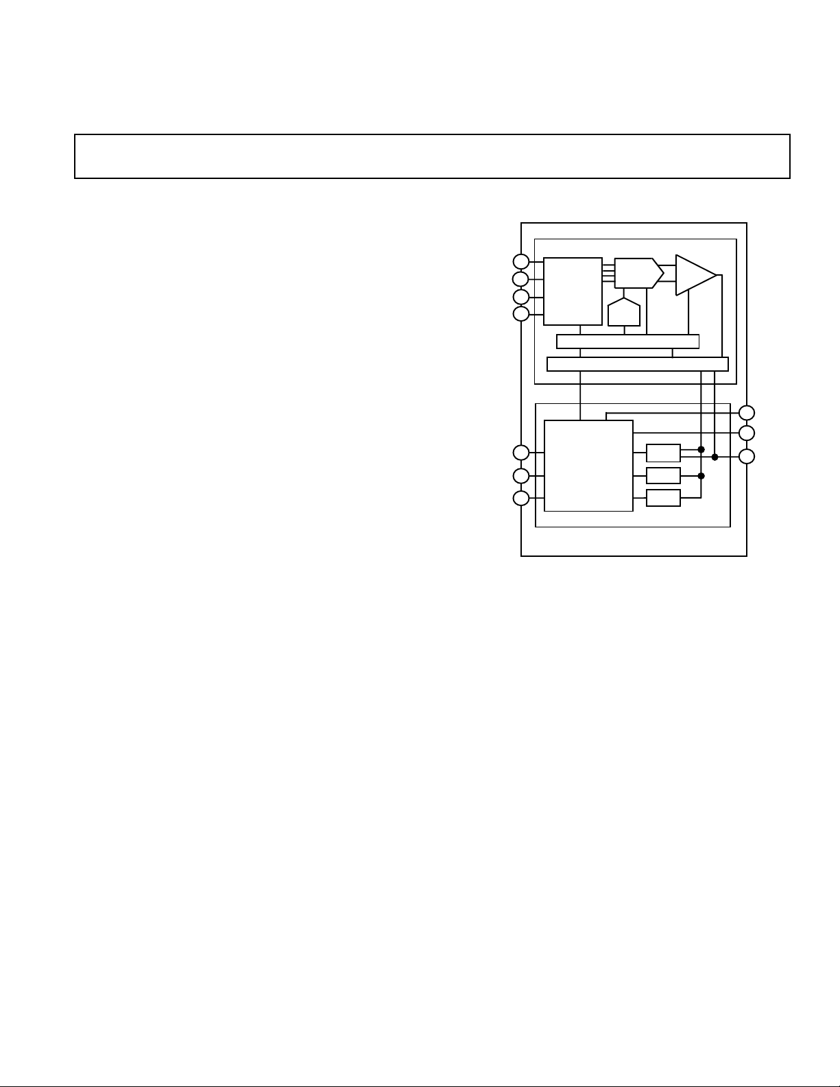
AGND
V
REF
COMP
A CHIP
V
IN
8
10
11
9
LEVEL TRANSLATORS
LOGIC TIMING
16-BIT
DAC
INPUT
BUFFERS
CAL
DAC
CLK
SAMPLE
D CLK
OUT
D CHIP
D
OUT
3
14
AD1876
2
16
1 RAM
ALU
SAR
AGND
SENSE
CAL
15 BUSY
MICROCODED
CONTROLLER
16-Bit 100 kSPS
a
FEATURES
Autocalibrating
0.002% THD
90 dB S/(N+D)
1 MHz Full Power Bandwidth
On-Chip Sample & Hold Function
23 Oversampling for Audio Applications
16-Pin DIP Package
Serial Twos Complement Output Format
Low Input Capacitance–typ 50 pF
AGND Sense for Improved Noise Immunity
PRODUCT DESCRIPTION
The AD1876 is a 16-bit serial output sampling A/D converter
which uses a switched capacitor/charge redistribution architecture
to achieve a 100 kSPS conversion rate (10 µs total conversion
time). Overall performance is optimized by digitally correcting
internal nonlinearities through on-chip autocalibration.
The circuitry of the AD1876 is partitioned onto two monolithic
chips, a digital control chip fabricated with Analog Devices’
DSP CMOS process and an analog ADC chip fabricated with
the BiMOS II process. Both chips are contained in a single
package.
The serial output interface requires an external clock and
sample command signal. The output data rate may be as high
as 2.08 MHz, and is controlled by the external clock. The twos
complement format of the output data is MSB first and is directly compatible with the NPC SM5805 digital decimation filter used in consumer audio products. The AD1876 is also
compatible with a variety of DSP processors.
The AD1876 is packaged in a space saving 16-pin plastic DIP
and operates from +5 V and ±12 V supplies; typical power consumption is 235 mW. The digital supply (V
the linear supplies (V
Separate analog and digital grounds are also provided.
and VCC) for reduced digital crosstalk.
EE
) is isolated from
DD
Sampling ADC
AD1876
FUNCTIONAL BLOCK DIAGRAM
REV. A
Information furnished by Analog Devices is believed to be accurate and
reliable. However, no responsibility is assumed by Analog Devices for its
use, nor for any infringements of patents or other rights of third parties
which may result from its use. No license is granted by implication or
otherwise under any patent or patent rights of Analog Devices.
One Technology Way, P.O. Box 9106, Norwood, MA 02062-9106, U.S.A.
Tel: 617/329-4700 Fax: 617/326-8703
Page 2

AD1876–SPECIFICA TIONS
(T
to T
MIN
, VCC = +12 V 6 5%, VEE = –12 V 6 5%, VDD = +5 V 6 10%)
MAX
1
AD1876J
Parameter Min Typ Max Units
TEMPERATURE RANGE 0 70 °C
TOTAL HARMONIC DISTORTION (THD)
2
–0.05 dB Input –95 –88 dB
0.002 0.004 %
–20 dB Input –78 dB
0.01 %
–60 dB Input –40 dB
1.0 %
D-RANGE, –60 dB, A-WEIGHTED 92 dB
SIGNAL-TO-NOISE AND DISTORTION (S/(N+D)) RATIO
3
–0.05 dB Input, A-Weighted 92 dB
–0.05 dB Input, 48 kHz Bandwidth 83 90 dB
–20 dB Input, A-Weighted 73 dB
–20 dB Input, 48 kHz Bandwidth 70 dB
–60 dB Input, A-Weighted 34 dB
–60 dB Input, 48 kHz Bandwidth 31 dB
PEAK SPURIOUS OR PEAK HARMONIC COMPONENT –99 –89 dB
INTERMODULATION DISTORTION (IMD)
4
2nd Order Products –102 dB
3rd Order Products –98 dB
FULL POWER BANDWIDTH 1 MHz
VOLTAGE REFERENCE INPUT RANGE5 (V
ANALOG INPUT
6
Input Range (VIN) ±V
)3510.0 V
REF
REF
V
Input Impedance *
Input Capacitance During Sample 50* pF
Aperture Delay 6ns
Aperture Jitter 100 ps
POWER SUPPLIES
Operating Current
I
CC
I
EE
I
DD
912mA
912mA
312mA
Power Consumption 235 350 mW
NOTES
1
V
= 5.00 V; conversion rate = 96 kSPS; fIN = 1.06 kHz; VIN = –0.05 dB unless otherwise noted. All measurements referred to a 0 dB (10 V p-p) input signal.
REF
Values are post calibration.
2
Includes first 19 harmonics.
3
Minimum value of S/(N+D) corresponds to 5.0 V reference; typical values of S/(N+D) correspond to 10.0 V reference.
4
fa = 1008 Hz; fb = 1055 Hz. See Definition of Specifications section and Figure 14.
5
See Applications section for recommended voltage reference circuit and Figure 11 for performance with other reference voltage values.
6
See Applications section for recommended input buffer circuit.
*For explanation of input characteristics, see “Analog Input” section.
Specifications subject to change without notice.
Specifications shown in boldface are tested on all devices at final electrical test at worst case temperature. Results from those tests are used to calculate outgoing
quality levels. All min and max specifications are guaranteed, although only those shown in boldface are tested.
ORDERING GUIDE
Temperature THD Package Package
Model Range dB Description Option*
AD1876JN 0°C to +70°C –95 Plastic 16-Pin DIP N-16
*N = Narrow Plastic DIP.
–2–
REV. A
Page 3
AD1876
WARNING!
ESD SENSITIVE DEVICE
(T
to T
DIGITAL SPECIFICATIONS
MIN
Parameter Test Conditions Min Typ Max Units
LOGIC INPUTS
V
IH
V
IL
I
IH
I
IL
C
IN
High Level Input Voltage 2.4 V
Low Level Input Voltage –0.3 0.8 V
High Level Input Current VIH = V
Low Level Input Current VIL = 0 V –10 +10 µA
Input Capacitance 10 pF
LOGIC OUTPUTS
V
OH
V
OL
Specifications subject to change without notice.
Specifications shown in boldface are tested on all devices at final electrical test at worst case temperature. Results from those tests are used to calculate outgoing qual-
ity levels. All min and max specifications are guaranteed, although only those shown in boldface are tested.
High Level Output Voltage IOH = 0.1 mA VDD – 1 V V
Low Level Output Voltage IOL = 1.6 mA 0.4 V
ABSOLUTE MAXIMUM RATINGS*
VCC to VEE . . . . . . . . . . . . . . . . . . . . . . . . . . –0.3 V to +26.4 V
V
to DGND . . . . . . . . . . . . . . . . . . . . . . . . . –0.3 V to +7 V
DD
V
to AGND . . . . . . . . . . . . . . . . . . . . . . . . –0.3 V to +18 V
CC
V
to AGND . . . . . . . . . . . . . . . . . . . . . . . . –18 V to +0.3 V
EE
AGND to DGND . . . . . . . . . . . . . . . . . . . . . . . . . . . . ±0.3 V
Digital Inputs to DGND . . . . . . . . . . . . . . . . . . . 0 V to 5.5 V
Analog Inputs, V
to AGND . . . . . . . . . . . (VCC + 0.3 V) to
REF
, VCC = +12 V 6 5%, VEE = –12 V 6 5%, VDD = +5 V 6 10%)
MAX
DD
I
= 0.5 mA 2.4 V
OH
–10 +10 µA
Soldering . . . . . . . . . . . . . . . . . . . . . . . . . . . . . +300°C, 10 sec
Storage Temperature . . . . . . . . . . . . . . . . . . –60°C to +100°C
*Stresses greater than those listed under “Absolute Maximum Ratings” may
cause permanent damage to the device. This is a stress rating only and
functional operation of the device at these or any other conditions above those
indicated in the operational section of this specification is not implied. Exposure
to absolute maximum rating conditions for extended periods may affect device
(V
– 0.3 V)
EE
reliability.
CAUTION
ESD (electrostatic discharge) sensitive device. Electrostatic charges as high as 4000 V readily
accumulate on the human body and test equipment and can discharge without detection.
Although the AD1876 features proprietary ESD protection circuitry, permanent damage may
occur on devices subjected to high energy electrostatic discharges. Therefore, proper ESD
precautions are recommended to avoid performance degradation or loss of functionality.
TIMING SPECIFICATIONS
Parameter Symbol Min Typ Max Units
Sampling Rate
Sampling Period
Acquisition Time (Included in t
Calibration Time t
CLK Period t
CAL to BUSY Delay t
CLK to BUSY Delay t
CLK to D
CLK HIGH t
CLK LOW t
D
OUT
SAMPLE LOW to 1st CLK Delay t
CAL HIGH Time t
CLK to D
SAMPLE LOW t
NOTES
1
See Figure 1 and Figure 2 and the Conversion Control and Autocalibration sections for detailed explanations of the above timing.
2
Depends upon external clock frequency; includes acquisition time and conversion time. The minimum sampling rate/maximum sampling period is specified to
account for droop of the internal sample/hold. Operation at slower rates than specified may degrade performance.
REV. A
1
(T
to T
MIN
MAX
2
2
)t
S
Hold Time t
OUT
CLK LOW t
CLK t
OUT
, VCC = +12 V 6 5%, VEE = –12 V 6 5%, VDD = +5 V 6 10%, V
fS = 1/t
S
tS = l/f
S
A
CT
C
CALB
CB
CD
CH
CL
DCL
SC
CALH
CDH
SL
1 100 kSPS
10 1000 µs
2 µs
480 ns
0ns
50 120 175 ns
10 ns
160 ns
50 ns
30 80 200 ns
50 ns
4t
150 200 275 ns
50 ns
–3–
= 5.00 V)
REF
5000 t
C
C
Page 4
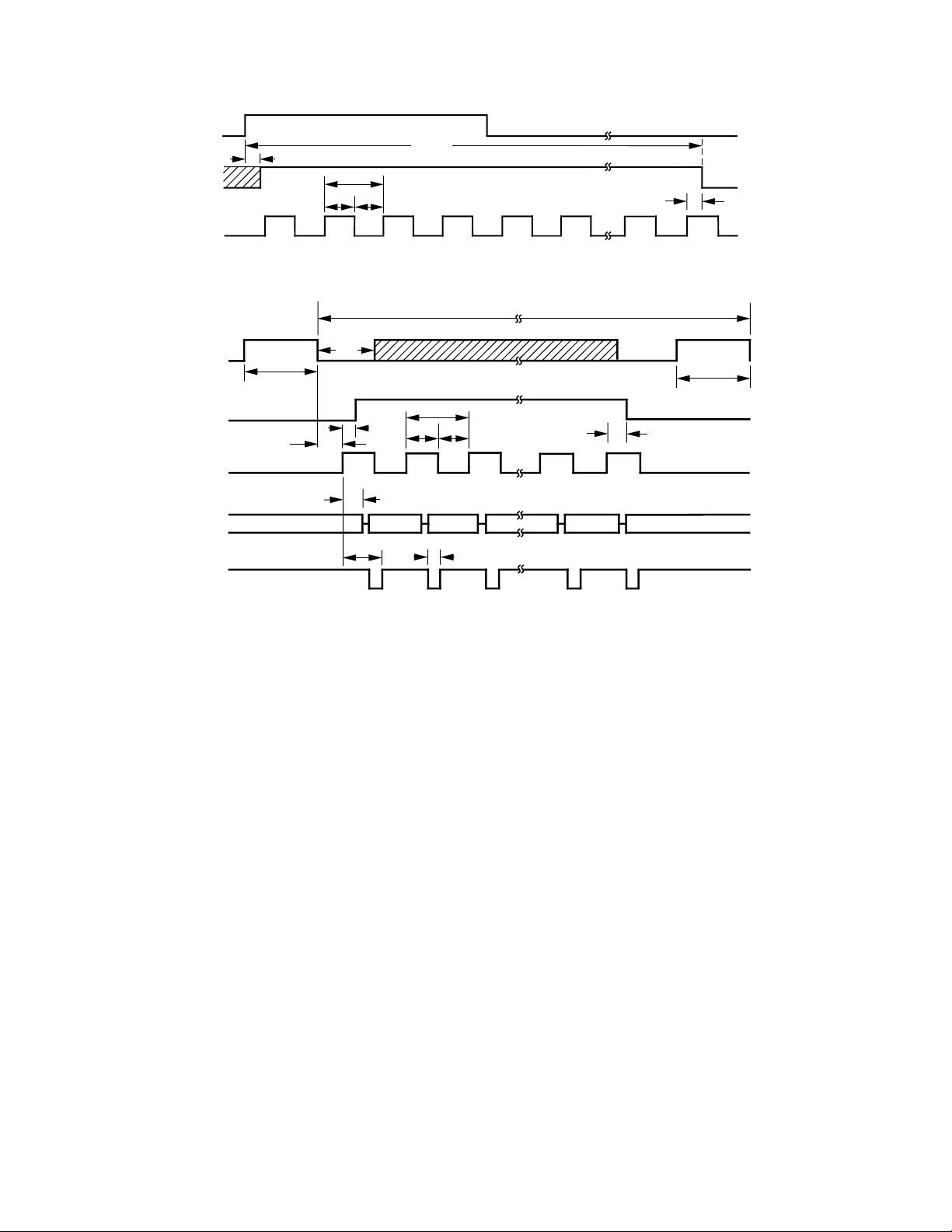
AD1876
CAL
BUSY
CLK
SAMPLE
BUSY
D
OUT
CLK
D
OUT
CLK
t
CALB
t
A
PREVIOUS LSB
t
CT
t
C
tCHt
CL
Figure 1. AD1876 Calibration Timing
tS (=1/fs)
t
SL
t
C
t
tCHt
1
t
CDH
CB
t
CD
X
t
SC
CL
2
MSB
t
3
DCL
t
CB
t
A
t
CB
16
17
LSB
Figure 2. Recommended AD1876 Conversion Timing
Definition of Specifications
NYQUIST FREQUENCY
An implication of the Nyquist sampling theorem, the “Nyquist
Frequency” of a converter is that input frequency which is onehalf the sampling frequency of the converter.
TOTAL HARMONIC DISTORTION
Total harmonic distortion (THD) is measured as the ratio of the
rms sum of the first nineteen harmonic components to the rms
value of a 1 kHz full-scale sine wave input signal and is expressed in percent (%) or decibels (dB). For input signals or
harmonics that are above the Nyquist frequency, the aliased
component is used.
SIGNAL-TO-NOISE PLUS DISTORTION RATIO
Signal-to-noise plus distortion (S/N+D) is defined to be the ratio of the rms value of the measured input signal to the rms sum
of all other spectral components below the Nyquist frequency,
including harmonics but excluding dc.
D-RANGE DISTORTION
D-range distortion is the ratio of the distortion plus noise to the
signal at a signal amplitude of –60 dB. In this case, an A-weight
filter is used. The value specified for D-range performance is the
ratio measured plus 60 dB.
BANDWIDTH
The full power bandwidth is that input frequency at which the
amplitude of the reconstructed fundamental is reduced by 3 dB
for a full-scale input.
INTERMODULATION DISTORTION (IMD)
With inputs consisting of sine waves at two frequencies, fa and
f
, any device with nonlinearities will create distortion products,
b
of order (m+n), at sum and difference frequencies of mf
± nfb,
a
where m, n = 0, l, 2, 3. . . . Intermodulation terms are those for
which m or n is not equal to zero. For example, the second order terms are (f
(2f
+ fb), (2fa – fb), (fa + 2fb) and (fa – 2fb). The IMD products
a
+ fb) and (fa – fb), and the third order terms are
a
are expressed as the decibel ratio of the rms sum of the measured input signals to the rms sum of the distortion terms. The
two signals applied to the converter are of equal amplitude, and
the peak value of their sum is –0.05 dB from full scale. The
IMD products are normalized to a 0 dB input signal.
APERTURE DELAY
Aperture delay is the time required after SAMPLE is taken
LOW for the internal sample-hold of the AD1876 to open, thus
holding the value of V
.
IN
APERTURE JITTER
Aperture jitter is the variation in the aperture delay from sample
to sample.
–4–
REV. A
Page 5

Pin
AGND
V
REF
COMP
A CHIP
V
IN
8
10
11
9
LEVEL TRANSLATORS
LOGIC TIMING
16-BIT
DAC
INPUT
BUFFERS
CAL
DAC
CLK
SAMPLE
D CLK
OUT
D CHIP
D
OUT
3
14
AD1876
2
16
1 RAM
ALU
SAR
AGND
SENSE
CAL
15 BUSY
MICROCODED
CONTROLLER
No. Name Type Description
AD1876
PIN DESCRIPTION
1 SAMPLE DI V
Acquisition Control Pin. During conversion, SAMPLE controls the state of the internal
IN
Sample-Hold Amplifier and initiates conversion (see “Conversion Control” paragraph). During calibration, SAMPLE is active HIGH, forcing D
during calibration, D
will output diagnostic information (See “Autocalibration” paragraph.)
OUT
(Pin 3) LOW. If SAMPLE is LOW
OUT
2 CLK DI Master Clock Input. The AD1876 requires 17 clock pulses to execute a conversion. CLK is
3D
OUT
also used to derive D
DO Serial Output Data, Twos Complement format.
CLK (Pin 14). During calibration, 5000 clock pulses are applied.
OUT
4 DGND P Digital Ground.
5V
CC
P +12 V Analog Supply Voltage.
6 N/C – No Connection.
7 N/C – No Connection.
8 AGND P/AI Analog Ground.
9 AGND SENSE AI Analog Ground Sense.
10 V
11 V
12 V
13 V
14 D
IN
REF
EE
DD
CLK DO The rising edge of D
OUT
AI Analog Input Voltage, referred the AGND SENSE.
AI External Voltage Reference Input, referred to AGND.
P –12 V Analog Supply Voltage.
P +5 V Logic Supply Voltage.
CLK may be used to latch D
OUT
OUT
(Pin 3). D
CLK is derived from
OUT
CLK.
15 BUSY DO Status Line for Converter. Active HIGH, indicating a conversion or calibration in progress.
16 CAL DI Calibration Control Pin (asynchronous).
Type: AI = Analog Input.
DI = Digital Input.
DO = Digital Output.
P = Power.
REV. A
1
SAMPLE
2
CLK
3
D
OUT
4
DGND
5
V
CC
6
NC
7
NC
8
AGND
NC = NO CONNECT
Package Pinout
AD1876
TOP VIEW
(Not to Scale)
16
CAL
15
BUSY
14
D
OUT
13
V
DD
12
V
EE
11
V
REF
V
10
IN
AGND SENSE
9
CLK
Functional Block Diagram
–5–
Page 6

AD1876
FUNCTIONAL DESCRIPTION
The AD1876 is a 16-bit analog-to-digital converter including a
sample/hold input circuit, successive approximation register,
ground sensing circuitry, serial output port and a microcontroller based autocalibration circuit. These functions are segmented onto two monolithic chips, an analog signal processor
and a digital controller. Both chips are contained within the
AD1876 package.
The AD1876 employs a successive-approximation technique to
determine the value of the analog input voltage. However, instead of the traditional laser-trimmed resistor-ladder approach,
the AD1876 uses a capacitor-array, charge-redistribution technique. An array of binary-weighted capacitors subdivides the
input value to perform the actual analog to digital conversion.
This capacitor array also serves a sample/hold function without
the need for additional external circuitry.
The autocalibration circuit within the AD1876 employs a
microcontroller and calibration DAC to measure and compensate capacitor mismatch errors. As each error is determined, its
value is stored in on-chip memory (RAM). Subsequent conversions use these RAM values to improve conversion accuracy.
The autocalibration routine may be invoked at any time. Autocalibration insures high performance while eliminating the need
for any user adjustments, and is described in detail below.
The microcontroller controls all of the various functions within
the AD1876. These include the actual successive approximation
routine, the autocalibration routine, the sample/hold operation,
and the serial data transmission.
AUTOCALIBRATION
The AD1876 achieves rated performance without the need for
user trims or adjustments. This is accomplished through the use
of on-chip autocalibration.
In the autocalibration sequence, sample/hold offset is nulled by
internally connecting the input circuit to the ground sense circuit. The resulting offset voltage is measured and stored in
RAM for later use. Next, the capacitor representing the most
significant bit (MSB) is charged to the reference voltage. This
charge is then inverted and shared between the MSB capacitor
and one of equal size composed of all the least significant bits.
The difference in the summation of the charges in each of the
equally sized capacitors represents the amount of capacitor mismatch. A calibration D/A converter (DAC) adds an appropriate
value of error correction voltage to cancel the mismatch. This
correction factor is also stored in RAM. This process is repeated
for each of the capacitors representing the remaining bits. The
accumulated values in RAM are then used during subsequent
conversions to adjust conversion results.
As shown in Figure 1, when CAL is taken HIGH the AD1876
internal circuitry is reset, the BUSY pin is driven HIGH and the
part prepares for calibration. This is a ‘hard’ reset and will interrupt any conversion or calibration currently in progress. In order
to guarantee that all internal undefined states are cleared, the
CAL pin should he held HIGH for at least 4 CLK cycles. Actual calibration begins when the CAL pin is taken LOW and
completes in less than 5000 clock cycles or about 2.5 msec with
a continuous 500 nsec clock.
During calibration the SAMPLE pin adopts an alternative function. If it is held LOW, D
provides diagnostic test informa-
OUT
tion (not intended to be used by the customer). If SAMPLE is
held HIGH, D
will be forced LOW. In either case, D
OUT
OUT
CLK will continue pulsing. Since the SAMPLE pin has no control over the actual calibration process, normal conversion timing may also be used for calibration. In this case, however, the
D
pin will output test information during those periods that
OUT
SAMPLE is LOW. BUSY going LOW will always indicate the
end of calibration.
A calibration sequence should be followed by one “dummy”
conversion to clear the internal circuitry of the AD1876 in order
to guarantee subsequent conversion accuracy.
In most applications, it is sufficient to calibrate the AD1876
only upon power-up, in which case care should be taken that the
power supplies and voltage reference have stabilized first.
CONVERSION CONTROL
The AD1876 is controlled by two signals: SAMPLE and CLK,
as shown in Figure 2. It is assumed that the part has been calibrated and the digital I/O pins have the levels shown at the start
of the timing diagram.
A conversion consists of an input acquisition followed by 17
clock pulses which are required to run the 16-bit internal successive approximation routine. The analog input is acquired by
taking the SAMPLE line HIGH for a minimum acquisition time
of t
. The actual sample taken is the voltage present on VIN at
A
the instant the SAMPLE pin is brought LOW. Care should be
taken to ensure that this negative edge is well defined and jitter
free to reduce the uncertainty (noise) in ac signal acquisition.
On that edge the AD1876 commits itself to the initiated conversion—the input at V
is disconnected from the internal capaci-
IN
tor array and the SAMPLE input will be ignored until the
conversion is completed (i.e., BUSY goes LOW). After a delay
of at least t
(SAMPLE to CLK setup) the 17 CLK cycles are
SC
applied. BUSY is asserted after the first positive edge on CLK
and reset after the 17th. Both the D
and the D
OUT
CLK out-
OUT
puts are generated in response to the rising edges of valid CLK
pulses. As indicated in the timing diagram, the 2s complement
output data is presented MSB first. This data may be captured
with the rising edge of D
provided t
CH
≥ t
. The AD1876 will ignore CLK after BUSY
CDH
has gone LOW and not change D
CLK or the falling edge of CLK
OUT
OUT
or D
CLK until a new
OUT
sample is acquired. SAMPLE will no longer be ignored after
BUSY goes LOW, and so an acquisition may be initiated even
during the HIGH time of the 17th CLK pulse for maximum
throughput rate while enabling full settling of the sample/hold
circuitry. Note that if SAMPLE is already HIGH when BUSY
goes LOW, then an acquisition is immediately initiated and t
A
starts from that time.
During signal acquisition and conversion, care should be taken
with the logic inputs to avoid digital feedthrough noise. It is not
recommended that CLK be running during V
sampling. If a
IN
continuous CLK is used, then the user must avoid CLK edges
at the instant of disconnecting V
SAMPLE (see the t
CLK (t
) should be at least 100 ns to avoid the negative edge
CL
specifications). The LOW level time of
SC
, i.e., the falling edge of
IN
transition disturbing the internal comparator’s settling (whose
decision is latched on the positive edge of each valid CLK). For
the same reason, it is also not recommended that the SAMPLE
pin change state during conversion (i.e., until after BUSY returns LOW).
–6–
REV. A
Page 7

AD1876
Internal dc error terms such as comparator voltage offset are
sampled, stored on internal capacitors and used to correct for
their corresponding errors when needed. Because these voltages
are stored on capacitors, they are subject to leakage decay and
so require refreshing. For this reason the part is required to be
run continuously—i.e., there is a minimum t
the part has been idle for too long (i.e., t
specification. If
S
has expired) then a
S
dummy conversion cycle is required to refresh these correction
voltages.
BUSY is HIGH during a conversion and goes LOW when the
conversion is completed. The twos complement output data is
presented MSB first, with MSB data valid on the rising edge of
the second D
edges of subsequent D
CLK pulse. Subsequent data is valid on rising
OUT
CLK pulses. Table I illustrates the
OUT
AD1876 output coding.
Table I. Serial Output Coding Format (Twos Complement)
V
IN
Output Code
–Full Scale 100 . . . 00
–Full Scale + 1 LSB 100 . . . 01
Midscale – 1 LSB 111 . . . 11
Midscale 000 . . . 00
Midscale + 1 LSB 000 . . . 01
Full Scale – 1 LSB 011 . . . 10
Full Scale 011 . . . 11
A simple method for generating the required signals for the
AD1876 is to connect one or more AD1876s to an NPC
SM5805 digital filter. This device supplies all signals required to
operate the AD1876 at a 96 kHz sample rate, which is 2 × F
for
S
audio applications. This is more fully discussed in the applications
section of this data sheet, accompanied by Figures 9 and 10.
APPLICATIONS
POWER SUPPLIES AND DECOUPLING
The AD1876 has three power supply input pins. VEE and V
CC
provide the supply voltages to operate the analog portions of the
AD1876 including the ADC and SHA. V
provides the supply
DD
voltage which operates the digital portions of the AD1876 including the serial output port and the autocalibration controller.
Decoupling capacitors should he used on all power supply pins.
These capacitors should be placed as close as possible to the
package pins as well as the ground connections. The logic supply (V
with a 0.1 µF ceramic capacitor, and the analog supplies (V
) should be decoupled to digital common (DGND)
DD
EE
and VCC) should be decoupled to analog common (AGND)
with 4.7 µF and 0.1 µF tantalum capacitors in parallel, repre-
sented by C1. An effort should be made to minimize the trace
length between the capacitor leads and the respective converter
power supply and common pins. The recommended decoupling
scheme is illustrated in Figure 3.
As with most high performance linear circuits, changes in the
power supplies can produce undesired changes in the performance of the circuit. Analog Devices recommends that well
regulated power supplies with less than 1% ripple be incorporated into the design of any system using these devices.
BOARD LAYOUT
Designing with high resolution data converters requires careful
attention to board layout. Trace impedance is a significant issue.
A 1.22 mA current through a 0.5 Ω trace will develop a voltage
drop of 0.6 mV, which is 4 LSBs at the 16 bit level for a 10 V
full-scale span. In addition to ground drops, inductive and capacitive coupling need to be considered, especially when high
accuracy analog signals share the same board with digital signals. Finally, power supplies need to be decoupled in order to
filter ac noise.
Analog and digital signals should not share a common return
path. Each signal should have an appropriate analog or digital
return routed close to it. Using this approach, signal loops enclose a small area, minimizing the inductive coupling of noise.
Wide PC tracks, large gauge wire, and ground planes are highly
recommended to provide low impedance signal paths. Separate
analog and digital ground planes are also desirable, with a single
interconnection point to minimize ground loops. Analog signals
should be routed as far as possible from digital signals and
should cross them, if at all, only at right angles. A solid analog
ground plane around the AD1876 will isolate large switching
ground currents. For these reasons, the use of wire wrap circuit
construction is not recommended; careful printed circuit construction is preferred.
13
5V
0.1µF
V
DD
SYSTEM
DIGITAL
COMMON
AD1876
4
AGNDDGND
8
SYSTEM
ANALOG
COMMON
AGND SENSE
VCCV
C1
12V –12V
C1
Figure 3. Grounding and Decoupling the AD1876
REV. A
GROUNDING
V
11
REF
V
10
IN
9
The AD1876 has three grounding pins, designated ANALOG
GROUND (AGND), DIGITAL GROUND (DGND) and
ANALOG GROUND SENSE (AGND SENSE). The analog
ground pin is the “high quality” ground reference point for the
device. The analog ground pin should be connected to the analog common point in the system.
EE
12
5
AGND SENSE is intended to be connected to the input signal
ground reference point. This allows for slight differences in level
between the analog ground point in the system and the input
signal ground point. However, no more than 100 mV is recommended between the analog ground pin and the analog ground
sense pin for specified performance.
The digital ground pin is the reference point for all of the digital
signals that operate the AD1876. This pin should be connected
to the digital common point in the system. As illustrated in Figure 3, the analog and digital grounds should be connected together at one point in the system.
–7–
Page 8

AD1876
VOLTAGE REFERENCE
The AD1876 requires the use of an external voltage reference.
The input voltage range is determined by the value of the reference voltage; in general, a reference voltage of n volts produces
an input range of ±n volts. Signal-to-noise performance is increased proportionately with input signal range. The AD1876 is
specified with a 5.0 V reference and an analog input of ±5 V. In
the presence of a fixed amount of system noise, increasing the
LSB size (which results from increasing the reference voltage)
will increase the effective S/(N+D) performance for input values
below the point where input distortion occurs. Figure 11 illustrates S/(N+D) as a function of input amplitude and reference
voltage.
During a conversion, the switched capacitor array of the
AD1876 presents a dynamically changing current load at the
voltage reference as the successive-approximation algorithm
cycles through various choices of capacitor weighting. The output impedance of the reference circuitry must be low so that the
output voltage will remain sufficiently constant as the current
drive changes. In most applications, this requires that the output
of the voltage reference be buffered by an amplifier with low impedance at relatively high frequencies. A (10 µF or larger) ca-
pacitor connected between V
and AGND will reduce the
REF
demands on the reference by decreasing the magnitude of high
frequency components.
The following two sections represent typical design approaches.
VOLTAGE REFERENCE—AUDIO APPLICATIONS
Audio applications require optimal ac performance over a relatively narrow temperature range, with low cost being important.
Figure 4 shows one such approach towards attaining these goals.
A voltage reference, consisting of a Zener diode, capacitor, resistor and op amp with typical component values, is shown. This
simple circuit has the advantage of low cost, but the reference
voltage value is sensitive to changes in the +12 V supply. Additionally, changes in the Zener value due to temperature variations will also be reflected in the reference voltage. R
OPTION
may
be required for other component selections if the Zener requires
more current than the op amp can supply.
+
R
OPTION
1kΩ
+70°C range, the AD586L grade exhibits less than a 2.25 mV
output change from its initial value at +25°C. A noise-reduction
capacitor, C
, reduces the broadband noise of the AD586 out-
N
put, thereby optimizing the overall performance of the AD1876.
+12V
2
V
11
REF
+
AD1876
AGND
8
C
1µF
8
N
AD586
4
6
47µF
AGND
Figure 5.
For higher performance needs, the AD588 reference provides
improved drift, low noise, and excellent initial accuracy. The
AD588 uses a proprietary ion-implanted buried Zener diode in
conjunction with laser-trimmed thin-film resistors for low offset
and gain. The AD588 output is accurate to 0.65 mV from its
value at +25°C over the 0°C to +70°C range. The circuit shown
in Figure 6 includes a noise-reduction network on Pins 4, 6 and
7. The 1 µF capacitors form low-pass filters with the internal re-
sistance of the AD588 and external 3.9 kΩ resistor. This reduces the wide-band (to 1 MHz) noise of the AD588, providing
optimum performance of the AD1876.
+12V
–12V
1µF
NOISE
REDUCTION
0.1µF
0.1µF
16
3.9kΩ
2
AD588
581312
NC NC
NC
1µF
3467
V
1
9
10
11
47µF
AGND
11
8
AGND
AD1876
REF
V
REF
AD711
AD589
0.1µF
11
3kΩ
1kΩ
AD1876
Figure 4. Low Cost Voltage Reference Circuit
VOLTAGE REFERENCE—PRECISION MEASUREMENT
APPLICATIONS
In applications other than audio, parameters such as low drift
over temperature and static accuracy are important. Figure 5
shows a voltage reference circuit featuring the 5 V AD586. The
AD586 is a low cost reference which utilizes a buried Zener architecture to provide low noise and drift. Over the 0°C to
–8–
Figure 6.
ANALOG INPUT
As previously discussed, the analog input voltage range for the
AD1876 is ±V
mode rejection, the V
ground. V
(AGND), and V
. For purposes of ground drop and common-
REF
is referred to the local analog system ground
REF
and V
IN
is referred to the analog ground sense pin
IN
inputs each have their own
REF
(AGND SENSE) which allows a remote ground sense for the
input signal. If AGND SENSE is not used, it should be connected to the AGND pin at the package. The AGND SENSE
pin is intended to be tied to potentials within 100 mV of AGND
to maintain specified performance.
The AD1876 analog inputs (V
, V
IN
and AGND SENSE)
REF
exhibit dynamic characteristics. When a conversion cycle begins,
each analog input is connected to an internal, discharged 50 pF
capacitor which then charges to the voltage present at the
REV. A
Page 9

AD1876
corresponding pin. The capacitor is disconnected when SAMPLE
is taken LOW and the stored charge is used in the subsequent
A/D conversion. In order to limit the demands placed on the
external source by this high initial charging current, an internal
buffer amplifier is employed between the input and this capacitance for a few hundred nanoseconds. During this time the
input pin exhibits typically 20 kΩ input resistance, 10 pF input
capacitance and ±40 µA bias current. Next, the input is switched
directly to the now precharged capacitor and allowed to fully
settle, after which SAMPLE is taken LOW. During this time
the input sees only a 50 pF capacitor. Once the sample is taken,
the input is internally floated so that the external input source
sees a very high input resistance and a parasitic input capacitance of typically only 2 pF. As a result, the only dominant input
characteristic which must be considered is the high current steps
which occur when the internal buffers are switched in and out.
In most cases, it is desirable to use external op amps to drive the
AD1876. For ac applications where low cost and low distortion
are desired, the AD711 may be used as shown in Figure 7. Another option is the 5532/5534 series. Care should always be
taken with op amp selection—many available op amps do not
meet the necessary low distortion requirements with even moderate loading conditions.
1kΩ
+12V
0.1µF
V
IN
1kΩ
499Ω
2
3
AD711
–12V
7
6
4
0.1µF
10
V
IN
AD1876
AGND
8
9
AGND SENSE
Figure 7.
TESTING THE AD1876
Analog Devices employs a high performance mixed signal VLSI
tester to verify the electrical performance of every AD1876. The
test system consists of two main sections, an input signal generator and a digital data and control section.
The stimulus section is responsible for providing a high purity,
noise-free, band limited tone to the input of the device. This input frequency is 1.06 kHz. The test tone is passed through a
bandpass filter to remove distortion products and then buffered
by a high performance op amp. An external 5.000 V reference
voltage is also supplied by this section.
The control section of the test equipment provides an external
clock and the control signals for calibration, conversion and data
transmission. This section of the tester also contains the processing unit that calculates the actual performance of the device
under test.
The test procedure consists of the following steps. First, the
device is calibrated by its on-board controller. Next, the device
under test digitizes the input waveform. This conversion is
performed at a 96 kSPS rate and transmits the resulting serial
data to the tester. The tester performs an FFT on the test data
and determines the actual performance of the device.
AC PERFORMANCE
Using the aforementioned test methodology, ac performance
of the AD1876 is measured. AC parameters, which include
S/(N+D), THD, etc., reflect the AD1876’s effect on the spectral content of the analog input signal. Figures 11 through 15
provide information on the AD1876’s ac performance under a
variety of conditions.
As a general rule, averaging the results from several conversions
reduces the effects of noise and, therefore, improves such parameters as S/(N+D) and THD. AD1876 performance is optimized by operating the device at its maximum sample rate of
100 kSPS and digitally filtering the resulting bit stream to the
desired signal bandwidth. This succeeds in distributing noise
over a wider frequency range, thus reducing the noise density in
the frequency band of interest. This subject is discussed in the
following section.
OVERSAMPLING AND NOISE FILTERING
The Nyquist rate for a converter is defined as one-half its sampling rate. This is established by the Nyquist theorem, which
requires that a signal be sampled at a rate corresponding to at
least twice its widest bandwidth of interest in order to preserve
the information content. Oversampling is a conversion technique in which the sampling frequency is an integral (2 or more)
multiple of twice the frequency bandwidth of interest. In audio
applications, the AD1876 can operate at a 2× oversampling rate.
In quantized systems, the information content of the analog input is represented in the frequency spectrum from dc to the
Nyquist rate of the converter. Within this same spectrum are
higher frequency aliased noise components. Antialias, or lowpass, filters are used at the input to the ADC to remove the portion of these noise components attributed to high frequency
analog input noise. However, wideband noise contributed by the
AD1876 will not be reduced by the antialias filter. The AD1876
contributed noise is evenly distributed from dc to the Nyquist
rate, and this fact can be used to minimize its overall effect.
The AD1876 contributed noise effects can be reduced by
oversampling—sampling at a rate higher than defined by the
Nyquist theorem. This spreads the noise energy over a distribution of frequencies wider than the frequency band of interest,
and by judicious selection of a digital filter, noise frequencies
outside the bandwidth of interest may be eliminated. The process of quantization inherently produces noise, known as quantization noise. The magnitude of this noise is a function of the
resolution of the converter, and manifests itself as a limit to the
theoretical signal-to-noise ratio achievable. This limit is described by S/(N+D) = (6.02 n + 1.76 + 10 log F
where n is the resolution of the converter in bits, F
pling frequency, and F
is the signal bandwidth of interest. For
a
/2 Fa) dB,
S
is the sam-
S
audio bandwidth applications, the AD1876 is capable of operating at a 2× oversample rate (96 kSPS), which typically produces
an improvement in S/(N+D) of 3 dB compared with operating
at the Nyquist conversion rate of 48 kSPS. Oversampling has
another advantage as well; the demands on the antialias filter are
REV. A
–9–
Page 10

AD1876
lessened. In summary, system performance is optimized by running the AD1876 at or near its maximum sampling rate of
100 kHz and digitally filtering the resulting spectrum to eliminate undesired frequencies.
DSP INTERFACE
Figure 8 illustrates the use of the Analog Devices ADSP-2101
digital signal processor with the AD1876. The ADSP-2101 FO
(flag out) pin of serial port 1 (SPORT 1) is connected to the
SAMPLE line and is used to control acquisition of data. The
ADSP-2101 timer is used to provide precise timing of the FO
pin.
ADSP-2101
SERIAL
PORT Ø
FO
SCLK0
DR0
RFS0
DT0
TFS0
AD1876
SAMPLE
CLK
D
OUT
BUSY
Figure 8. ADSP-2101 Interface
The SCLK pin of the ADSP-2101 SPORT0 provides the CLK
input for the AD1876. The clock should be programmed to be
approximately 2 MHz to comply with AD1876 specifications.
To minimize digital feedthrough, the clock should be disabled
(by setting Bit 14 in SPORT0 control register to 0) during data
acquisition. Since the clock floats when disabled, a pull-down
resistor of 12 k–15 kΩ should be connected to SCLK to ensure
it will be LOW at the falling edge of SAMPLE. To maximize
the conversion rate, the serial clock should be enabled immediately after SAMPLE is brought LOW (hold mode).
The AD1876 BUSY signal is connected to RF0 to notify
SPORT0 when a new data word is coming. SPORT0 should be
configured in normal, external, noninverting framing mode and
LEFT
CHANNEL
INPUT
RIGHT
CHANNEL
INPUT
AD1876*
V
D
10
CLK SAMPLE
CLK SAMPLE
V
10
*ADDITIONAL PINS OMITTED FOR CLARITY
IN
OUT
2
2
D
OUT
IN
AD1876*
3
1
1
3
16
SH
18
BBC
IBLK
8
DINL
DINR ISLB IBPOL
Figure 9. AD1876 and SM5805 Digital Filter
can be programmed to generate an interrupt after the last data
bit is received. To maximize the conversion rate, SAMPLE
should be brought HIGH immediately after the last data bit is
received.
SIGNAL PROCESSING
An audio spectrum analyzer can be produced by combining an
AD1876 and an ADSP-2101 signal processing microcomputer.
This system can analyze signals from dc to 50 kHz depending
on the sample rate. This is ideal for applications such as audio
analysis, but could also be applied to vibration analysis as well.
AUDIO DELAY LINE
A high performance, 16-bit stereo delay line can be constructed
from two AD1876 audio ADCs, a signal processing microcomputer and two AD1856 audio DACs. Depending on the length
of the internal buffer which produces the delay, a variable delay
is possible. Other applications are also possible with only a
change in software. For example, a reverb or echo effect could
be generated as well.
AD1876 AND SM5805 DIGITAL FILTER @ 2 F
S
A simple method for generating the required signals for the
AD1876 is to connect one or more AD1876s to an NPC
SM5805 digital filter. This device supplies all signals required to
operate the AD1876 at a 96 kHz sample rate, which is 2 × F
S
for
audio applications.
To minimize group delay distortion, the input to the AD1876 is
filtered only by a low order analog filter. The AD1876 samples
the output of the filter at 2 F
(96 kHz). To prevent aliasing, the
S
SM5805 filters the data with a sharp, linear phase filter rolling
off at 0.5 F
. The resulting data is decimated to a sample rate of
S
48 kSPS.
Interfacing the two chips is straightforward, as shown in Figure
9. The start signal for the AD1876 (for 96 kSPS operation) is
provided by the S/H pin of the SM5805, and CLK is derived
from the BCC pin. Figure 10 illustrates the corresponding timing diagram.
1F (48kHz)
S
DOL
DOR
OFB
CLOCK
25
24
DECIMATED
DATA, LEFT
DECIMATED
DATA, RIGHT
4
IPARA
SM5805*
7
5
LEFT OPEN OR TIED
612
LRCK
U/O
10 11 15
TO +5V
OUTPUT
BBC
OUTPUT
DINL
DINR
1/f (f = 48kHz)
ss
SH
1
MSB
234567
MSB
234567
91011
8
91011
8
Lm
12 13
Rm
12 13
17
14
LSB
15
14
LSB
15
MSB
234567
MSB
234567
Lm + 1
Rm + 1
89
91011
8
10 11
12 13
12 13 14
14
15
LSB
15
LSB
Figure 10. SM5805 Timing Diagram
–10–
REV. A
Page 11

90
90
80
70
60
50
40
30
20
0 100 1k 10k 100k 1M
INPUT FREQUENCY – Hz
S/(N+D) – dB
–0dB INPUT
–20dB INPUT
–60dB INPUT
80
70
V
= 10V
60
50
40
S/(N+D) – dB
30
20
10
0
–80 –70 –60 –50 –40 –30 –20 –10 0
INPUT AMPLITUDE, REFERRED TO FULL-SCALE – dB
Figure 11. S/(N+D) vs. V
REF
V
= 5V
REF
V
= 7V
REF
vs. Input Amplitude
REF
T ypical Dynamic Performance–AD1876
Figure 12. S/(N+D) vs. Input Frequency and Amplitude
Figure 13. 4096 Point FFT at 96 kSPS, fIN = 1.06 kHz
90
80
70
60
50
S/(N+D) –dB
40
30
20
0
100 1k 10k 100k
RIPPLE FREQUENCY – Hz
Figure 15. Power Supply Rejection (fIN = 1.06 kHz,
= 96 kSPS, V
f
SAMPLE
Figure 14. IMD Plot for fIN = 1008 Hz (fa), 1055 Hz (fb) at
96 kSPS
+5V
+12V
–12V
1M
= 0.3 V p-p)
RIPPLE
REV. A
–11–
Page 12

AD1876
OUTLINE DIMENSIONS
Dimensions shown in inches and (mm).
Plastic DIP (N) Package
C1482–10–1/91
–12–
PRINTED IN U.S.A.
REV. A
 Loading...